Tailoring of optical properties of LiNbO 3 by ion implantation
|
|
|
- Angel Gaines
- 5 years ago
- Views:
Transcription

1 SMR/ "Workshop on Ion Beam Studies of Nanomaterials: Synthesis, Modification and Characterization" 26 June - 1 July 2006 Tailoring of Optical Properties of LiNbO3 by ion implantation Cinzia SADA Department of Physics University of Padova Padova, Italy
2 Tailoring of optical properties of LiNbO 3 by ion implantation Dr Cinzia Sada Physics Department,, University of Padova G.G. Bentini,, M. Bianconi, M. Chiarini IMM-CNR di Bologna N. Argiolas,, M. Bazzan,, P. Mazzoldi Physics Department,, University of Padova
3 Outline The material Optical properties Linear (LO) and nonlinear (NLO) optical response Exploitation of ion implantation for nanoclusters formation Exploitation of ion implantation for waveguides formation Applications: optical modulator for gas tracing Exploitation of ion implantation in photonics Photonic structures Realisation and characteristics Applications


4 The material C axis <001> Nb P s Lithium Niobate (LiNbO 3 ) O Li Nb Ferroelectric with a spontaneous polarization P s =0.71 C/m 2 parallel to the c- axis Due to its large Electro-Optic and Acousto-Optic coefficients, LiNbO 3 is used for optical applications: Li 1.Optical modulators 2.Pockel Cells switches, 3.Integrated waveguides 4.Second harmonic generation
5 Optical properties Linear optical properties Ordinary refractive index n o Extraordinary refractive n e (E c axis) (E // c axis) Negative birifrangence (at 633n) Transmission: 80% in the range 350nm-4000nm n e = n o = Nonlinear optical properties χ (2) =2d d=non linear optical coefficient d 31 (pm/v) d 33 (pm/v) d 22 (pm/v) LiNbO
6 Ion Implantation on LiNbO 3 LiNbO 3 LO properties NLO properties Induced NLO properties Optical waveguides Modification of the local composition and structure to confine the light Metal nanocluster in LiNbO 3 Application in nanotech Application in integrated optics
7 Applications of ion implantation on LiNbO 3 Local doping with passive elements (metals, H,He,..) Input Signal λ X:LiNbO 3 Output Signal λ Optical modulation Ti:LiNbO 3 O:LiNbO 3 H:LiNbO 3 Optical recording Fe:LiNbO 3 Cu:LiNbO 3 Local doping with active elements (rare earths ) Input Signal λ Amplification and lasing Output Signal λ Er:LiNbO 3 Er:glass/SiO 2

8 Applications of ion implantation on LiNbO 3 Native nonlinear properties Signal λ PPLN LiNbO 3 Second Harmonic Laser at λ/2 Blue-green wavelenth for Optical recording Induced nonlinear properpies ON configuration Off configuration Input Optical Switch Output Input Optical Switch Output
9 Induced nonlinear properties Ion implantation of metals in LiNbO 3 for realisation of metal nanoparticles Works reported in literature: implantation of Au, Ag, Cu in the KeV region Best results obtained on Cu:LiNbO 3
10 Induced nonlinear optical properties Cu- implanted at E=60KeV I=10-50 µa/cm 2

11 Induced nonlinear optical properties Cu- implanted at: E=60KeV I=10-50 µa/cm 2 Non spherical nanocluster D=10nm Sub-picosecond nonlinear response
12 Linear optical properties Ion implantation of: heavy elements (Si 30KeV), medium light (C,O,N 3-5MeV) light elements (H, He 0.5-1MeV) to modify locally the refractive index of the medium and guarantee the light confinement Waveguides for integrated optics
13 Linear optical properties: waveguide Light confinement in optical waveguides n waveguide -n substrate >0 Total internal reflection n atmosphere θ 2 θ 3 θ 2 n waveguide n substrate
14 Integrated optics: optical waveguide How to prepare an optical waveguide Standard approach Introduction of suitable dopant Alternative approach Modification of the surrounding Methods: Thermal diffusion Ion exchange Ion implantation =n>n substrate =n<n substrate =n substrate =n substrate Methods: Ion implantation
15 Standard approach Increase of the refractive index in the doped region Implanted ion concentration Dopant implantation profile depth Refractive index Refractive index profile depth

16 Ion implantation of light elements Refractive index behaviours of He implanted optical waveguides in LiNbO 3, KTiOPO 4 and Li 2 B 4 O 7 P. Bindner et al, NIMB 142 (1998)
17 Ion implantation: alternative approach Interaction of the medium light elements with the material Surface Damage Substrate Surface damage due to the electronic energy loss ions End of range damage due to the nuclear energy loss Waveguide End Of Range Damage
18 Ion implantation of medium light elements High implant fluences of medium light elements increase the surface damage Higher damage with increasing atomic number of the implanted species Questions 1. Origin of the surface damage 2. Dependence of the surface; damage on the implantation conditions.
19 Ion Implantation: i) The energy lost by electronic interaction mostly generates localised colour centres and/or few structural isolated defects. These defects can be easily annealed at lower temperatures than the more complex defect clusters generated at the End-of-Range by nuclear interaction. ii) This is a general trend rather independent of the target material. iii) The energy lost by Nuclear interaction, generates collision cascades and large defect clusters.
20 Ion implantation of medium light elements Surface damage N D Φ = 1 exp Φ c n N D Φ Φ C defects density in the region nearby the surface fluence critical fluence Φ c =(3.1±0.6) /cm 2 n=(2.75±0.25), 220 Threshold 220 ev/å n=1 1-D defect n= D defects n=3-4 3-D defects
21 Ion implantation of medium light elements End of range damage Linear dependence of the end of range damage up to a threshold value that depends on the implanted species

22 Ion implantation of medium light elements Above a give threshold in the electronic energy loss the surface damage occurs The overlap between the damage due to the electronic regime and the nuclear one give the final damage profile
23 Ion implantation: alternative approach Structural modification relative lattice mismatch d/d d=d film -d substrate d= d substrate C:LiNbO 3 Surface region: d/d< End of range (EOR): peak: d/d~ O:LiNbO 3 Surface region: peak at d/d~ End of range damage peak at d/d~0.0035
24 Ion implantation: alternative approach Optical properties The variation in the refractive index can be due to the following contributions: Variation in the optical refraction due to composition and ion polarizability Variation in the molar volume Variation in the spontaneous polarization Variation due to the structural modification Elasto-optic effect n R n V n P n ε n tot = n R + n V + n P + n ε
25 Ion implantation Effect of implantation on the optical properties 6 5 Electronic Stopping Regime End-of-Range % Decrement in Refractive Index n e n o Damage Depth (µm)
26 Results of ion implantation Compositional analysis Refractive index SIMS Yield (Counts/s) 10 6 Li C O 10 5 Nb 10 4 n e C:LiNbO 3 3.9MeV 6*10 14 at*cm ,0 0,5 1,0 1,5 2,0 2,5 3,0 3,5 Depth (µm) Depth (µm) C excess in the EOR region, LiNbO 3 composition unaltered Low optical losses <3dB/cm)


27 Optical waveguide O:LiNbO 3 waveguide Optical Mode 3 inch Losses < 3dB/cm Laser Light coupling Guida planare
28 Ion implantation of medium light elements Ion implantation combined with photolitographic process can be used to prepare optical circuit and devices One of the most important application is the optical modulator: the input signal is modulated by interference effect due to the different refractive index value in the two optical branches Constant Refractive index n Optical signal λ Refractive index n(v) varied in a controlled way NEED of realizing channel patterns Output signal λ
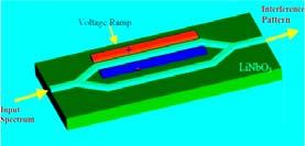
29 Ion Implantation of medium light elements Implanted ions Mask n 1 n 2 Mask n 0 Substrate n 0 Substrate n 1 > n 0 n 1 n 2 < n 0 n 2 n 0 Substrate n 0 Substrate
30 Ion Implantation of medium light elements Damage Profile of a Channel Waveguide realized by High Energy Ion Implantation Au SiO x LiNbO C:LiNbO 3 3.9MeV 6*10 14 at*cm -2 Displaced Atoms (%) n e Depth (µm) Depth (µm)
31 Application: optical modulator Surface Damage LiNbO 3 substrate Implanted channel Substrate End Of Range Damage Mask O 3+ 5MeV Implanted channel waveguide End Of Range Damage How to change the refractive index in one branch? Via the electro-optic effect
32 Electro-optic effect Change in refractive index with the applied electric field: (1/n 2 ) = r E + P E 2 Pockel effect Kerr effect Where: n= Refractive index r = Linear Electro-Optic coefficient P = Quadratic Electro-Optic Coefficient E = Applied Electric Field
33 Electro-optic effect Modulation of the refractive index through the applied electric field Material r (pm/v) n KTP KNbO LiNbO Ba 2 NaNb 5 O l5 SBN (25-75) GaAs BaTiO
34 Ion implantation: application to gas tracing

35 Ion implantation: application to gas tracing LIMB channel White solar light NADIR channel Dispersed gas in the stratosphere Transmitted solar light (without the absorbed wavelenght)

36 Application to gas tracing Input Mach-Zehnder Output Relative Intensity In V Out λ (nm) Different refractive index in the two branches=different phase velocity of the optical beams Reconstruction At the output, beams recombination gives light interference The interference pattern contains the information on the input signal Post analysis of the interference pattern allows the identification of the input signal, i.e gas element


37 Application to gas tracing High selectivity on the wavelength Position of the waveguides below the driving electrodes
38 Nanotech applied to LiNbO 3 Realization of periodic grating acting as wavelength filters LiNbO3 - Aria; 240 nm (50 layers) T R R,T Periodic structure in the nanoscale region obtained by laser irradiation: band pass filter λ (µm)


39 Ion implantation: application in nanotech Ion implantation through a mask Chemical etching on the implanted surface Surface
40 Ion implantation: application in nanotech Effect of the damage on the etching rate MeV O 3+ Implanted LiNbO 3, 1*10 14 at / cm 2 Implanted region are chemically attached faster than unimplanted ones 5000 Depth (Å) Selective etching! 2000 Virgin Material Time (h)


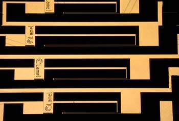
41 Ion implantation: application in nanotech Patterns obtained on LiNbO 3 by ion Implantation and selective etching

42 Ion implantation: application to nanotech Simulation of the electromagnetic field propagation in a Photonic Device obtained by ion implantation + selective etching
43 Perspectives Driving Electrodes waveguide Tunable Mirrors Tunable Resonant Cavity Obtained by periodic structures

44 Outline Resonant Cavity Resonant Cavity, periodicity of the Photonic Structures: 600 nm Photonic Band Gap of the cavity, (Theory)


45 Nanotech applied to LiNbO 3 Laser beam Beam Shaper Mask Projection system Sample 5 µm Lower period can be obtained by laser irradiation
46 Conclusions Ion implantation is a very versatile techinique to modify the LiNbO 3 properties In combination with photolitography it allows for the relaization of optical pattern In principle any complex optical device can be realised, with tailored performances and functionalities
OPTI510R: Photonics. Khanh Kieu College of Optical Sciences, University of Arizona Meinel building R.626
 OPTI510R: Photonics Khanh Kieu College of Optical Sciences, University of Arizona kkieu@optics.arizona.edu Meinel building R.626 Announcements HW#3 is assigned due Feb. 20 st Mid-term exam Feb 27, 2PM
2008,, Jan 7 All-Paid US-Japan Winter School on New Functionalities in Glass. Controlling Light with Nonlinear Optical Glasses and Plasmonic Glasses
 2008,, Jan 7 All-Paid US-Japan Winter School on New Functionalities in Glass Photonic Glass Controlling Light with Nonlinear Optical Glasses and Plasmonic Glasses Takumi FUJIWARA Tohoku University Department
Channel Optical Waveguides with Spatial Longitudinal Modulation of Their Parameters Induced in Photorefractive Lithium Niobate Samples
 Russian Forum of Young Scientists Volume 2018 Conference Paper Channel Optical Waveguides with Spatial Longitudinal Modulation of Their Parameters Induced in Photorefractive Lithium Niobate Samples A D
Multi-cycle THz pulse generation in poled lithium niobate crystals
 Laser Focus World April 2005 issue (pp. 67-72). Multi-cycle THz pulse generation in poled lithium niobate crystals Yun-Shik Lee and Theodore B. Norris Yun-Shik Lee is an assistant professor of physics
Nanocomposite photonic crystal devices
 Nanocomposite photonic crystal devices Xiaoyong Hu, Cuicui Lu, Yulan Fu, Yu Zhu, Yingbo Zhang, Hong Yang, Qihuang Gong Department of Physics, Peking University, Beijing, P. R. China Contents Motivation
12. Nonlinear optics I
 1. Nonlinear optics I What are nonlinear-optical effects and why do they occur? Maxwell's equations in a medium Nonlinear-optical media Second-harmonic generation Conservation laws for photons ("Phasematching")
Potassium Titanyl Phosphate(KTiOPO 4, KTP)
") Potassium Titanyl Phosphate(KTiOPO 4, KTP) Introduction Potassium Titanyl Phosphate (KTiOPO 4 or KTP) is widely used in both commercial and military lasers including laboratory and medical systems, range-finders,
Potassium Titanyl Phosphate(KTiOPO 4, KTP) Introduction Potassium Titanyl Phosphate (KTiOPO 4 or KTP) is widely used in both commercial and military lasers including laboratory and medical systems, range-finders,
Lithium Niobate-On-Insulator (LNOI): Status and Perspectives
: Status and Perspectives") Lithium Niobate-On-Insulator (LNOI): Status and Perspectives Hui Hu (1), Jin Yang (1), Li Gui (2) and Wolfgang Sohler (2) (1) Physics School, Shandong University, 250100, Jinan, P. R. China (2) Department
Lithium Niobate-On-Insulator (LNOI): Status and Perspectives Hui Hu (1), Jin Yang (1), Li Gui (2) and Wolfgang Sohler (2) (1) Physics School, Shandong University, 250100, Jinan, P. R. China (2) Department
3.5x10 8 s/cm (c axis, 22 C, 1KHz) α x =11x10-6 / C, α y =9x10⁻⁶ / C, α z =0.6x10⁻⁶ / C
 α x =11x10-6 / C, α y =9x10⁻⁶ / C, α z =0.6x10⁻⁶ / C") Potassium Titanyl Phosphate (KTiOPO 4 or KTP) KTP (or KTiOPO 4 ) crystal is a nonlinear optical crystal, which possesses excellent nonlinear and electro-optic properties. It has large nonlinear optical
Potassium Titanyl Phosphate (KTiOPO 4 or KTP) KTP (or KTiOPO 4 ) crystal is a nonlinear optical crystal, which possesses excellent nonlinear and electro-optic properties. It has large nonlinear optical
Supplementary Figure 1: SAW transducer equivalent circuit
 Supplementary Figure : SAW transducer equivalent circuit Supplementary Figure : Radiation conductance and susceptance of.6um IDT, experiment & calculation Supplementary Figure 3: Calculated z-displacement
Periodically Poled Lithium Niobate Waveguides for Quantum Frequency Conversion
 Periodically Poled Lithium Niobate Waveguides for Quantum Frequency Conversion J. E. Toney *, V. E. Stenger, A. Pollick, J. Retz, P. Pontius, S. Sriram SRICO, Inc. 2724 Sawbury Boulevard, Columbus, OH
Surface plasmon waveguides
 Surface plasmon waveguides Introduction Size Mismatch between Scaled CMOS Electronics and Planar Photonics Photonic integrated system with subwavelength scale components CMOS transistor: Medium-sized molecule
Nanomaterials and their Optical Applications
 Nanomaterials and their Optical Applications Winter Semester 2012 Lecture 08 rachel.grange@uni-jena.de http://www.iap.uni-jena.de/multiphoton Outline: Photonic crystals 2 1. Photonic crystals vs electronic
Ion Implantation. alternative to diffusion for the introduction of dopants essentially a physical process, rather than chemical advantages:
 Ion Implantation alternative to diffusion for the introduction of dopants essentially a physical process, rather than chemical advantages: mass separation allows wide varies of dopants dose control: diffusion
Optical and Photonic Glasses. Lecture 37. Non-Linear Optical Glasses I - Fundamentals. Professor Rui Almeida
 Optical and Photonic Glasses : Non-Linear Optical Glasses I - Fundamentals Professor Rui Almeida International Materials Institute For New Functionality in Glass Lehigh University Non-linear optical glasses
Transmissive Final Optic for Laser IFE
 Transmissive Final Optic for Laser IFE S. A. Payne, J. F. Latkowski, A. Kubota, M. J. Caturla, S. N. Dixit, and J. A. Speth Lawrence Livermore National Laboratory April 4, 2002 HAPL Program Workshop General
-I (PH 6151) UNIT-V PHOTONICS AND FIBRE OPTICS
 UNIT-V PHOTONICS AND FIBRE OPTICS") Engineering Physics -I (PH 6151) UNIT-V PHOTONICS AND FIBRE OPTICS Syllabus: Lasers Spontaneous and stimulated emission Population Inversion -Einstein s co-efficient (Derivation)- types of lasers-nd-yag,co
Engineering Physics -I (PH 6151) UNIT-V PHOTONICS AND FIBRE OPTICS Syllabus: Lasers Spontaneous and stimulated emission Population Inversion -Einstein s co-efficient (Derivation)- types of lasers-nd-yag,co
Effect of nonlinearity on wave scattering and localization. Yuri S. Kivshar
 Effect of nonlinearity on wave scattering and localization Yuri S. Kivshar Nonlinear Physics Centre, Australian National University, Canberra, Australia St. Petersburg University of Information Technologies,
Optical effects of ion implantation
 Optical effects of ion implantation P. D. TOWNSEND, P. J. CHANDLER and L. ZHANG School of Mathematical and Physical Sciences University of Sussex 1 CAMBRIDGE UNIVERSITY PRESS Preface 1 An overview of ion
Lasers and Electro-optics
 Lasers and Electro-optics Second Edition CHRISTOPHER C. DAVIS University of Maryland III ^0 CAMBRIDGE UNIVERSITY PRESS Preface to the Second Edition page xv 1 Electromagnetic waves, light, and lasers 1
3-1-2 GaSb Quantum Cascade Laser
 3-1-2 GaSb Quantum Cascade Laser A terahertz quantum cascade laser (THz-QCL) using a resonant longitudinal optical (LO) phonon depopulation scheme was successfully demonstrated from a GaSb/AlSb material
Fiber Gratings p. 1 Basic Concepts p. 1 Bragg Diffraction p. 2 Photosensitivity p. 3 Fabrication Techniques p. 4 Single-Beam Internal Technique p.
 Preface p. xiii Fiber Gratings p. 1 Basic Concepts p. 1 Bragg Diffraction p. 2 Photosensitivity p. 3 Fabrication Techniques p. 4 Single-Beam Internal Technique p. 4 Dual-Beam Holographic Technique p. 5
4. Integrated Photonics. (or optoelectronics on a flatland)
") 4. Integrated Photonics (or optoelectronics on a flatland) 1 x Benefits of integration in Electronics: Are we experiencing a similar transformation in Photonics? Mach-Zehnder modulator made from Indium
4. Integrated Photonics (or optoelectronics on a flatland) 1 x Benefits of integration in Electronics: Are we experiencing a similar transformation in Photonics? Mach-Zehnder modulator made from Indium
4. The interaction of light with matter
 4. The interaction of light with matter The propagation of light through chemical materials is described by a wave equation similar to the one that describes light travel in a vacuum (free space). Again,
Study of lithium niobate crystals
 Study of lithium niobate crystals Ekaterina Kochetkova Lomonosov Moscow State University, Russia DESY, Hamburg, Germany September 5, 2017 Abstract This report describes the study of the optical properties
Light Interaction with Small Structures
 Light Interaction with Small Structures Molecules Light scattering due to harmonically driven dipole oscillator Nanoparticles Insulators Rayleigh Scattering (blue sky) Semiconductors...Resonance absorption
Solid State Physics (condensed matter): FERROELECTRICS
: FERROELECTRICS") Solid State Physics (condensed matter): FERROELECTRICS Prof. Igor Ostrovskii The University of Mississippi Department of Physics and Astronomy Oxford, UM: May, 2012 1 People: Solid State Physics Condensed
Solid State Physics (condensed matter): FERROELECTRICS Prof. Igor Ostrovskii The University of Mississippi Department of Physics and Astronomy Oxford, UM: May, 2012 1 People: Solid State Physics Condensed
Defect-based Photonic Crystal Cavity for Silicon Laser
 Defect-based Photonic Crystal Cavity for Silicon Laser Final Term Paper for Nonlinear Optics PHYC/ECE 568 Arezou Khoshakhlagh Instructor: Prof. M. Sheikh-Bahae University of New Mexico karezou@unm.edu
Photonic Crystals. Introduction
 Photonic Crystals Introduction Definition Photonic crystals are new, artificialy created materials, in which refractive index is periodically modulated in a scale compared to the wavelength of operation.
Design of waveguide grating with ultrafast tunable index contrast
 Design of waveguide grating with ultrafast tunable index contrast Sun Do Lim, 1,* In-Kag Hwang, 2 Kwanil Lee, 1 Byoung Yoon Kim, 3 and Sang Bae Lee 1 1 Photonics Sensor System Center, Korea Institute of
Signal regeneration - optical amplifiers
 Signal regeneration - optical amplifiers In any atom or solid, the state of the electrons can change by: 1) Stimulated absorption - in the presence of a light wave, a photon is absorbed, the electron is
Ion Implantation ECE723
 Ion Implantation Topic covered: Process and Advantages of Ion Implantation Ion Distribution and Removal of Lattice Damage Simulation of Ion Implantation Range of Implanted Ions Ion Implantation is the
Refraction and Dispersion in Nonlinear Photonic Crystal Superlattices
 Refraction and Dispersion in Nonlinear Photonic Crystal Superlattices LEOS 18 th Annual Meeting Sydney, Australia Monday, 24 October 2005 Curtis W. Neff, Tsuyoshi Yamashita and Christopher J. Summers Presented
EE 6313 Homework Assignments
 EE 6313 Homework Assignments 1. Homework I: Chapter 1: 1.2, 1.5, 1.7, 1.10, 1.12 [Lattice constant only] (Due Sept. 1, 2009). 2. Homework II: Chapter 1, 2: 1.17, 2.1 (a, c) (k = π/a at zone edge), 2.3
Optics, Optoelectronics and Photonics
 Optics, Optoelectronics and Photonics Engineering Principles and Applications Alan Billings Emeritus Professor, University of Western Australia New York London Toronto Sydney Tokyo Singapore v Contents
Introduction to Photonic Crystals
 1 Introduction to Photonic Crystals Summary. Chapter 1 gives a brief introduction into the basics of photonic crystals which are a special class of optical media with periodic modulation of permittivity.
36. Nonlinear optics: χ(2) processes
 processes") 36. Nonlinear optics: χ() processes The wave equation with nonlinearity Second-harmonic generation: making blue light from red light approximations: SVEA, zero pump depletion phase matching quasi-phase
36. Nonlinear optics: χ() processes The wave equation with nonlinearity Second-harmonic generation: making blue light from red light approximations: SVEA, zero pump depletion phase matching quasi-phase
(b) Spontaneous emission. Absorption, spontaneous (random photon) emission and stimulated emission.
 Spontaneous emission. Absorption, spontaneous (random photon) emission and stimulated emission.") Lecture 10 Stimulated Emission Devices Lasers Stimulated emission and light amplification Einstein coefficients Optical fiber amplifiers Gas laser and He-Ne Laser The output spectrum of a gas laser Laser
Lecture 10 Stimulated Emission Devices Lasers Stimulated emission and light amplification Einstein coefficients Optical fiber amplifiers Gas laser and He-Ne Laser The output spectrum of a gas laser Laser
Interaction of ion beams with matter
 Interaction of ion beams with matter Introduction Nuclear and electronic energy loss Radiation damage process Displacements by nuclear stopping Defects by electronic energy loss Defect-free irradiation
Sub-wavelength electromagnetic structures
 Sub-wavelength electromagnetic structures Shanhui Fan, Z. Ruan, L. Verselegers, P. Catrysse, Z. Yu, J. Shin, J. T. Shen, G. Veronis Ginzton Laboratory, Stanford University http://www.stanford.edu/group/fan
Introduction to semiconductor nanostructures. Peter Kratzer Modern Concepts in Theoretical Physics: Part II Lecture Notes
 Introduction to semiconductor nanostructures Peter Kratzer Modern Concepts in Theoretical Physics: Part II Lecture Notes What is a semiconductor? The Fermi level (chemical potential of the electrons) falls
GRATING CLASSIFICATION
 GRATING CLASSIFICATION SURFACE-RELIEF GRATING TYPES GRATING CLASSIFICATION Transmission or Reflection Classification based on Regime DIFFRACTION BY GRATINGS Acousto-Optics Diffractive Optics Integrated
Introduction to Semiconductor Integrated Optics
 Introduction to Semiconductor Integrated Optics Hans P. Zappe Artech House Boston London Contents acknowledgments reface itroduction Chapter 1 Basic Electromagnetics 1 1.1 General Relationships 1 1.1.1
Theoretical Analysis of the TE Mode Cerenkov Type Second Harmonic Generation in Ion-Implanted X-Cut Lithium Niobate Planar Waveguides
 Vol. 115 (2009) ACTA PHYSICA POLONICA A No. 3 Theoretical Analysis of the TE Mode Cerenkov Type Second Harmonic Generation in Ion-Implanted X-Cut Lithium Niobate Planar Waveguides G. Du, G. Li, S. Zhao,
COMPARISON BETWEEN THE PERFORMANCE OF Ti:LiNbO 3 AND H:LiNbO 3 ROTATED OPTICAL AXIS WAVEGUIDES
 Progress In Electromagnetics Research, PIER 16, 227 267, 1997 COMPARISON BETWEEN THE PERFORMANCE OF Ti:LiNbO 3 AND H:LiNbO 3 ROTATED OPTICAL AXIS WAVEGUIDES F. Prudenzano, A. D Orazio, V. Petruzzelli,
PRINCIPLES OF PHYSICAL OPTICS
 PRINCIPLES OF PHYSICAL OPTICS C. A. Bennett University of North Carolina At Asheville WILEY- INTERSCIENCE A JOHN WILEY & SONS, INC., PUBLICATION CONTENTS Preface 1 The Physics of Waves 1 1.1 Introduction
What do we study and do?
 What do we study and do? Light comes from electrons transitioning from higher energy to lower energy levels. Wave-particle nature of light Wave nature: refraction, diffraction, interference (labs) Particle
Introduction to Nonlinear Optics
 Introduction to Nonlinear Optics Prof. Cleber R. Mendonca http://www.fotonica.ifsc.usp.br Outline Linear optics Introduction to nonlinear optics Second order nonlinearities Third order nonlinearities Two-photon
Segmented 1.55um Laser with 400% Differential Quantum Efficiency J. Getty, E. Skogen, L. Coldren, University of California, Santa Barbara, CA.
 Segmented 1.55um Laser with 400% Differential Quantum Efficiency J. Getty, E. Skogen, L. Coldren, University of California, Santa Barbara, CA. Abstract: By electrically segmenting, and series-connecting
Photorefractive Waveguides
 Gunter / Photorefractive Materials and their Applications 1 chap10 Revise Proof page 289 22.8.2005 4:23pm 10 Photorefractive Waveguides Detlef Kip 1 and Monika Wesner 2 1 Institute of Physics and Physical
Oscillateur paramétrique optique en
 C. Ozanam 1, X. Lafosse 2, I. Favero 1, S. Ducci 1, G. Leo 1 1 Université Paris Diderot, Sorbonne Paris Cité, Laboratoire MPQ, CNRS-UMR 7162, Paris, France, 2 Laboratoire de Photonique et Nanostructures,
SURFACE ACOUSTIC WAVE FERROELECTRIC PHONONIC CRYSTAL TUNABLE BY ELECTRIC FIELD
 NANOSYSTEMS: PHYSICS, CHEMISTRY, MATHEMATICS, 2013, 4 (5), P. 630 634 SURFACE ACOUSTIC WAVE FERROELECTRIC PHONONIC CRYSTAL TUNABLE BY ELECTRIC FIELD V. P. Pashchenko 1,2 1 Saint Petersburg State Polytechnical
Chapter 5. Semiconductor Laser
 Chapter 5 Semiconductor Laser 5.0 Introduction Laser is an acronym for light amplification by stimulated emission of radiation. Albert Einstein in 1917 showed that the process of stimulated emission must
A tutorial on meta-materials and THz technology
 p.1/49 A tutorial on meta-materials and THz technology Thomas Feurer thomas.feurer@iap.unibe.ch Institute of Applied Physics Sidlerstr. 5, 3012 Bern Switzerland p.2/49 Outline Meta-materials Super-lenses
Nonlinear Optics (NLO)
") Nonlinear Optics (NLO) (Manual in Progress) Most of the experiments performed during this course are perfectly described by the principles of linear optics. This assumes that interacting optical beams
Nonlinear Optics (NLO) (Manual in Progress) Most of the experiments performed during this course are perfectly described by the principles of linear optics. This assumes that interacting optical beams
Gratings in Electrooptic Polymer Devices
 Gratings in Electrooptic Polymer Devices Venkata N.P.Sivashankar 1, Edward M. McKenna 2 and Alan R.Mickelson 3 Department of Electrical and Computer Engineering, University of Colorado at Boulder, Boulder,
Chapter 7: Optical Properties of Solids. Interaction of light with atoms. Insert Fig Allowed and forbidden electronic transitions
 Chapter 7: Optical Properties of Solids Interaction of light with atoms Insert Fig. 8.1 Allowed and forbidden electronic transitions 1 Insert Fig. 8.3 or equivalent Ti 3+ absorption: e g t 2g 2 Ruby Laser
Stimulated Emission Devices: LASERS
 Stimulated Emission Devices: LASERS 1. Stimulated Emission and Photon Amplification E 2 E 2 E 2 hυ hυ hυ In hυ Out hυ E 1 E 1 E 1 (a) Absorption (b) Spontaneous emission (c) Stimulated emission The Principle
Temperature Tuning Characteristics of Periodically Poled Lithium Niobate for Second Harmonic Generation at 490 nm
 Temperature Tuning Characteristics of Periodically Poled Lithium Niobate for Second Harmonic Generation at 490 nm Movva Sai Krishna *a, U.S. Tripathi a, Ashok Kaul a, K. Thyagarajan b, M.R. Shenoy b a
Helium-ion-induced radiation damage in LiNbO 3 thin-film electro-optic modulators
 Helium-ion-induced radiation damage in LiNbO 3 thin-film electro-optic modulators Hsu-Cheng Huang, 1,* Jerry I. Dadap, 2 Girish Malladi, 3 Ioannis Kymissis, 1 Hassaram Bakhru, 3 and Richard M. Osgood,
Self-study problems and questions Processing and Device Technology, FFF110/FYSD13
 Self-study problems and questions Processing and Device Technology, FFF110/FYSD13 Version 2016_01 In addition to the problems discussed at the seminars and at the lectures, you can use this set of problems
Laser Basics. What happens when light (or photon) interact with a matter? Assume photon energy is compatible with energy transition levels.
 interact with a matter? Assume photon energy is compatible with energy transition levels.") What happens when light (or photon) interact with a matter? Assume photon energy is compatible with energy transition levels. Electron energy levels in an hydrogen atom n=5 n=4 - + n=3 n=2 13.6 = [ev]
What happens when light (or photon) interact with a matter? Assume photon energy is compatible with energy transition levels. Electron energy levels in an hydrogen atom n=5 n=4 - + n=3 n=2 13.6 = [ev]
Photonic Band Gap Crystals. Srivatsan Balasubramanian
 Photonic Band Gap Crystals Srivatsan Balasubramanian Summary Physics of photonic bandgap crystals. Photonic Crystals Classification. Fabrication. Applications. Protoype photonic band gap devices. Current
Quadratic nonlinear interaction
 Nonlinear second order χ () interactions in III-V semiconductors 1. Generalities : III-V semiconductors & nd ordre nonlinear optics. The strategies for phase-matching 3. Photonic crystals for nd ordre
II-VI semiconductor nano-crystal quantum dots and electro-optic active polymers,
 CHAPTER 1 Introduction II-VI semiconductor nano-crystal quantum dots and electro-optic active polymers, which exhibit electro-optic and nonlinear optical properties different from those of corresponding
Chapter 3 Chapter 4 Chapter 5
 Preamble In recent years bismuth-based, layer-structured perovskites such as SrBi 2 Nb 2 O 9 (SBN) and SrBi 2 Ta 2 O 9 (SBT) have been investigated extensively, because of their potential use in ferroelectric
Introduction to Optoelectronic Device Simulation by Joachim Piprek
 NUSOD 5 Tutorial MA Introduction to Optoelectronic Device Simulation by Joachim Piprek Outline:. Introduction: VCSEL Example. Electron Energy Bands 3. Drift-Diffusion Model 4. Thermal Model 5. Gain/Absorption
ECE 484 Semiconductor Lasers
 ECE 484 Semiconductor Lasers Dr. Lukas Chrostowski Department of Electrical and Computer Engineering University of British Columbia January, 2013 Module Learning Objectives: Understand the importance of
Nonlinear Optics and Gap Solitons in Periodic Photonic Structures
 Nonlinear Optics and Gap Solitons in Periodic Photonic Structures Yuri Kivshar Nonlinear Physics Centre Research School of Physical Sciences and Engineering Australian National University Perspectives
PHYSICS nd TERM Outline Notes (continued)
") PHYSICS 2800 2 nd TERM Outline Notes (continued) Section 6. Optical Properties (see also textbook, chapter 15) This section will be concerned with how electromagnetic radiation (visible light, in particular)
PHYSICS 2800 2 nd TERM Outline Notes (continued) Section 6. Optical Properties (see also textbook, chapter 15) This section will be concerned with how electromagnetic radiation (visible light, in particular)
Surface analysis techniques
 Experimental methods in physics Surface analysis techniques 3. Ion probes Elemental and molecular analysis Jean-Marc Bonard Academic year 10-11 3. Elemental and molecular analysis 3.1.!Secondary ion mass
Nanomaterials and their Optical Applications
 Nanomaterials and their Optical Applications Winter Semester 2013 Lecture 02 rachel.grange@uni-jena.de http://www.iap.uni-jena.de/multiphoton Lecture 2: outline 2 Introduction to Nanophotonics Theoretical
Optical and Photonic Glasses. Lecture 39. Non-Linear Optical Glasses III Metal Doped Nano-Glasses. Professor Rui Almeida
 Optical and Photonic Glasses : Non-Linear Optical Glasses III Metal Doped Nano-Glasses Professor Rui Almeida International Materials Institute For New Functionality in Glass Lehigh University Metal-doped
Diode Lasers and Photonic Integrated Circuits
 Diode Lasers and Photonic Integrated Circuits L. A. COLDREN S. W. CORZINE University of California Santa Barbara, California A WILEY-INTERSCIENCE PUBLICATION JOHN WILEY & SONS, INC. NEW YORK / CHICHESTER
Liquid Crystals IAM-CHOON 1(1100 .,4 WILEY 2007 WILEY-INTERSCIENCE A JOHN WILEY & SONS, INC., PUBLICATION. 'i; Second Edition. n z
 Liquid Crystals Second Edition IAM-CHOON 1(1100.,4 z 'i; BICENTCNNIAL 1 8 0 7 WILEY 2007 DICENTENNIAL n z z r WILEY-INTERSCIENCE A JOHN WILEY & SONS, INC., PUBLICATION Contents Preface xiii Chapter 1.
The Electromagnetic Properties of Materials
 The Electromagnetic Properties of Materials Electrical conduction Metals Semiconductors Insulators (dielectrics) Superconductors Magnetic materials Ferromagnetic materials Others Photonic Materials (optical)
what happens if we make materials smaller?
 what happens if we make materials smaller? IAP VI/10 ummer chool 2007 Couvin Prof. ns outline Introduction making materials smaller? ynthesis how do you make nanomaterials? Properties why would you make
In situ TEM studies of helium bubble/platelet evolution in Si based materials
 In situ TEM studies of helium bubble/platelet evolution in Si based materials M. Vallet 1, M.F. Beaufort 1, J.F. Barbot 1, E. Oliviero 2 and S.E. Donnelly 3 1 Institut Pprime, CNRS-Université de Poitiers,
Ultra-Slow Light Propagation in Room Temperature Solids. Robert W. Boyd
 Ultra-Slow Light Propagation in Room Temperature Solids Robert W. Boyd The Institute of Optics and Department of Physics and Astronomy University of Rochester, Rochester, NY USA http://www.optics.rochester.edu
Electromagnetic Metamaterials
 Photonic Bandgap and Electromagnetic Metamaterials Andrew Kirk andrew.kirk@mcgill.ca ca Department of Electrical and Computer Engineering McGill Institute for Advanced Materials A Kirk 11/24/2008 Photonic
Metal Vapour Lasers Use vapoured metal as a gain medium Developed by W. Silfvast (1966) Two types: Ionized Metal vapour (He-Cd) Neutral Metal vapour
 Two types: Ionized Metal vapour (He-Cd) Neutral Metal vapour") Metal Vapour Lasers Use vapoured metal as a gain medium Developed by W. Silfvast (1966) Two types: Ionized Metal vapour (He-Cd) Neutral Metal vapour (Cu) All operate by vaporizing metal in container Helium
Metal Vapour Lasers Use vapoured metal as a gain medium Developed by W. Silfvast (1966) Two types: Ionized Metal vapour (He-Cd) Neutral Metal vapour (Cu) All operate by vaporizing metal in container Helium
Fabrication Technology, Part I
 EEL5225: Principles of MEMS Transducers (Fall 2004) Fabrication Technology, Part I Agenda: Microfabrication Overview Basic semiconductor devices Materials Key processes Oxidation Thin-film Deposition Reading:
Quantum Microwave Photonics:
 Quantum Microwave Photonics:Coupling quantum microwave circuits to quantum optics via cavity electro-optic modulators p. 1/16 Quantum Microwave Photonics: Coupling quantum microwave circuits to quantum
QUESTION BANK IN PHYSICS
 QUESTION BANK IN PHYSICS LASERS. Name some properties, which make laser light different from ordinary light. () {JUN 5. The output power of a given laser is mw and the emitted wavelength is 630nm. Calculate
Electro-optic and electro-absorption characterization of InAs quantum dot waveguides
 Electro-optic and electro-absorption characterization of InAs quantum dot waveguides Imran B. Akca, 1,* Aykutlu Dâna, 1 Atilla Aydinli, 1 Marco Rossetti, 2 Lianhe Li, 2 Andrea Fiore, 2 and Nadir Dagli
Fast Monte-Carlo Simulation of Ion Implantation. Binary Collision Approximation Implementation within ATHENA
 Fast Monte-Carlo Simulation of Ion Implantation Binary Collision Approximation Implementation within ATHENA Contents Simulation Challenges for Future Technologies Monte-Carlo Concepts and Models Atomic
Time Domain Modeling of All-Optical Switch based on PT-Symmetric Bragg Grating
 Time Domain Modeling of All-Optical Switch based on PT-Symmetric Bragg Grating Sendy Phang 1, Ana Vukovic 1, Hadi Susanto 2, Trevor M. Benson 1, and Phillip Sewell 1 1 School of Electrical and Electronic
CHAPTER 7 SUMMARY OF THE PRESENT WORK AND SUGGESTIONS FOR FUTURE WORK
 161 CHAPTER 7 SUMMARY OF THE PRESENT WORK AND SUGGESTIONS FOR FUTURE WORK 7.1 SUMMARY OF THE PRESENT WORK Nonlinear optical materials are required in a wide range of important applications, such as optical
Laser Physics OXFORD UNIVERSITY PRESS SIMON HOOKER COLIN WEBB. and. Department of Physics, University of Oxford
 Laser Physics SIMON HOOKER and COLIN WEBB Department of Physics, University of Oxford OXFORD UNIVERSITY PRESS Contents 1 Introduction 1.1 The laser 1.2 Electromagnetic radiation in a closed cavity 1.2.1
Lecture 15: Optoelectronic devices: Introduction
 Lecture 15: Optoelectronic devices: Introduction Contents 1 Optical absorption 1 1.1 Absorption coefficient....................... 2 2 Optical recombination 5 3 Recombination and carrier lifetime 6 3.1
Slowdown of group velocity of light in PPLN by employing electro-optic effect
 Journal of Nonlinear Optical Physics & Materials Vol. 23, No. 1 (2014) 1450006 (8 pages) c World Scientific Publishing Company DOI: 10.1142/S0218863514500064 Slowdown of group velocity of light in PPLN
Propagation of Photons Through Localized Coupled Cavity Modes in Photonic Band Gap Structures:
 CLEO, May 7-12, 7 2000, San Francisco Propagation of Photons Through Localized Coupled Cavity Modes in Photonic Band Gap Structures: A New Type of Waveguiding Mechanism Mehmet Bayındır Burak Temelkuran
Silicon Photonics Technology for Advanced Computing Applications
 Silicon Photonics Technology for Advanced Computing Applications Bert Jan Offrein Dresden, March 23, 2018 Neuromorphic Devices and Systems Group 2016 IBM Corporation Outline Photonics and computing? The
MP5: Soft Matter: Physics of Liquid Crystals
 MP5: Soft Matter: Physics of Liquid Crystals 1 Objective In this experiment a liquid crystal display (LCD) is built and its functionality is tested. The light transmission as function of the applied voltage
Research Article Domain-Reversed Lithium Niobate Single-Crystal Fibers are Potentially for Efficient Terahertz Wave Generation
 Advances in OptoElectronics Volume 008, Article ID 08458, 5 pages doi:10.1155/008/08458 Research Article Domain-Reversed Lithium Niobate Single-Crystal Fibers are Potentially for Efficient Terahertz Wave
Non-traditional methods of material properties and defect parameters measurement
 Non-traditional methods of material properties and defect parameters measurement Juozas Vaitkus on behalf of a few Vilnius groups Vilnius University, Lithuania Outline: Definition of aims Photoconductivity
Diffusione nei solidi: teoria e applicazioni a materiali avanzati
 Università Ca Foscari Venezia Diffusione nei solidi: teoria e applicazioni a materiali avanzati Prof. Elti Cattaruzza Department of Molecular Sciences and Nanosystems, Università Ca Foscari Venezia, via
Solitons. Nonlinear pulses and beams
 Solitons Nonlinear pulses and beams Nail N. Akhmediev and Adrian Ankiewicz Optical Sciences Centre The Australian National University Canberra Australia m CHAPMAN & HALL London Weinheim New York Tokyo
TUNABLE MULTI-CHANNEL FILTERING USING 1-D PHOTONIC QUANTUM WELL STRUCTURES
 Progress In Electromagnetics Research Letters, Vol. 27, 43 51, 2011 TUNABLE MULTI-CHANNEL FILTERING USING 1-D PHOTONIC QUANTUM WELL STRUCTURES B. Suthar * and A. Bhargava Nanophysics Laboratory, Department
Doctor of Philosophy
 FEMTOSECOND TIME-DOMAIN SPECTROSCOPY AND NONLINEAR OPTICAL PROPERTIES OF IRON-PNICTIDE SUPERCONDUCTORS AND NANOSYSTEMS A Thesis Submitted for the degree of Doctor of Philosophy IN THE FACULTY OF SCIENCE