Nanostrutture con funzionalità avanzate
|
|
|
- Jordan Little
- 6 years ago
- Views:
Transcription
1 Unità di Ricerca 4 Nanostrutture con funzionalità avanzate Progettazione, simulazione e test di componenti planari per optoelettronica, compatibili con la tecnologia CMOS (cristalli fotonici, guide d onda, sorgenti laser, risonatori, specchi dielettrici, filtri, amplificatori, ) Studio di fattibilità di prototipi e nuovi dispositivi (attivi o passivi) optoelettronici e fotonici (quali commutatori e transistor ottici) che possano essere integrati su moduli multi-chip o a singolo CMOS- chip.

2 Integrated Silicon Nanophotonics Futuristic Silicon chip with integrated photonic and electronic circuits IBM Research, (2007) The ultimate goal of Si nanophotonics is to develop a technology for on-chip integration of ultra-compact nanophotonic circuits for manipulating the light signals, similar to the way electrical signals are manipulated in a computer chip
3 Integrated Silicon Nanophotonics The interconnection bottleneck RC delay: speed Microwave Crosstalk Heat/power issue

4 Integrated Silicon Nanophotonics An electron/photon convergence Long haul telecommunications Microelectronics IC chip

5 Integrated Silicon Nanophotonics Application: on-chip optical clock distribution
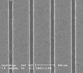
6 Optical waveguides for Si nanophotonics Wires for electrons, waveguides for photons n 1 n 1 =1 n 2 > n 1, n 3 n 3 Substrate Planar dielectric waveguide Light is transported in-plane losslessly by total internal reflection at the wg interfaces Loss, dispersion Planar integration (CMOS) Waveguides for the silicon platform: - Silica, SiON, Si 3 N 4, poly-si, a-si, SOI
")
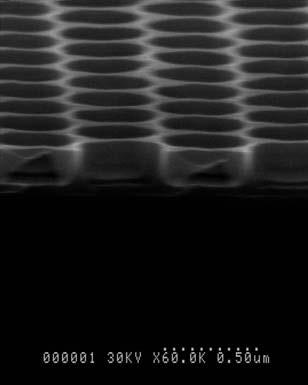
7 Progetto FIRB - WP5 Silicon-On-Insulator (SOI) waveguides SOI platform Si photonic wires air Si SiO 2 n 1 = n 1=1 n 2 = 3.5 n 3 =1.45 Si Fabricated by SOITEC, up to 12 inch wafers High dielectric contrast Fully CMOS compatibility Processable with standard CMOS technology (electron beam/optical lithography & reactive ion etching) Propagation losses < 3 db/cm Y. Vlasov et al. Optics Express 12, 1622 (2004)


8 Bends and Splits Routing the light on the chip Silicon photonic wires with µ bends Bend radius R = 5 µm Loss = db/bend Silicon photonic wires with µ splits 90 : loss = 2.7 db/split 15 : loss = 0.7 db/split Y. Vlasov et al. Optics Express 12, 1622 (2004)

9 Silicon Nanophotonics Si potonics scaling in 2 decades: Higher refractive index contrast = smaller bending radius = higher integration density IBM Research, (2007)
10 Photonic Crystal Waveguides
11 Progetto FIRB - WP5 Photonic crystals ω ω = k ε 1 Uniform medium ε 1 0 ω Add a small real periodicity ε 2 = ε 1 + ε k sin π a x a ε (x) = ε (x+a) ε 1 ε 2 ε 1 ε 2 ε 1 ε 2 ε 1 ε 2 ε 1 ε 2 ε 1 ε 2 band gap cos π a x 0 π/a
12 Progetto FIRB - WP5 Photonic Crystals Strong modification of the dispersion relation with scale invariance! frequency photonic band gap backwards slope: negative refraction dω/dk 0: slow light wavevector strong dispersion: super-prism effect + negative refraction


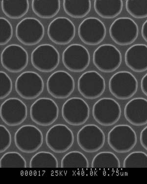

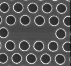
13 Progetto FIRB - WP5 SOI Photonic crystal slabs one-dimensional two-dimensional membrane W1 line defects with line-defects with point -defects Ridge Waveguides 6 µm membrane

 PhC bends &")

14 SOI photonic crystal waveguides, bends & splits PhC straight wg Propagation Loss ~ 3 db/cm Y. Vlasov et al. Optics Express 11, 2927 (2003) PhC bends & splits Bend Loss ~ 0.05 db/bend Split Loss ~ 3 db/split Y. Vlasov et al. Optics Letters 31, 745 (2003)

15 Optical Spectroscopy tools for nanophotonics FT spectrometer + white light source spectral range for transmission/emission µm Tunable Laser source: µm (spectral resolution 2 pm)
 oxide (BPSG) Coll. with Univ.")
 -3-4 -5-6 Transmission (db) -2-4 -6-8 -10 0.73 db/cm 4.")
 -7 0.0 0.5 1.0 1.5 2.0 2.5 3.0 Length (cm) -7 0.0 0.5 1.0 1.5 2.0 2.5 3.0 Length (cm) -8 0.")
16 Propagation Loss Spectra of Si 3 N 4 /SiO 2 waveguides nm 500 nm 200 nm 2000 nm Si 3 N 4 oxide (SiO 2 ) oxide (BPSG) Coll. with Univ. Trento IRST-ITC Cut-back Si TE polarization TM polarization db/cm db/cm Loss (db/cm) Transmission (db) db/cm 4.7 db/cm 1544 nm 780 nm 532 nm Transmission(dB) db/cm 5.7 db/cm 1200 nm 780 nm 532 nm Loss (db/cm) Length (cm) Length (cm) Wavelength (µm) Wavelength (µm)

 TE Polarization 0.7 0.0 0.2 0.4 0.6 0.8 1.0 Transmittance σ kz = +1 0.")
17 Progetto FIRB - WP5 Waveguide Transmission on SOI 2D PhC structures 5 µm Energy (ev) triangular array of air holes GK a = 400 GM Γ Κ nm; r/a = 0.34 TE Polarization Γ Μ TE-like TM-like Energy (ev) Trasmittance Μ Γ Κ µm Energy (ev) W1.5 σ kz = Energy (ev) TE Polarization Transmittance σ kz = k x a/π
18 Attenuated Total Reflection spectroscopy on SOI wg ATR spectroscopy 2,0 2,0 Evanescent coupling to guided modes 1,5 TM exp. TE exp. TM calc. TE calc. 1,5 θ ZnSe, Si Energy (ev) 1,0 1,0 Si core Air layer SiO 2 cladding ω sin ( ), c n k = prism θ ω 0,5 0, βd SOI slab d S = 0 nm, d = 270 nm 0,5 1,5 2,0 2,5 3,0 0,0 n eff Direct measure of the guided mode dispersion M. Galli et al., Appl. Phys. Lett. 89, (2006)


19 ATR on single line-defect PhC waveguides W1 line-defect 0,92 0,90 0,92 0,90 3a Energy (ev) Energy (ev) W1.5 line-defect 1.5 3a 0,88 0,86 0,84 0,82 0,80 0,78 0,92 0,90 0,88 0,86 0,84 0,82 0,80 0,78 θ=55 θ=55 ATR W1.0 φ = 0 θ=39 W1.5 φ = 0 θ=40 θ=60 θ=60 ATR W1.0 W1.0 φ = 15 θ=43 W1.5 φ = 15 θ=38 0,88 0,86 0,84 σ kz = 1 0,82 σ kz = +1 0,80 0,78 0,92 0,90 W1.5 0,88 0,86 0,84 0,82 σ kz = 1 0,80 σ kz = +1 0, k x a/π M. Galli et al., Physical Review B 72, (2005)


20 Application: chip to chip? Clocking Chip to chip connections - Filters - Modulators - Light sources v


21 Planar Optical Microcavities Si ring resonators PhC cavities Q factor ~ 5 x 10 4 Q factor ~ 2 x 10 5
 1dB band pass: 310 GHz Out of band rejection: 40")
22 Ultra-small high-order optical filters Insertion loss: 1.8 db Y. Vlasov et al. Optics Express 15, (2007) 1dB band pass: 310 GHz Out of band rejection: 40 db


23 Photonic crystal add/drop filters The transmission frequency range of the output waveguide with bends is tuned by changing the size of the air holes at the apex of the corner. Noda et al. Appl. Phys. Lett. 84, 2226 (2004)


24 Encoding a channel: modulation Micrometer-scale Si electro-optic modulator Electrically driven by a p-i-n junction integrated with the ring resonator ~ 1 Gbit/s modulation speed with high modulation depth Only 12 µm footprint! Lipson et al., Nature 435, 325 (2005)


25 All-optical switching on a silicon chip optical bistability Notomi et al., Opt. Expr. 13, 2678 (2005)
26 Progetto FIRB - WP5 All-optical switching in silicon PhCs All-optical switching experiment at our Lab. (Pavia)

27 All-optical switching in silicon PhCs Tunable Laser source: µm (spectral resolution 2 pm)
 0-5 -10 1397.12 nm cw-probe -15-5 0 5 10 15 20 Time (ns) λ =1397.12 0.00 0.880 0.885 0.890 0.895 0.")
28 Progetto FIRB - WP5 All-optical switching in silicon PhCs PhC cavity Signal Intensity (a.u.) 0,6 0,4 0,2 532 nm Pulsed Pump 0,0 Signal (V) E = 160 µev Q = Transmission (db) nm cw-probe Time (ns) λ = Energy (ev) Switching power ~ 140 nw

 Paniccia et al.")
29 Active Si nanophotonics Light Sources & Waveguide Optical Amplifiers Challenge: CMOS integration Challenge: electrical injection Si Raman Laser Hybrid Si Laser InP wg Silicon Paniccia et al., Intel (2006) Paniccia et al., Intel (2006)


30 Active PhC based on III-V semiconductors Ultra low-threshold lasing in PhC nanocavities S. Strauf, L.C. Andreani et al., PRL 96, (2006)

31 Progetto FIRB - WP5 Optically active Silicon Doping with Si-nanocrystals and rare earth ions (Er 3+ ) Si-nanocrystals act as a very efficient Er-sensitizers for excitation by means of energy transfer process A. Polman, Nature Materials 1, 10 (2002)


 Er-doped SiO x Si")
32 Progetto FIRB - WP5 Active Silicon-On-Insulator waveguides Si core Active layer: Si-nc:Er:SiO 2 d S = nm Multilayer deposition by radiofrequency confocal magnetron sputtering (T=300K) Er-doped SiO x Si 37 at. % Er 3.8x nm
 L = 0.35 mm Microscope objective Pump beam WD >> L L L = 0.15 mm TM TE 0.0 0.75 0.80 0.85 0.90 Energy (ev) M. Galli et al.")
33 Progetto FIRB - WP5 High field-confining SOI waveguides Very efficient light emission from a 20 nm-thick only active layer PL Intensity (a.u.) TM/TE ratio Distance from edge (mm) L = 0.35 mm Microscope objective Pump beam WD >> L L L = 0.15 mm TM TE Energy (ev) M. Galli et al., Appl. Phys. Lett. 89, (2006)

 Κ PL intensity (arb. units) 0.4 0.3 PhC, a=1070 nm PhC, a=1210 nm 0.")
34 Active silicon-on-insulator PhC slabs 0.85 Γ Κ Γ Μ 1070 nm Careful PhC deisgn Resonance of Er 3+ emission with a photonic mode 150-fold enhancement of emission 0.5 Er 3+ emission (a/λ) Μ Γ calc TM calc TE M. Galli et al., Appl. Phys. Lett. 88, (2006) Κ PL intensity (arb. units) PhC, a=1070 nm PhC, a=1210 nm 0.2 Unpatterned SOI 0.1 (x 5) Energy (ev) Reflectance (arb. units)


35 Progetto FIRB - WP5 Integrated light-emitting devices Electrical contacts n + poly Si n SiO + poly x :ErSi 3+ p + poly SiOSi x p + Si SiO µm A. Irrera et al., Nanotechnology 17, 1248 (2006)
36 Progetto FIRB - WP5 Task activities SOI Photonic crystal waveguides High-Q photonic crystal cavities All-optical switching in SOI PhC structures Active SOI waveguides and cavities Optical characterization and testing Waveguide transmission spectroscopy Angle-resolved reflectance and ATR spectroscopy Photoluminescence spectroscopy Theory and Design Photonic bands Propagation losses Cavity Q factors Emission properties Effect of disorder Device design
Surface plasmon waveguides
 Surface plasmon waveguides Introduction Size Mismatch between Scaled CMOS Electronics and Planar Photonics Photonic integrated system with subwavelength scale components CMOS transistor: Medium-sized molecule
Photonic Crystal Nanocavities for Efficient Light Confinement and Emission
 Journal of the Korean Physical Society, Vol. 42, No., February 2003, pp. 768 773 Photonic Crystal Nanocavities for Efficient Light Confinement and Emission Axel Scherer, T. Yoshie, M. Lončar, J. Vučković
OPTI510R: Photonics. Khanh Kieu College of Optical Sciences, University of Arizona Meinel building R.626
 OPTI510R: Photonics Khanh Kieu College of Optical Sciences, University of Arizona kkieu@optics.arizona.edu Meinel building R.626 Announcements HW#3 is assigned due Feb. 20 st Mid-term exam Feb 27, 2PM
Electromagnetic Metamaterials
 Photonic Bandgap and Electromagnetic Metamaterials Andrew Kirk andrew.kirk@mcgill.ca ca Department of Electrical and Computer Engineering McGill Institute for Advanced Materials A Kirk 11/24/2008 Photonic
4. Integrated Photonics. (or optoelectronics on a flatland)
") 4. Integrated Photonics (or optoelectronics on a flatland) 1 x Benefits of integration in Electronics: Are we experiencing a similar transformation in Photonics? Mach-Zehnder modulator made from Indium
4. Integrated Photonics (or optoelectronics on a flatland) 1 x Benefits of integration in Electronics: Are we experiencing a similar transformation in Photonics? Mach-Zehnder modulator made from Indium
Advanced techniques Local probes, SNOM
 Advanced techniques Local probes, SNOM Principle Probe the near field electromagnetic field with a local probe near field probe propagating field evanescent Advanced techniques Local probes, SNOM Principle
Appendix. Photonic crystal lasers: future integrated devices
 91 Appendix Photonic crystal lasers: future integrated devices 5.1 Introduction The technology of photonic crystals has produced a large variety of new devices. However, photonic crystals have not been
Simulations of nanophotonic waveguides and devices using COMSOL Multiphysics
 Presented at the COMSOL Conference 2010 China Simulations of nanophotonic waveguides and devices using COMSOL Multiphysics Zheng Zheng Beihang University 37 Xueyuan Road, Beijing 100191, China Acknowledgement
SUPPLEMENTARY INFORMATION
 doi:10.1038/nature12036 We provide in the following additional experimental data and details on our demonstration of an electrically pumped exciton-polariton laser by supplementing optical and electrical
Signal regeneration - optical amplifiers
 Signal regeneration - optical amplifiers In any atom or solid, the state of the electrons can change by: 1) Stimulated absorption - in the presence of a light wave, a photon is absorbed, the electron is
Nanomaterials and their Optical Applications
 Nanomaterials and their Optical Applications Winter Semester 2012 Lecture 08 rachel.grange@uni-jena.de http://www.iap.uni-jena.de/multiphoton Outline: Photonic crystals 2 1. Photonic crystals vs electronic
Photonic devices for quantum information processing:
 Outline Photonic devices for quantum information processing: coupling to dots, structure design and fabrication Optoelectronics Group, Cavendish Lab Outline Vuckovic s group Noda s group Outline Outline
High speed modulation of hybrid silicon evanescent lasers
 High speed modulation of hybrid silicon evanescent lasers Daoxin Dai, AW Fang and John E Bowers University of California anta Barbara, ECE Department, anta Barbara, CA 936, UA dxdai@ece.ucsb.edu This research
Refraction and Dispersion in Nonlinear Photonic Crystal Superlattices
 Refraction and Dispersion in Nonlinear Photonic Crystal Superlattices LEOS 18 th Annual Meeting Sydney, Australia Monday, 24 October 2005 Curtis W. Neff, Tsuyoshi Yamashita and Christopher J. Summers Presented
Surface-Plasmon Sensors
 Surface-Plasmon Sensors Seok Ho Song Physics Department in Hanyang University Dongho Shin, Jaewoong Yun, Kihyong Choi Gwansu Lee, Samsung Electro-Mechanics Contents Dispersion relation of surface plasmons
Investigation on Mode Splitting and Degeneracy in the L3 Photonic Crystal Nanocavity via Unsymmetrical Displacement of Air-Holes
 The International Journal Of Engineering And Science (Ijes) Volume 2 Issue 2 Pages 146-150 2013 Issn: 2319 1813 Isbn: 2319 1805 Investigation on Mode Splitting and Degeneracy in the L3 Photonic Crystal
Plasmonic nanoguides and circuits
 Plasmonic nanoguides and circuits Introduction: need for plasmonics? Strip SPPs Cylindrical SPPs Gap SPP waveguides Channel plasmon polaritons Dielectric-loaded SPP waveguides PLASMOCOM 1. Intro: need
Inhibited and Enhanced Spontaneous Emission from Quantum Dots using 2D Silicon-Based Photonic Crystal Waveguides
 Inhibited and Enhanced Spontaneous Emission from Quantum Dots using 2D Silicon-Based Photonic Crystal Waveguides W. Amorntep and P. Wanchai Quantum Information and Computing Development Research Group
Laser Basics. What happens when light (or photon) interact with a matter? Assume photon energy is compatible with energy transition levels.
 interact with a matter? Assume photon energy is compatible with energy transition levels.") What happens when light (or photon) interact with a matter? Assume photon energy is compatible with energy transition levels. Electron energy levels in an hydrogen atom n=5 n=4 - + n=3 n=2 13.6 = [ev]
What happens when light (or photon) interact with a matter? Assume photon energy is compatible with energy transition levels. Electron energy levels in an hydrogen atom n=5 n=4 - + n=3 n=2 13.6 = [ev]
Light Interaction with Small Structures
 Light Interaction with Small Structures Molecules Light scattering due to harmonically driven dipole oscillator Nanoparticles Insulators Rayleigh Scattering (blue sky) Semiconductors...Resonance absorption
Design of a Multi-Mode Interference Crossing Structure for Three Periodic Dielectric Waveguides
 Progress In Electromagnetics Research Letters, Vol. 75, 47 52, 2018 Design of a Multi-Mode Interference Crossing Structure for Three Periodic Dielectric Waveguides Haibin Chen 1, Zhongjiao He 2,andWeiWang
Nanocomposite photonic crystal devices
 Nanocomposite photonic crystal devices Xiaoyong Hu, Cuicui Lu, Yulan Fu, Yu Zhu, Yingbo Zhang, Hong Yang, Qihuang Gong Department of Physics, Peking University, Beijing, P. R. China Contents Motivation
Introduction to Photonic Crystals
 1 Introduction to Photonic Crystals Summary. Chapter 1 gives a brief introduction into the basics of photonic crystals which are a special class of optical media with periodic modulation of permittivity.
Polariton laser in micropillar cavities
 Polariton laser in micropillar cavities D. Bajoni, E. Wertz, P. Senellart, I. Sagnes, S. Bouchoule, A. Miard, E. Semenova, A. Lemaître and J. Bloch Laboratoire de Photonique et de Nanostructures LPN/CNRS,
FINITE-DIFFERENCE FREQUENCY-DOMAIN ANALYSIS OF NOVEL PHOTONIC
 FINITE-DIFFERENCE FREQUENCY-DOMAIN ANALYSIS OF NOVEL PHOTONIC WAVEGUIDES Chin-ping Yu (1) and Hung-chun Chang (2) (1) Graduate Institute of Electro-Optical Engineering, National Taiwan University, Taipei,
Defect-based Photonic Crystal Cavity for Silicon Laser
 Defect-based Photonic Crystal Cavity for Silicon Laser Final Term Paper for Nonlinear Optics PHYC/ECE 568 Arezou Khoshakhlagh Instructor: Prof. M. Sheikh-Bahae University of New Mexico karezou@unm.edu
Propagation of Photons Through Localized Coupled Cavity Modes in Photonic Band Gap Structures:
 CLEO, May 7-12, 7 2000, San Francisco Propagation of Photons Through Localized Coupled Cavity Modes in Photonic Band Gap Structures: A New Type of Waveguiding Mechanism Mehmet Bayındır Burak Temelkuran
Supporting information. Unidirectional Doubly Enhanced MoS 2 Emission via
 Supporting information Unidirectional Doubly Enhanced MoS 2 Emission via Photonic Fano Resonances Xingwang Zhang, Shinhyuk Choi, Dake Wang, Carl H. Naylor, A. T. Charlie Johnson, and Ertugrul Cubukcu,,*
Three-Dimensional Silicon-Germanium Nanostructures for Light Emitters and On-Chip Optical. Interconnects
 Three-Dimensional Silicon-Germanium Nanostructures for Light Emitters and On-Chip Optical eptember 2011 Interconnects Leonid Tsybeskov Department of Electrical and Computer Engineering New Jersey Institute
Air-holes radius change effects and structure transitions in the linear photonic crystal nanocavities
 American Journal of Optics and Photonics 2013; 1(3): 11-16 Published online June 20, 2013 (http://www.sciencepublishinggroup.com/j/ajop) doi: 10.11648/j.ajop.20130103.11 Air-holes radius change effects
Optics of complex micro structures
 Optics of complex micro structures dielectric materials λ L disordered partially ordered ordered random multiple scattering liquid crystals quasi crystals (Fibonacci) photonic crystals Assembly of photonic
Study on Semiconductor Lasers of Circular Structures Fabricated by EB Lithography
 Study on Semiconductor Lasers of Circular Structures Fabricated by EB Lithography Ashim Kumar Saha (D3) Supervisor: Prof. Toshiaki Suhara Doctoral Thesis Defense Quantum Engineering Design Course Graduate
Novel All-Optical Logic Gates Based on Photonic Crystal Structure
 Journal of Physics: Conference Series Novel All-Optical Logic Gates Based on Photonic Crystal Structure To cite this article: Mortaza Noshad et al 2012 J. Phys.: Conf. Ser. 350 012007 View the article
Quantum Optics in Wavelength Scale Structures
 Quantum Optics in Wavelength Scale Structures SFB Summer School Blaubeuren July 2012 J. G. Rarity University of Bristol john.rarity@bristol.ac.uk Confining light: periodic dielectric structures Photonic
Fabrication-tolerant high quality factor photonic crystal microcavities
 Fabrication-tolerant high quality factor photonic crystal microcavities Kartik Srinivasan, Paul E. Barclay, and Oskar Painter Department of Applied Physics, California Institute of Technology, Pasadena,
Photonic Crystals: Periodic Surprises in Electromagnetism. You can leave home without them. Complete Band Gaps: Steven G.
 Photonic Crystals: Periodic Surprises in lectromagnetism Steven G. ohnson MIT Complete Band Gaps: You can leave home without them. How else can we confine light? Total Internal Reflection n o n i > n o
Near-Field Nano/Atom Optics and Technology
 M. Ohtsu (Ed.) Near-Field Nano/Atom Optics and Technology With 189 Figures / Springer Preface List of Contributors V VII XIII 1. Introduction 1 1.1 Near-Field Optics and Related Technologies 1 1.2 History
Photonic Band Gap Crystals. Srivatsan Balasubramanian
 Photonic Band Gap Crystals Srivatsan Balasubramanian Summary Physics of photonic bandgap crystals. Photonic Crystals Classification. Fabrication. Applications. Protoype photonic band gap devices. Current
Theory of Photonic Crystal Slabs by the Guided-Mode Expansion Method
 Theory of Photonic Crystal Slabs by the Guided-Mode Expansion Method Dario Gerace* Lucio Claudio Andreani Dipartimento di Fisica Alessandro Volta, Università degli Studi di Pavia, Pavia (Italy) *Quantum
Fabrication and optical measurements of silicon on insulator photonic nanostructures
 Microelectronic Engineering 61 62 (2002) 529 536 www.elsevier.com/ locate/ mee Fabrication and optical measurements of silicon on insulator photonic nanostructures * M. Agio, L.C. Andreani, E. Silberstein,
Research on the Wide-angle and Broadband 2D Photonic Crystal Polarization Splitter
 Progress In Electromagnetics Research Symposium 2005, Hangzhou, China, August 22-26 551 Research on the Wide-angle and Broadband 2D Photonic Crystal Polarization Splitter Y. Y. Li, P. F. Gu, M. Y. Li,
Optimum Access Waveguide Width for 1xN Multimode. Interference Couplers on Silicon Nanomembrane
 Optimum Access Waveguide Width for 1xN Multimode Interference Couplers on Silicon Nanomembrane Amir Hosseini 1,*, Harish Subbaraman 2, David Kwong 1, Yang Zhang 1, and Ray T. Chen 1,* 1 Microelectronic
ECE 484 Semiconductor Lasers
 ECE 484 Semiconductor Lasers Dr. Lukas Chrostowski Department of Electrical and Computer Engineering University of British Columbia January, 2013 Module Learning Objectives: Understand the importance of
Photonic crystals. Semi-conductor crystals for light. The smallest dielectric lossless structures to control whereto and how fast light flows
 Photonic crystals Semi-conductor crystals for light The smallest dielectric lossless structures to control whereto and how fast light flows Femius Koenderink Center for Nanophotonics AMOLF, Amsterdam f.koenderink@amolf.nl
Angular and polarization properties of a photonic crystal slab mirror
 Angular and polarization properties of a photonic crystal slab mirror Virginie Lousse 1,2, Wonjoo Suh 1, Onur Kilic 1, Sora Kim 1, Olav Solgaard 1, and Shanhui Fan 1 1 Department of Electrical Engineering,
SUPPLEMENTARY INFORMATION
 SUPPLEMENTARY INFORMATION Supplementary Information I. Schematic representation of the zero- n superlattices Schematic representation of a superlattice with 3 superperiods is shown in Fig. S1. The superlattice
SHG Spectroscopy. Clean surfaces Oxidation SOI wafer
 SHG Spectroscopy Clean surfaces Oxidation SOI wafer Scan regions Idler: 730-1050 nm 1000-1400 nm Signal: 680-550 nm Ti:Sapphire: 700-1000 nm 600-500 nm SHG set-up Bergfeld, Daum, PRL 90, 2915 SHG from
Alexander Gaeta Department of Applied Physics and Applied Mathematics Michal Lipson Department of Electrical Engineering
 Chip-Based Optical Frequency Combs Alexander Gaeta Department of Applied Physics and Applied Mathematics Michal Lipson Department of Electrical Engineering KISS Frequency Comb Workshop Cal Tech, Nov. 2-5,
SUPPLEMENTAL MATERIAL I: SEM IMAGE OF PHOTONIC CRYSTAL RESONATOR
 1 SUPPLEMENTAL MATERIAL I: SEM IMAGE OF PHOTONIC CRYSTAL RESONATOR Figure S1 below is a scanning electronic microscopy image of a typical evanescently coupled photonic crystal resonator used in these experiments.
Electroluminescence from Silicon and Germanium Nanostructures
 Electroluminescence from silicon Silicon Getnet M. and Ghoshal S.K 35 ORIGINAL ARTICLE Electroluminescence from Silicon and Germanium Nanostructures Getnet Melese* and Ghoshal S. K.** Abstract Silicon
Supplementary Figure 1 Comparison of single quantum emitters on two type of substrates:
 Supplementary Figure 1 Comparison of single quantum emitters on two type of substrates: a, Photoluminescence (PL) spectrum of localized excitons in a WSe 2 monolayer, exfoliated onto a SiO 2 /Si substrate
The Glass Ceiling: Limits of Silica. PCF: Holey Silica Cladding
 The Glass Ceiling: Limits of Silica Loss: amplifiers every 50 100km limited by Rayleigh scattering (molecular entropy) cannot use exotic wavelengths like 10.µm Breaking the Glass Ceiling: Hollow-core Bandgap
2008,, Jan 7 All-Paid US-Japan Winter School on New Functionalities in Glass. Controlling Light with Nonlinear Optical Glasses and Plasmonic Glasses
 2008,, Jan 7 All-Paid US-Japan Winter School on New Functionalities in Glass Photonic Glass Controlling Light with Nonlinear Optical Glasses and Plasmonic Glasses Takumi FUJIWARA Tohoku University Department
THz QCL sources based on intracavity difference-frequency mixing
 THz QCL sources based on intracavity difference-frequency mixing Mikhail Belkin Department of Electrical and Computer Engineering The University of Texas at Austin IQCLSW, Sept. 3, 218 Problems with traditional
Size Scaling of Photonic Crystal Surface Emitting Lasers on Silicon Substrates
 Size Scaling of Photonic Crystal Surface Emitting Lasers on Silicon Substrates Volume 10, Number 3, June 2018 Open Access Shih-Chia Liu Deyin Zhao Xiaochen Ge Carl Reuterskiöld-Hedlund Mattias Hammar Shanhui
Photonic crystal with multiple-hole defect for sensor applications
 Photonic crystal with multiple-hole defect for sensor applications Christopher Kang 1,* and Sharon M. Weiss 1,2 1 Interdisciplinary Graduate Program in Materials Science, Vanderbilt University, Nashville,
Magnetic and optic sensing. Magnetic sensors
 Magnetic and optic sensing Magnetic sensors 1 Literature Physics of Semiconductor Devices S.M. Sze, Kwok K. Ng Available as ebook on http://www.lub.lu.se/en/search/lubsearch.ht ml This lecture chapters
History of photonic crystals and metamaterials. However, many serious obstacles must be overcome before the impressive possibilities
 TECHNICAL NOTEBOOK I back to basics BACK TO BASICS: History of photonic crystals and metamaterials Costas M. SOUKOULIS 1,2 1 Ames Laboratory and Department of Physics, Iowa State University, Ames, Iowa,
Polarization control of defect modes in threedimensional woodpile photonic crystals
 Polarization control of defect modes in threedimensional woodpile photonic crystals Michael James Ventura and Min Gu* Centre for Micro-Photonics and Centre for Ultrahigh-bandwidth Devices for Optical Systems,
A microring multimode laser using hollow polymer optical fibre
 PRAMANA c Indian Academy of Sciences Vol. 75, No. 5 journal of November 2010 physics pp. 923 927 A microring multimode laser using hollow polymer optical fibre M KAILASNATH, V P N NAMPOORI and P RADHAKRISHNAN
Temperature Dependent Optical Band Gap Measurements of III-V films by Low Temperature Photoluminescence Spectroscopy
 Temperature Dependent Optical Band Gap Measurements of III-V films by Low Temperature Photoluminescence Spectroscopy Linda M. Casson, Francis Ndi and Eric Teboul HORIBA Scientific, 3880 Park Avenue, Edison,
Emission Spectra of the typical DH laser
 Emission Spectra of the typical DH laser Emission spectra of a perfect laser above the threshold, the laser may approach near-perfect monochromatic emission with a spectra width in the order of 1 to 10
Ultrafast nonlinear optical processing in photonics integrated circuits: Slow light enhanced
 Ultrafast nonlinear optical processing in photonics integrated circuits: Slow light enhanced Benjamin Eggleton ARC Laureate Fellow Director, CUDOS - Australian Centre of Excellence Centre for Ultrahigh-bandwidth
Photonic crystal waveguides with semi-slow light and tailored dispersion properties
 Photonic crystal waveguides with semi-slow light and tailored dispersion properties Lars H. Frandsen, Andrei V. Lavrinenko, Jacob Fage-Pedersen, and Peter I. Borel COM DTU, Department of Communications,
Introduction to optical waveguide modes
 Chap. Introduction to optical waveguide modes PHILIPPE LALANNE (IOGS nd année) Chapter Introduction to optical waveguide modes The optical waveguide is the fundamental element that interconnects the various
Recent progress on single-mode quantum cascade lasers
 Recent progress on single-mode quantum cascade lasers B. Hinkov 1,*, P. Jouy 1, A. Hugi 1, A. Bismuto 1,2, M. Beck 1, S. Blaser 2 and J. Faist 1 * bhinkov@phys.ethz.ch 1 Institute of Quantum Electronics,
Energy transport in metal nanoparticle plasmon waveguides
 Energy transport in metal nanoparticle plasmon waveguides Stefan A. Maier, Pieter G. Kik, and Harry A. Atwater California Institute of Technology Thomas J. Watson Laboratory of Applied Physics, Pasadena,
Ultrafast solid-state quantum optics
 Ultrafast solid-state quantum optics Department of Physics and Center for Applied Photonics (CAP) Rudolf Bratschitsch University of Konstanz, Germany Outline Solid-state systems for quantum optics Semiconductor
Progress In Electromagnetics Research Letters, Vol. 33, 27 35, 2012
 Progress In Electromagnetics Research Letters, Vol. 33, 27 35, 2012 TUNABLE WAVELENGTH DEMULTIPLEXER FOR DWDM APPLICATION USING 1-D PHOTONIC CRYSTAL A. Kumar 1, B. Suthar 2, *, V. Kumar 3, Kh. S. Singh
Terahertz sensing and imaging based on carbon nanotubes:
 Terahertz sensing and imaging based on carbon nanotubes: Frequency-selective detection and near-field imaging Yukio Kawano RIKEN, JST PRESTO ykawano@riken.jp http://www.riken.jp/lab-www/adv_device/kawano/index.html
Continuous room-temperature operation of optically pumped InGaAs/InGaAsP microdisk lasers
 Continuous room-temperature operation of optically pumped InGaAs/InGaAsP microdisk lasers S. M. K. Thiyagarajan, A. F. J. Levi, C. K. Lin, I. Kim, P. D. Dapkus, and S. J. Pearton + Department of Electrical
Strong Coupling between On Chip Notched Ring Resonator and Nanoparticle
 Strong Coupling between On Chip Notched Ring Resonator and Nanoparticle S. Wang 1, K. Broderick 1, 3, H. Smith 1 2, 3,1 *, and Y. Yi 1 Massauchusetts Institute of Technology, Cambridge, MA 02139 2 New
Nanoscale Systems for Opto-Electronics
 Nanoscale Systems for Opto-Electronics 675 PL intensity [arb. units] 700 Wavelength [nm] 650 625 600 5µm 1.80 1.85 1.90 1.95 Energy [ev] 2.00 2.05 Nanoscale Systems for Opto-Electronics Lecture 1 Dozent:
Supplementary documents
 Supplementary documents Low Threshold Amplified Spontaneous mission from Tin Oxide Quantum Dots: A Instantiation of Dipole Transition Silence Semiconductors Shu Sheng Pan,, Siu Fung Yu, Wen Fei Zhang,
Diode Lasers and Photonic Integrated Circuits
 Diode Lasers and Photonic Integrated Circuits L. A. COLDREN S. W. CORZINE University of California Santa Barbara, California A WILEY-INTERSCIENCE PUBLICATION JOHN WILEY & SONS, INC. NEW YORK / CHICHESTER
Optical and Photonic Glasses. Lecture 30. Femtosecond Laser Irradiation and Acoustooptic. Professor Rui Almeida
 Optical and Photonic Glasses : Femtosecond Laser Irradiation and Acoustooptic Effects Professor Rui Almeida International Materials Institute For New Functionality in Glass Lehigh University Femto second
OPTI510R: Photonics. Khanh Kieu College of Optical Sciences, University of Arizona Meinel building R.626
 OPTI510R: Photonics Khanh Kieu College of Optical Sciences, University of Arizona kkieu@optics.arizona.edu Meinel building R.626 Announcements Homework #6 is assigned, due May 1 st Final exam May 8, 10:30-12:30pm
Tailoring of optical properties of LiNbO 3 by ion implantation
 SMR/1758-14 "Workshop on Ion Beam Studies of Nanomaterials: Synthesis, Modification and Characterization" 26 June - 1 July 2006 Tailoring of Optical Properties of LiNbO3 by ion implantation Cinzia SADA
Photonics applications II. Ion-doped ChGs
 Photonics applications II Ion-doped ChGs 1 ChG as a host for doping; pros and cons - Important - Condensed summary Low phonon energy; Enabling emission at longer wavelengths Reduced nonradiative multiphonon
as-deposited and low temperature annealed Si-rich SiO 2 films
 Excitation wavelength-independent sensitized Er 3+ concentration in as-deposited and low temperature annealed Si-rich SiO 2 films Oleksandr Savchyn, 1,a) Ravi M. Todi, 2 Kevin R. Coffey, 2,3 Luis K. Ono
Nanoelectronics. Topics
 Nanoelectronics Topics Moore s Law Inorganic nanoelectronic devices Resonant tunneling Quantum dots Single electron transistors Motivation for molecular electronics The review article Overview of Nanoelectronic
Electrically Driven Polariton Devices
 Electrically Driven Polariton Devices Pavlos Savvidis Dept of Materials Sci. & Tech University of Crete / FORTH Polariton LED Rome, March 18, 211 Outline Polariton LED device operating up to room temperature
Single Photon Generation & Application in Quantum Cryptography
 Single Photon Generation & Application in Quantum Cryptography Single Photon Sources Photon Cascades Quantum Cryptography Single Photon Sources Methods to Generate Single Photons on Demand Spontaneous
Light generation and control in SOI Photonic crystals
 TF Krauss, WavePro No.1/32 Light generation and control in SOI Photonic crystals Thomas F Krauss University of, School of Physics and Astronomy,, UK Liam O'Faolain, Abdul Shakoor, Karl Welna Christelle
A tutorial on meta-materials and THz technology
 p.1/49 A tutorial on meta-materials and THz technology Thomas Feurer thomas.feurer@iap.unibe.ch Institute of Applied Physics Sidlerstr. 5, 3012 Bern Switzerland p.2/49 Outline Meta-materials Super-lenses
Free carrier lifetime modification for silicon waveguide based devices
 Free carrier lifetime modification for silicon waveguide based devices N.M.Wright 1*, D.J.Thomson 1, K.L.Litvinenko 1, W.R.Headley 1, A.J.Smith 1, A.P.Knights, J.H.B.Deane 3, F.Y.Gardes 1, G.Z.Mashanovich
Self-Phase Modulation in Optical Fiber Communications: Good or Bad?
 1/100 Self-Phase Modulation in Optical Fiber Communications: Good or Bad? Govind P. Agrawal Institute of Optics University of Rochester Rochester, NY 14627 c 2007 G. P. Agrawal Outline Historical Introduction
Segmented 1.55um Laser with 400% Differential Quantum Efficiency J. Getty, E. Skogen, L. Coldren, University of California, Santa Barbara, CA.
 Segmented 1.55um Laser with 400% Differential Quantum Efficiency J. Getty, E. Skogen, L. Coldren, University of California, Santa Barbara, CA. Abstract: By electrically segmenting, and series-connecting
Dielectric-Band Photonic Crystal Nanobeam Lasers
 36 JOURNAL OF LIGHTWAVE TECHNOLOGY, VOL. 31, NO. 1, JANUARY 1, 2013 Dielectric-Band Photonic Crystal Nanobeam Lasers Po-Tsung Lee, Member, IEEE, Tsan-Wen Lu, and Li-Hsun Chiu Abstract We investigate a
Hybrid indium phosphide-on-silicon nanolaser diode
 In the format provided by the authors and unedited. DOI: 10.1038/NPHOTON.2017.56 Hybrid indium phosphide-on-silicon nanolaser diode Guillaume Crosnier 1,2, Dorian Sanchez 2, Sophie Bouchoule 2, Paul Monnier
Introduction to Microeletromechanical Systems (MEMS) Lecture 9 Topics. MEMS Overview
 Lecture 9 Topics. MEMS Overview") Introduction to Microeletromechanical Systems (MEMS) Lecture 9 Topics MicroOptoElectroMechanical Systems (MOEMS) Grating Light Valves Corner Cube Reflector (CCR) MEMS Light Modulator Optical Switch Micromirrors
Introduction to Microeletromechanical Systems (MEMS) Lecture 9 Topics MicroOptoElectroMechanical Systems (MOEMS) Grating Light Valves Corner Cube Reflector (CCR) MEMS Light Modulator Optical Switch Micromirrors
Effect of nonlinearity on wave scattering and localization. Yuri S. Kivshar
 Effect of nonlinearity on wave scattering and localization Yuri S. Kivshar Nonlinear Physics Centre, Australian National University, Canberra, Australia St. Petersburg University of Information Technologies,
Oscillateur paramétrique optique en
 C. Ozanam 1, X. Lafosse 2, I. Favero 1, S. Ducci 1, G. Leo 1 1 Université Paris Diderot, Sorbonne Paris Cité, Laboratoire MPQ, CNRS-UMR 7162, Paris, France, 2 Laboratoire de Photonique et Nanostructures,
Optical Self-Organization in Semiconductor Lasers Spatio-temporal Dynamics for All-Optical Processing
 Optical Self-Organization in Semiconductor Lasers Spatio-temporal Dynamics for All-Optical Processing Self-Organization for all-optical processing What is at stake? Cavity solitons have a double concern
Spectroscopy of. Semiconductors. Luminescence OXFORD IVAN PELANT. Academy ofsciences of the Czech Republic, Prague JAN VALENTA
 Luminescence Spectroscopy of Semiconductors IVAN PELANT Institute ofphysics, v.v.i. Academy ofsciences of the Czech Republic, Prague JAN VALENTA Department of Chemical Physics and Optics Charles University,
Sensing: a unified perspective for integrated photonics
 Sensing: a unified perspective for integrated photonics Chemical detection Environmental monitoring Process control Warfighter protection Biological sensing Drug discovery Food safety Medical diagnosis
PHYSICS nd TERM Outline Notes (continued)
") PHYSICS 2800 2 nd TERM Outline Notes (continued) Section 6. Optical Properties (see also textbook, chapter 15) This section will be concerned with how electromagnetic radiation (visible light, in particular)
PHYSICS 2800 2 nd TERM Outline Notes (continued) Section 6. Optical Properties (see also textbook, chapter 15) This section will be concerned with how electromagnetic radiation (visible light, in particular)
Ge Quantum Well Modulators on Si. D. A. B. Miller, R. K. Schaevitz, J. E. Roth, Shen Ren, and Onur Fidaner
 10.1149/1.2986844 The Electrochemical Society Ge Quantum Well Modulators on Si D. A. B. Miller, R. K. Schaevitz, J. E. Roth, Shen Ren, and Onur Fidaner Ginzton Laboratory, 450 Via Palou, Stanford CA 94305-4088,
INTRODUCTION TO THE HYBRID PLASMA EQUIPMENT MODEL
 INTRODUCTION TO THE HYBRID PLASMA EQUIPMENT MODEL Prof. Mark J. Kushner Department of Electrical and Computer Engineering 1406 W. Green St. Urbana, IL 61801 217-144-5137 mjk@uiuc.edu http://uigelz.ece.uiuc.edu
EE 6313 Homework Assignments
 EE 6313 Homework Assignments 1. Homework I: Chapter 1: 1.2, 1.5, 1.7, 1.10, 1.12 [Lattice constant only] (Due Sept. 1, 2009). 2. Homework II: Chapter 1, 2: 1.17, 2.1 (a, c) (k = π/a at zone edge), 2.3