Strong Coupling between On Chip Notched Ring Resonator and Nanoparticle
|
|
|
- Rudolph Copeland
- 6 years ago
- Views:
Transcription
1 Strong Coupling between On Chip Notched Ring Resonator and Nanoparticle S. Wang 1, K. Broderick 1, 3, H. Smith 1 2, 3,1 *, and Y. Yi 1 Massauchusetts Institute of Technology, Cambridge, MA New York University, New York, NY CUNY Graduate Center, New York, NY We have demonstrated a new photonic structure to achieve strong optical coupling between nanoparticle and photonic molecule by utilizing a notched micro ring resonators. By creating a notch in the ring resonator and putting a nanoparticle inside the notch, large spectral shifts and splittings at nm scale can be achieved, compared to only pm scale observed by fiber tip evanescently coupled to the surface of microsphere, thereby significantly lowered the quality factor requirement for single nanoparticle detection. The ability for sorting the type of nanoparticles due to very different mode shift and splitting behavior of dielectric and metallic nanoparticles is also emphasized. * yys@alum.mit.edu 1
2 With the rapid progress of nanotechnology, many nano scale photonic devices as small as 30nm have been realized, which are very promising to achieve manipulation of photons at chip scale and having broad applications in renewable energy (photovoltaic cells, solid state lighting), telecommunications and bio medical field 1. Recently, it was found that the electromagnetic modes of certain photonic devices are very similar to the electronic wave function of molecules 2-3. One of the most interesting examples is micro ring resonators, especially when we arrange two or more microresonators together within optical coupling regime, the electromagnetic modes of the whole structure are very similar to the bonding (symmetric) or anti bonding (antisymmetric) electronic wave function modes formed in molecules 4-7. It is interesting to study the photonic molecule of various structures using optical techniques and it may further improve our understanding of the real molecular structures. Nanoparticle has played a key role in nanophotonics and has found many applications in medicine, drug delivery, solar cells and sensors. It is also an important tool for the study of many nano scale structures and is used to interact with nano scale devices, as critical information could be obtained to understand their characteristics. Recently, nanoparticles have been heavily used in the optical sensor area, as fast, non-invasive, and potentially label-free techniques are becoming more important for bio-sensing, gas sensing, chemical sensing. Single nanoparticle detection is one of the ultimate goals for a sensing device and represents sensing at the extreme. In recent years, many novel methods have been utilized to realize nanoparticle detection. For example, metal nanoparticles are used as contrast agents in bio molecule sensing, semiconductor nanoparticles are used as single photon emitters in quantum information processing, and as fluorescent markers for biological processes, nanoshells with special engineering methods are used for cancer therapies and photothermal tumor ablation, polymer nanoparticles are employed as calibration standards and probes in 2
3 biological imaging in functionalized form The synergy between the photonic molecule and nanoparticle provides us with a unique opportunity, as we can utilize the special photonic molecular modes to interact with the nanoparticle to achieve single nanoparticle detection, inversely, we can also utilize nanoparticles to study photonic molecules and their properties. In this work, we used on chip notched micro resonators as a photonic molecular example, as a variety of types of optical micro-resonators have been investigated and is a natural photonic molecule to use (Fig.1a); for the nanoparticle, we used AFM tip to simulate a single nanoparticle, where the small tip can be either dielectric materials (Si, GaAs, Si 3 N 4, etc) or metallic materials (Au, Ag, Al, etc). We have achieved, for the first time, strong coupling between an on-chip notched microring resonator and a single nanoparticle. Specifically, we have used the nano scale notch (~100nm) in the micro ring resonator with diameter around 4µm to strongly interact with the Atomic Force Microscope (AFM) tip. The intentionally created notch in the ring resonator cause the splitting of the original ring resonance mode and formation of bonding (symmetric) photonic states and anti bonding (anti symmetric) states. The AFM tip can be positioned inside the notch. The strong coupling between core electromagnetic modes in the notch and the tip cause the bonding photonic modes to shift in nm scale, while there is almost no shift for the anti bonding photonic modes. It confirms the photonic molecular modes characteristics generated by the notched micro resonator. The result suggests the potential to deeply study the photonic molecular mode characteristics. Furthermore, we have found the unique and very different shift behavior of the splitting modes from the dielectric Si tip and the metallic Au tip, which can be a critical detection and sorting mechanism for the different type of nanoparticle systems. 3
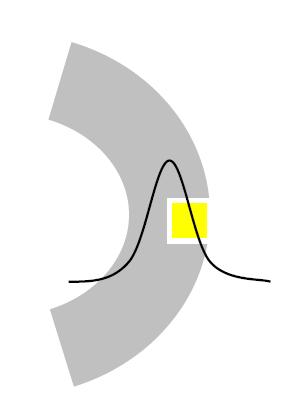
4 In the conventional approach to study the splitting modes using microspheres, because the interaction between the fiber tip (or nanoparticle) and the evanescent mode of the microsphere is very small, it leads to a very small change in the effective refractive index of the sphere, which shifts the wavelength position of the peaks and causes small splitting in the resonator transmission (or reflection) spectrum, these changes are typically on the order of pm in size 12. In order to detect such small shifts, one must normally use an expensive tunable narrow-linewidth laser source to scan the relevant spectral region of the resonator output spectrum. Furthermore, the resonator itself must be designed to yield a very narrow linewidth, so that the small peak shifts and splitting can be detected. This requires a high finesse (free spectral range divided by linewidth), or equivalently high quality factor (operating wavelength divided by linewidth ~ 10 8 ), which translates to low loss waveguides in the resonator and weak coupling between the resonator and fiber tip. Here we demonstrated strong coupling between on chip notched ring resonator and nanoparticle, where the nanoparticle can be placed inside the notch. Compared to the ring resonator without notch, as illustrated in Fig.1b, where the interaction strength between the nanoparticle and the resonator mode field is relatively weak and only a small portion of the field (evanescent tail) is interacting with the nanoparticle, the notch provides access to the peak of the electromagnetic field localized in the core, so that when a nanoparticle is placed there, the strong core field, rather than the weak evanescent cladding field, overlaps the nanoparticle and thereby produces an enhanced response, as shown in Fig.1c. The on-chip photonic device configuration of a micro resonator with a notch, nanoparticle and integrated with two bus waveguide has been fabricated The notch of 100nm size in the ring was fabricated by e-beam lithography. We have analyzed the case of a 100nm long notch with a 4
5 20nm diameter dielectric nano particle Si tip and 20nm diameter metallic Au particle inside the notch. The thickness of Si waveguide is 220nm. Fig. 2a is the image of the 100nm sized notch in the micro resonator using portable SEM (Hitachi TM-1000). The ring resonator is 4.0µm in diameter with the waveguide width of 200nm. The core material of the ring is Si with refractive index 3.48 at around 1.53µm wavelength, and the bottom cladding material is SiO 2 with refractive index We used SOI wafer for the small ring resonator fabrication, and an e-beam is utilized to fabricate the 100nmx100nm notch size at the edge of the Si micro ring resonator. The refractive index of the Au nanoparticle tip is i at 1.53µm. Fig.2b is the SEM image within the coupling gap area, which shows the clear 100nm gap between the bus waveguide and the notched ring resonator. A tunable laser from 1480nm to 1580nm is used to couple the light from tapered optical fiber to the Si waveguide, a Ge detector is put at other end to collect the through port signal. Fig.3 is the measurement result for the Through port of bus waveguide for the ring resonator with notch at the edge. We can clearly see the splitting of the original resonance modes at around 1.53µm, which represents the bonding photonic mode at shorter wavelength (1.534 µm) and the anti bonding photonic mode at longer wavelength (1.537 µm). The splitting width is almost 3nm; this nm scale splitting bandwidth is much larger than the pm splitting bandwidth we normally see for the fiber tip close to the microsphere resonator. We used a Si nanoparticle tip with 20nm in diameter and put it inside the center of 100nm size notch of the ring resonator using portable AFM, transmission at Through port of the coupled waveguide is shown at Fig.4a. It is observed that the bonding mode is red shifted by 1.1nm, while the position of the anti bonding mode is almost unchanged, leading to a smaller splitting bandwidth due to the red shift of the bonding mode. Next the Si nanoparticle tip is replaced with 5
6 a 20nm Au nanoparticle tip and also put inside the notch center of the micro ring resonator. We see the dramatically different shift with the Au nanoparticle for the bonding state, a 1nm blue shift is observed instead and the anti bonding state remains unchanged, causing larger splitting bandwidth than the original splitting due to the notch with just air, as shown in Fig.4b. The results reveal the drastically different photonic mode properties between the symmetric and anti symmetric states and suggests that we can utilize the nanoparticle to study the photonic molecule characteristics. We can understand the red shift induced by the Si nanoparticle by considering an effective index increase in the notch due to the substitution of air with high index Si; the same reason for Au nanoparticle, as the real part is less than that of Air. We can also understand the fact that nanoparticles have little effect on the anti-bonding mode by considering that they are placed at the center of the notch and close to the zero field node of the anti-bonding mode. It can be clearly seen that the strong coupling effect of a nanoparticle placed in a notch is fundamentally different from the evanescent coupling effect of a nanoparticle placed in the evanescent field of the resonator, which high Q microspheres are often used. The different wavelength shift between a dielectric Si nanoparticle and a metallic Au nanoparticle, as well as the splitting bandwidth narrowing with the dielectric Si compared to the widening with the metallic Au nanoparticle, provides us with a unique, self referencing mechanism to distinguish these different types of nanoparticles. This is very important for the bio sensor area utilizing nanoparticles, as Au nanoparticles are often used for tagging, but other dielectric nanoparticles other than the analyte may be present and cause misleading sensing signals, Au nanoparticle s unique effects on the shift direction and the splitting bandwidth widening will enable us to distinguish the real signal from the background dielectric nanoparticle 6
7 noise and greatly enhance the signal to noise ratio. The intentionally fabricated notch in the micro ring resonator provides us with a localized position to trap the nanoparticle. Based on the strong splitting and wavelength shift when the nanoparticle is localized in the notch, we can identify whether the nanoparticle stays within the fabricated notch and differentiate the nanoparticle position. The future study on the electromagnetic force applied upon the nanoparticle close to the notch will be interesting to help us to understand the mechanic response from the notch and how to deliver the nanoparticle to the notch. In summary, we have experimentally demonstrated the strong coupling between on chip nanoscale notched ring resonators and nanoparticle, in which a notch is introduced in the resonator to provide access to the core field, which is drastically different from previous studies using evanescent coupling to microsphere. Placing a nanoparticle in the notch produces a much stronger response than simply placing the nanoparticle in contact with the exterior of the core. In the exemplary case of a dielectric silicon and metallic gold nanoparticle placed in a notch, we have demonstrated that nanoparticle induces a large wavelength splitting (~nm) and very different shift in the resonant modes of the resonator. This is a significant improvement over the smaller wavelength shifts and splitting (~pm) observed in earlier experiments where the particle was placed outside the core of a conventional microsphere resonator, and lowers the requirement for very high Q resonator devices. Note that the utility of this approach is not limited to ring resonators used as examples here, but can be extended to other types of resonator geometries, such as racetracks, and polygons. This work provides us a unique way to achieve single nanoparticle detection and sorting with thousands of times signal enhancement. The nature of the on chip microresonators will also make large scale integration on a sing chip possible. 7
8 We thank the support from Microsystems Technology Laboratory and Center for Materials Science and Engineering at MIT for the access to the facility and measurement equipments, High Performance Computing center at CUNY, and 3M central research lab. References 1. W. D. Li, S. Y. Chou, Opt. Exp. 18, 931 (2010) 2. B. E. Little, S. T. Chu, and H. A. Haus, Opt. Lett., 23, 1570 (1998) 3. S. V. Boriskina, J. Opt. Soc. Am. B, 23, 1565 (2006) 4. A. Yariv, Y. Xu, R. K. Lee, and A. Scherer, Opt. Lett. 24, (1999) 5. Q. Song, H. Cao, S. T. Ho, and G. S. Solomon, Appl. Phys. Lett., 94, (2009) 6. A. Francois and M. Himmelhausa, Appl. Phys. Lett., 92, (2008) 7. M. L. Gorodetsky, A. D. Pryamikov, and V. S. Ilchenko, J. Opt. Soc. Am. B, 17, 1051 (2000) 8. Z. Yuan, B. E. Kardynal, R. M. Stevenson, A. J. Shields, C. J. Lobo, K. Cooper, N. S. Beattie, D. A. Ritchie, and M. Pepper, Science, 295, 102 (2002) 9. M. Bruchez, M. Moronne, P. Gin, S. Weiss, and A. Paul Alivisatos, Science, 281, 2013 (1998) 10. C. Loo, A. Lin, L. Hirsch, M. Lee, J. Barton, N. Halas, J. West, R. Drezek, Technol. Cancer Res. Treat., 3, 33 (2004) 11. R. Wiese, Luminescence, 18, 25 (2003) 12. A. Mazzei, S. Gotzinger, L. de S. Menezes, G. Zumofen, O. Benson,1, and V. Sandoghdar, Phys. Rev. Lett., 99, (2007) 13. M. Borselli, T. J. Johnson, and O. Painter, Opt. Exp., 13, 1515 (2005) 14. A. Gondarenko, J. S. Levy, and M. Lipson, Opt. Exp. 17, (2009) 8
9 15. E. S. Hosseini, S. Yegnanarayanan, A. H. Atabaki, M. Soltani, and A. Adibi, Opt. Exp., 17, (2009) 16. B. Koch, Y. Yi, J. Zhang, S. Znameroski, and T. Smith, Appl. Phys. Lett., 95, (2009) 17. T. Barwicz, M. A. Popovic, P. T. Rakich, M. R. Watts, H. A. Haus, E. P. Ippen, and H. I. Smith, Opt. Exp., 12, 1437 (2004) 9
10 Figure captions: Figure 1 (a) The notched micro ring resonator and the coupling to the bus waveguide with input and output ports. The bus and ring waveguide width is 200nm. The notch size is around 100nmx100nm. (b) The evanescent coupling between the resonance mode and the nanoparticle. (c) The notch in the microring resonator. The nanoparticle is in the notch and coupling to the core of the resonance mode, the black curve represents the single mode behavior for the ring waveguide. The ring waveguide is a sing mode waveguide at 1.53µm. Figure 2 (a) The image of the 100nm size notch by portable SEM. (b) The SEM image with clear 100nm coupling gap between the notched ring resonator and the single mode bus waveguide. Figure 3 The transmission at Through port around 1.53µm, the splitting is around 3nm, the bonding photonic mode is at shorter wavelength µm and anti bonding photonic mode is at longer wavelength µm. Figure 4 (a) Si nanoparticle tip with 20nm in diameter is put inside the 100nm notch size of the ring resonator, the Through port from the coupled waveguide is shown, it is observed that the bonding mode wavelength (resonance at shorter wavelength) is red shifted with 1.1nm, while the wavelength of the anti bonding mode (resonance at longer wavelength) is almost unchanged, the splitting bandwidth is smaller due to the red shift of the bonding mode. (b) 20nm Au nanoparticle tip is put inside the notch size of the micro ring resonator, we see the dramatic different shift from the Au nanoparticle for the bonding state (resonance at shorter wavelength), the 1.0nm blue shift is observed instead and the anti bonding state (resonance at longer wavelength) is still unchanged, the splitting bandwidth is larger than the original splitting due to the notch with air. 10

 (b)")
11 Input port Through port (a) (b) (c) 11
")
12 100nm 200nm (a) (b) 12
13 13
14 (a) (b) 14
Metallic nanoparticle on micro ring resonator for bio optical detection and sensing
 Metallic nanoparticle on micro ring resonator for bio optical detection and sensing Ali Haddadpour 1,3 2, 3, 4, * and Yasha Yi 1 Faculty of Electrical and Computer Engineering, University of Tabriz, Tabriz,
Light Interaction with Small Structures
 Light Interaction with Small Structures Molecules Light scattering due to harmonically driven dipole oscillator Nanoparticles Insulators Rayleigh Scattering (blue sky) Semiconductors...Resonance absorption
Sensing: a unified perspective for integrated photonics
 Sensing: a unified perspective for integrated photonics Chemical detection Environmental monitoring Process control Warfighter protection Biological sensing Drug discovery Food safety Medical diagnosis
PROCEEDINGS OF SPIE. Nanoparticle sorting in silicon waveguide arrays. H. T. Zhao, Y. Zhang, L. K. Chin, P. H. Yap, K. Wang, et al.
 PROCEEDINGS OF SPIE SPIEDigitalLibrary.org/conference-proceedings-of-spie Nanoparticle sorting in silicon waveguide arrays H. T. Zhao, Y. Zhang, L. K. Chin, P. H. Yap, K. Wang, et al. H. T. Zhao, Y. Zhang,
Photonic Crystal Nanocavities for Efficient Light Confinement and Emission
 Journal of the Korean Physical Society, Vol. 42, No., February 2003, pp. 768 773 Photonic Crystal Nanocavities for Efficient Light Confinement and Emission Axel Scherer, T. Yoshie, M. Lončar, J. Vučković
Ultra-Slow Light Propagation in Room Temperature Solids. Robert W. Boyd
 Ultra-Slow Light Propagation in Room Temperature Solids Robert W. Boyd The Institute of Optics and Department of Physics and Astronomy University of Rochester, Rochester, NY USA http://www.optics.rochester.edu
SUPPLEMENTAL MATERIAL I: SEM IMAGE OF PHOTONIC CRYSTAL RESONATOR
 1 SUPPLEMENTAL MATERIAL I: SEM IMAGE OF PHOTONIC CRYSTAL RESONATOR Figure S1 below is a scanning electronic microscopy image of a typical evanescently coupled photonic crystal resonator used in these experiments.
ECE 484 Semiconductor Lasers
 ECE 484 Semiconductor Lasers Dr. Lukas Chrostowski Department of Electrical and Computer Engineering University of British Columbia January, 2013 Module Learning Objectives: Understand the importance of
Seminars in Nanosystems - I
 Seminars in Nanosystems - I Winter Semester 2011/2012 Dr. Emanuela Margapoti Emanuela.Margapoti@wsi.tum.de Dr. Gregor Koblmüller Gregor.Koblmueller@wsi.tum.de Seminar Room at ZNN 1 floor Topics of the
There s plenty of room at the bottom! - R.P. Feynman, Nanostructure: a piece of material with at least one dimension less than 100 nm in extent.
 Nanostructures and Nanotechnology There s plenty of room at the bottom! - R.P. Feynman, 1959 Materials behave differently when structured at the nm scale than they do in bulk. Technologies now exist that
ESH Benign Processes for he Integration of Quantum Dots (QDs)
") ESH Benign Processes for he Integration of Quantum Dots (QDs) PIs: Karen K. Gleason, Department of Chemical Engineering, MIT Graduate Students: Chia-Hua Lee: PhD Candidate, Department of Material Science
ESH Benign Processes for he Integration of Quantum Dots (QDs) PIs: Karen K. Gleason, Department of Chemical Engineering, MIT Graduate Students: Chia-Hua Lee: PhD Candidate, Department of Material Science
Fabrication-tolerant high quality factor photonic crystal microcavities
 Fabrication-tolerant high quality factor photonic crystal microcavities Kartik Srinivasan, Paul E. Barclay, and Oskar Painter Department of Applied Physics, California Institute of Technology, Pasadena,
Polarization control and sensing with two-dimensional coupled photonic crystal microcavity arrays. Hatice Altug * and Jelena Vučković
 Polarization control and sensing with two-dimensional coupled photonic crystal microcavity arrays Hatice Altug * and Jelena Vučković Edward L. Ginzton Laboratory, Stanford University, Stanford, CA 94305-4088
Enhancement mechanisms for optical forces in integrated optics
 Enhancement mechanisms for optical forces in integrated optics M. L. Povinelli (a),m.lončar (b),e.j.smythe (b),m.ibanescu (c), S. G. Johnson (d), F. Capasso (b), and J. D. Joannopoulos (c) (a) Ginzton
Photonic crystal with multiple-hole defect for sensor applications
 Photonic crystal with multiple-hole defect for sensor applications Christopher Kang 1,* and Sharon M. Weiss 1,2 1 Interdisciplinary Graduate Program in Materials Science, Vanderbilt University, Nashville,
Nanophotonics: solar and thermal applications
 Nanophotonics: solar and thermal applications Shanhui Fan Ginzton Laboratory and Department of Electrical Engineering Stanford University http://www.stanford.edu/~shanhui Nanophotonic Structures Photonic
Negative curvature fibers
 Negative curvature fibers presented by Jonathan Hu 1 with Chengli Wei, 1 R. Joseph Weiblen, 2,* and Curtis R. Menyuk 2 1 Baylor University, Waco, Texas 76798, USA 2 University of Maryland Baltimore County,
Advanced techniques Local probes, SNOM
 Advanced techniques Local probes, SNOM Principle Probe the near field electromagnetic field with a local probe near field probe propagating field evanescent Advanced techniques Local probes, SNOM Principle
arxiv: v1 [physics.bio-ph] 11 Sep 2015
![arxiv: v1 [physics.bio-ph] 11 Sep 2015](/thumbs/87/97055193.jpg "arxiv: v1 [physics.bio-ph] 11 Sep 2015") arxiv:1509.04625v1 [physics.bio-ph] 11 Sep 2015 IR-Laser Welding and Ablation of Biotissue Stained with Metal Nanoparticles A. A. Lalayan, S. S. Israelyan Centre of Strong Fields Physics, Yerevan State
arxiv:1509.04625v1 [physics.bio-ph] 11 Sep 2015 IR-Laser Welding and Ablation of Biotissue Stained with Metal Nanoparticles A. A. Lalayan, S. S. Israelyan Centre of Strong Fields Physics, Yerevan State
Nanophysics: Main trends
 Nano-opto-electronics Nanophysics: Main trends Nanomechanics Main issues Light interaction with small structures Molecules Nanoparticles (semiconductor and metallic) Microparticles Photonic crystals Nanoplasmonics
Morphology-dependent resonance induced by two-photon excitation in a micro-sphere trapped by a femtosecond pulsed laser
 Morphology-dependent resonance induced by two-photon excitation in a micro-sphere trapped by a femtosecond pulsed laser Dru Morrish, Xiaosong Gan and Min Gu Centre for Micro-Photonics, School of Biophysical
Energy transport in metal nanoparticle plasmon waveguides
 Energy transport in metal nanoparticle plasmon waveguides Stefan A. Maier, Pieter G. Kik, and Harry A. Atwater California Institute of Technology Thomas J. Watson Laboratory of Applied Physics, Pasadena,
Surface plasmon waveguides
 Surface plasmon waveguides Introduction Size Mismatch between Scaled CMOS Electronics and Planar Photonics Photonic integrated system with subwavelength scale components CMOS transistor: Medium-sized molecule
Self-assembled nanostructures for antireflection optical coatings
 Self-assembled nanostructures for antireflection optical coatings Yang Zhao 1, Guangzhao Mao 2, and Jinsong Wang 1 1. Deaprtment of Electrical and Computer Engineering 2. Departmentof Chemical Engineering
Two-photon single-beam particle trapping of active micro-spheres
 Two-photon single-beam particle trapping of active micro-spheres Dru Morrish, Xiaosong Gan and Min Gu * Centre for Mirco-Photonics, School of Biophysical Sciences and Electrical Engineering, Swinburne
Towards the Lasing Spaser: Controlling. Metamaterial Optical Response with Semiconductor. Quantum Dots
 Towards the Lasing Spaser: Controlling Metamaterial Optical Response with Semiconductor Quantum Dots E. Plum, V. A. Fedotov, P. Kuo, D. P. Tsai, and N. I. Zheludev,, Optoelectronics Research Centre, University
Nanocomposite photonic crystal devices
 Nanocomposite photonic crystal devices Xiaoyong Hu, Cuicui Lu, Yulan Fu, Yu Zhu, Yingbo Zhang, Hong Yang, Qihuang Gong Department of Physics, Peking University, Beijing, P. R. China Contents Motivation
29: Nanotechnology. What is Nanotechnology? Properties Control and Understanding. Nanomaterials
 29: Nanotechnology What is Nanotechnology? Properties Control and Understanding Nanomaterials Making nanomaterials Seeing at the nanoscale Quantum Dots Carbon Nanotubes Biology at the Nanoscale Some Applications
Single Semiconductor Nanostructures for Quantum Photonics Applications: A solid-state cavity-qed system with semiconductor quantum dots
 The 3 rd GCOE Symposium 2/17-19, 19, 2011 Tohoku University, Sendai, Japan Single Semiconductor Nanostructures for Quantum Photonics Applications: A solid-state cavity-qed system with semiconductor quantum
Nanoscale optical circuits: controlling light using localized surface plasmon resonances
 Nanoscale optical circuits: controlling light using localized surface plasmon resonances T. J. Davis, D. E. Gómez and K. C. Vernon CSIRO Materials Science and Engineering Localized surface plasmon (LSP)
Optics and Spectroscopy
 Introduction to Optics and Spectroscopy beyond the diffraction limit Chi Chen 陳祺 Research Center for Applied Science, Academia Sinica 2015Apr09 1 Light and Optics 2 Light as Wave Application 3 Electromagnetic
Enhancing the Rate of Spontaneous Emission in Active Core-Shell Nanowire Resonators
 Chapter 6 Enhancing the Rate of Spontaneous Emission in Active Core-Shell Nanowire Resonators 6.1 Introduction Researchers have devoted considerable effort to enhancing light emission from semiconductors
Optics of complex micro structures
 Optics of complex micro structures dielectric materials λ L disordered partially ordered ordered random multiple scattering liquid crystals quasi crystals (Fibonacci) photonic crystals Assembly of photonic
A microring multimode laser using hollow polymer optical fibre
 PRAMANA c Indian Academy of Sciences Vol. 75, No. 5 journal of November 2010 physics pp. 923 927 A microring multimode laser using hollow polymer optical fibre M KAILASNATH, V P N NAMPOORI and P RADHAKRISHNAN
Optimizing the performance of metal-semiconductor-metal photodetectors by embedding nanoparticles in the absorption layer
 Journal of Electrical and Electronic Engineering 2015; 3(2-1): 78-82 Published online February 10, 2015 (http://www.sciencepublishinggroup.com/j/jeee) doi: 10.11648/j.jeee.s.2015030201.27 ISSN: 2329-1613
The Dielectric Function of a Metal ( Jellium )
") The Dielectric Function of a Metal ( Jellium ) Total reflection Plasma frequency p (10 15 Hz range) Why are Metals Shiny? An electric field cannot exist inside a metal, because metal electrons follow the
The Dielectric Function of a Metal ( Jellium ) Total reflection Plasma frequency p (10 15 Hz range) Why are Metals Shiny? An electric field cannot exist inside a metal, because metal electrons follow the
Since the pioneering work of Ritchie in 1957, there has
 pubs.acs.org/nanolett A Surface Plasmon Enhanced Infrared Photodetector Based on InAs Quantum Dots Chun-Chieh Chang, Yagya D. Sharma, Yong-Sung Kim, Jim A. Bur, Rajeev V. Shenoi, Sanjay Krishna, Danhong
Nanomaterials and their Optical Applications
 Nanomaterials and their Optical Applications Winter Semester 2013 Lecture 02 rachel.grange@uni-jena.de http://www.iap.uni-jena.de/multiphoton Lecture 2: outline 2 Introduction to Nanophotonics Theoretical
Investigation on Mode Splitting and Degeneracy in the L3 Photonic Crystal Nanocavity via Unsymmetrical Displacement of Air-Holes
 The International Journal Of Engineering And Science (Ijes) Volume 2 Issue 2 Pages 146-150 2013 Issn: 2319 1813 Isbn: 2319 1805 Investigation on Mode Splitting and Degeneracy in the L3 Photonic Crystal
The National Nanotechnology Initiative
 The National Nanotechnology Initiative and Nano-scale Length Metrology T.V. Vorburger (tvtv@nist.gov), Precision Engineering Division R.G. Dixson, J. Fu, N.G. Orji, M.W. Cresswell, R.A. Allen, W.F. Guthrie,
Multi-cycle THz pulse generation in poled lithium niobate crystals
 Laser Focus World April 2005 issue (pp. 67-72). Multi-cycle THz pulse generation in poled lithium niobate crystals Yun-Shik Lee and Theodore B. Norris Yun-Shik Lee is an assistant professor of physics
Time Domain Modeling of All-Optical Switch based on PT-Symmetric Bragg Grating
 Time Domain Modeling of All-Optical Switch based on PT-Symmetric Bragg Grating Sendy Phang 1, Ana Vukovic 1, Hadi Susanto 2, Trevor M. Benson 1, and Phillip Sewell 1 1 School of Electrical and Electronic
Resonator Fabrication for Cavity Enhanced, Tunable Si/Ge Quantum Cascade Detectors
 Resonator Fabrication for Cavity Enhanced, Tunable Si/Ge Quantum Cascade Detectors M. Grydlik 1, P. Rauter 1, T. Fromherz 1, G. Bauer 1, L. Diehl 2, C. Falub 2, G. Dehlinger 2, H. Sigg 2, D. Grützmacher
Quantum Technologies CCEM Workshop March 23 rd, 2017
 Quantum Technologies CCEM Workshop March 23 rd, 2017 JT Janssen Welcome to the National Physical Laboratory The first quantum revolution h V n f 2 e 1 The second quantum revolution Superposition Entanglement
PLASMONICS/METAMATERIALS
 PLASMONICS/METAMATERIALS Interconnects Optical processing of data Subwavelength confinement Electrodes are in place Coupling to other on-chip devices Combination of guiding, detection, modulation, sensing
Nanoscale confinement of photon and electron
 Nanoscale confinement of photon and electron Photons can be confined via: Planar waveguides or microcavities (2 d) Optical fibers (1 d) Micro/nano spheres (0 d) Electrons can be confined via: Quantum well
Nanotechnology. Gavin Lawes Department of Physics and Astronomy
 Nanotechnology Gavin Lawes Department of Physics and Astronomy Earth-Moon distance 4x10 8 m (courtesy NASA) Length scales (Part I) Person 2m Magnetic nanoparticle 5x10⁻⁹ m 10 10 m 10 5 m 1 m 10-5 m 10-10
Photonics Beyond Diffraction Limit:
 Photonics Beyond Diffraction Limit: Plasmon Cavity, Waveguide and Lasers Xiang Zhang University of California, Berkeley Light-Matter Interaction: Electrons and Photons Photons Visible / IR ~ 1 m Electrons
Terahertz sensing and imaging based on carbon nanotubes:
 Terahertz sensing and imaging based on carbon nanotubes: Frequency-selective detection and near-field imaging Yukio Kawano RIKEN, JST PRESTO ykawano@riken.jp http://www.riken.jp/lab-www/adv_device/kawano/index.html
Temperature Dependence of a Macrobending Edge Filter Based on a High-bend Loss Fiber
 Dublin Institute of Technology ARROW@DIT Articles School of Electrical and Electronic Engineering 2007-12-31 Temperature Dependence of a Macrobending Edge Filter Based on a High-bend Loss Fiber Pengfei
NANOCOMPOSITE THIN FILMS:
 NANOCOMPOSITE THIN FILMS: Assembly, Characterizations, & Applications Chaoyang Jiang Department of Chemistry The University of South Dakota St. Louis, June 26, 2008 Forest Products &Nanocomposite P. Monteiro@UC
2008,, Jan 7 All-Paid US-Japan Winter School on New Functionalities in Glass. Controlling Light with Nonlinear Optical Glasses and Plasmonic Glasses
 2008,, Jan 7 All-Paid US-Japan Winter School on New Functionalities in Glass Photonic Glass Controlling Light with Nonlinear Optical Glasses and Plasmonic Glasses Takumi FUJIWARA Tohoku University Department
Quantum Dot Lasers. Jose Mayen ECE 355
 Quantum Dot Lasers Jose Mayen ECE 355 Overview of Presentation Quantum Dots Operation Principles Fabrication of Q-dot lasers Advantages over other lasers Characteristics of Q-dot laser Types of Q-dot lasers
Magnetic and optic sensing. Magnetic sensors
 Magnetic and optic sensing Magnetic sensors 1 Literature Physics of Semiconductor Devices S.M. Sze, Kwok K. Ng Available as ebook on http://www.lub.lu.se/en/search/lubsearch.ht ml This lecture chapters
ORGANIC MOLECULES in photonics
 ORGANIC MOLECULES in photonics Progress in Photonics, Florence 16.10. 2015 probe surface scattered waves Costanza Toninelli www.lens.unifi.it/quantum- nanophotonics Single Molecules: From Sensing To Quantum
Natallia Strekal. Plasmonic films of noble metals for nanophotonics
 Natallia Strekal Plasmonic films of noble metals for nanophotonics The aim of our investigation is the mechanisms of light interactions with nanostructure and High Tech application in the field of nanophotonics
Einführung in die Photonik II
 Einführung in die Photonik II ab 16.April 2012, Mo 11:00-12:30 Uhr SR 218 Lectures Monday, 11:00 Uhr, room 224 Frank Cichos Molecular Nanophotonics Room 322 Tel.: 97 32571 cichos@physik.uni-leipzig.de
Photonic nanojet enhancement of backscattering of light by nanoparticles: a potential novel visible-light ultramicroscopy technique
 Photonic nanojet enhancement of backscattering of light by nanoparticles: a potential novel visible-light ultramicroscopy technique Zhigang Chen and Allen Taflove Department of Electrical and Computer
Quantum Photonic Integrated Circuits
 Quantum Photonic Integrated Circuits IHFG Hauptseminar: Nanooptik und Nanophotonik Supervisor: Prof. Dr. Peter Michler 14.07.2016 Motivation and Contents 1 Quantum Computer Basics and Materials Photon
Two-dimensional porous silicon photonic crystal light emitters
 Two-dimensional porous silicon photonic crystal light emitters Maria Makarova, Jelena Vuckovic, Hiroyuki Sanda, Yoshio Nishi Department of Electrical Engineering, Stanford University, Stanford, CA 94305-4088
Photonic crystals. Semi-conductor crystals for light. The smallest dielectric lossless structures to control whereto and how fast light flows
 Photonic crystals Semi-conductor crystals for light The smallest dielectric lossless structures to control whereto and how fast light flows Femius Koenderink Center for Nanophotonics AMOLF, Amsterdam f.koenderink@amolf.nl
Backscattering enhancement of light by nanoparticles positioned in localized optical intensity peaks
 Backscattering enhancement of light by nanoparticles positioned in localized optical intensity peaks Zhigang Chen, Xu Li, Allen Taflove, and Vadim Backman We report what we believe to be a novel backscattering
Optimum Access Waveguide Width for 1xN Multimode. Interference Couplers on Silicon Nanomembrane
 Optimum Access Waveguide Width for 1xN Multimode Interference Couplers on Silicon Nanomembrane Amir Hosseini 1,*, Harish Subbaraman 2, David Kwong 1, Yang Zhang 1, and Ray T. Chen 1,* 1 Microelectronic
U-Shaped Nano-Apertures for Enhanced Optical Transmission and Resolution
 U-Shaped Nano-Apertures for Enhanced Optical Transmission and Resolution Mustafa Turkmen 1,2,3, Serap Aksu 3,4, A. Engin Çetin 2,3, Ahmet A. Yanik 2,3, Alp Artar 2,3, Hatice Altug 2,3,4, * 1 Electrical
Title. Author(s)Nagasaki, Akira; Saitoh, Kunimasa; Koshiba, Masanori. CitationOptics Express, 19(4): Issue Date Doc URL.
Nagasaki, Akira; Saitoh, Kunimasa; Koshiba, Masanori. CitationOptics Express, 19(4): Issue Date Doc URL.") Title Polarization characteristics of photonic crystal fib Author(s)Nagasaki, Akira; Saitoh, Kunimasa; Koshiba, Masanori CitationOptics Express, 19(4): 3799-3808 Issue Date 2011-02-14 Doc URL http://hdl.handle.net/2115/45257
Title Polarization characteristics of photonic crystal fib Author(s)Nagasaki, Akira; Saitoh, Kunimasa; Koshiba, Masanori CitationOptics Express, 19(4): 3799-3808 Issue Date 2011-02-14 Doc URL http://hdl.handle.net/2115/45257
PANDA ring resonator for optical Gas and Pressure sensing applications
 I J C T A, 9(8), 016, pp. 3415-34 International Science Press PANDA ring resonator for optical Gas and Pressure sensing applications G. Bhuvaneswari*, D. Shanmuga sundar* and A. Sivanantha Raja* ABSTRACT
Acoustic metamaterials in nanoscale
 Acoustic metamaterials in nanoscale Dr. Ari Salmi www.helsinki.fi/yliopisto 12.2.2014 1 Revisit to resonances Matemaattis-luonnontieteellinen tiedekunta / Henkilön nimi / Esityksen nimi www.helsinki.fi/yliopisto
Alexander Gaeta Department of Applied Physics and Applied Mathematics Michal Lipson Department of Electrical Engineering
 Chip-Based Optical Frequency Combs Alexander Gaeta Department of Applied Physics and Applied Mathematics Michal Lipson Department of Electrical Engineering KISS Frequency Comb Workshop Cal Tech, Nov. 2-5,
Ultracompact and silicon-on-insulator-compatible polarization splitter based on asymmetric plasmonic dielectric coupling
 Appl. Phys. B DOI 10.1007/s00340-013-5457-7 Ultracompact and silicon-on-insulator-compatible polarization splitter based on asymmetric plasmonic dielectric coupling Linfei Gao Feifei Hu Xingjun Wang Liangxiao
RECENT innovations in nanoscale optical technologies
 478 IEEE JOURNAL OF SELECTED TOPICS IN QUANTUM ELECTRONICS, VOL. 10, NO. 3, MAY/JUNE 2004 Tunable Optical Nanocavity Based on Modulation of Near-Field Coupling Between Subwavelength Periodic Nanostructures
SUPPLEMENTARY INFORMATION
 SUPPLEMENTARY INFORMATION Supplementary Information I. Schematic representation of the zero- n superlattices Schematic representation of a superlattice with 3 superperiods is shown in Fig. S1. The superlattice
Design of a Multi-Mode Interference Crossing Structure for Three Periodic Dielectric Waveguides
 Progress In Electromagnetics Research Letters, Vol. 75, 47 52, 2018 Design of a Multi-Mode Interference Crossing Structure for Three Periodic Dielectric Waveguides Haibin Chen 1, Zhongjiao He 2,andWeiWang
Vertically Emitting Microdisk Lasers
 Excerpt from the Proceedings of the COMSOL Conference 008 Hannover Vertically Emitting Microdisk Lasers Lukas Mahler *,1, Alessandro Tredicucci 1 and Fabio Beltram 1 1 NEST-INFM and Scuola Normale Superiore,
Fundamentals of nanoscience
 Fundamentals of nanoscience Spectroscopy of nano-objects Mika Pettersson 1. Non-spatially resolved spectroscopy Traditionally, in spectroscopy, one is interested in obtaining information on the energy
Near-Field Nano/Atom Optics and Technology
 M. Ohtsu (Ed.) Near-Field Nano/Atom Optics and Technology With 189 Figures / Springer Preface List of Contributors V VII XIII 1. Introduction 1 1.1 Near-Field Optics and Related Technologies 1 1.2 History
Progress In Electromagnetics Research, PIER 77, , 2007
 Progress In Electromagnetics Research, PIER 77, 49 7, 7 A NOVEL PROPOSAL FOR ULTRA-HIGH RESOLUTION AND COMPACT OPTICAL DISPLACEMENT SENSOR BASED ON ELECTROMAGNETICALLY INDUCED TRANSPARENCY IN RING RESONATOR
Large-Area and Uniform Surface-Enhanced Raman. Saturation
 Supporting Information Large-Area and Uniform Surface-Enhanced Raman Spectroscopy Substrate Optimized by Enhancement Saturation Daejong Yang 1, Hyunjun Cho 2, Sukmo Koo 1, Sagar R. Vaidyanathan 2, Kelly
Surface-Plasmon Sensors
 Surface-Plasmon Sensors Seok Ho Song Physics Department in Hanyang University Dongho Shin, Jaewoong Yun, Kihyong Choi Gwansu Lee, Samsung Electro-Mechanics Contents Dispersion relation of surface plasmons
MINIMIZING REFLECTION AND FOCUSSING OF INCIDENT WAVE TO ENHANCE ENERGY DEPOSITION IN PHOTODETECTOR S ACTIVE REGION
 Progress In Electromagnetics Research, PIER 65, 71 80, 2006 MINIMIZING REFLECTION AND FOCUSSING OF INCIDENT WAVE TO ENHANCE ENERGY DEPOSITION IN PHOTODETECTOR S ACTIVE REGION A. A. Pavel, P. Kirawanich,
Ge Quantum Well Modulators on Si. D. A. B. Miller, R. K. Schaevitz, J. E. Roth, Shen Ren, and Onur Fidaner
 10.1149/1.2986844 The Electrochemical Society Ge Quantum Well Modulators on Si D. A. B. Miller, R. K. Schaevitz, J. E. Roth, Shen Ren, and Onur Fidaner Ginzton Laboratory, 450 Via Palou, Stanford CA 94305-4088,
Supplemental Information for
 Supplemental Information for Densely arranged two-dimensional silver nanoparticle assemblies with optical uniformity over vast areas as excellent surface-enhanced Raman scattering substrates Yoshimasa
Investigating functionalized active coated nanoparticles for use in nano-sensing applications
 Investigating functionalized active coated nanoparticles for use in nano-sensing applications Joshua A. Gordon 1*, Richard W. Ziolkowski 2, 1 1 College of Optical Sciences, University of Arizona, Tucson,
Simulations of nanophotonic waveguides and devices using COMSOL Multiphysics
 Presented at the COMSOL Conference 2010 China Simulations of nanophotonic waveguides and devices using COMSOL Multiphysics Zheng Zheng Beihang University 37 Xueyuan Road, Beijing 100191, China Acknowledgement
ME 4875/MTE C16. Introduction to Nanomaterials and Nanotechnology. Lecture 2 - Applications of Nanomaterials + Projects
 ME 4875/MTE 575 - C16 Introduction to Nanomaterials and Nanotechnology Lecture 2 - Applications of Nanomaterials + Projects 1 Project Teams of 4 students each Literature review of one application of nanotechnology
Single Emitter Detection with Fluorescence and Extinction Spectroscopy
 Single Emitter Detection with Fluorescence and Extinction Spectroscopy Michael Krall Elements of Nanophotonics Associated Seminar Recent Progress in Nanooptics & Photonics May 07, 2009 Outline Single molecule
Plasmonics. The long wavelength of light ( μm) creates a problem for extending optoelectronics into the nanometer regime.
 creates a problem for extending optoelectronics into the nanometer regime.") Plasmonics The long wavelength of light ( μm) creates a problem for extending optoelectronics into the nanometer regime. A possible way out is the conversion of light into plasmons. They have much shorter
Plasmonics The long wavelength of light ( μm) creates a problem for extending optoelectronics into the nanometer regime. A possible way out is the conversion of light into plasmons. They have much shorter
In the name of Allah
 In the name of Allah Nano chemistry- 4 th stage Lecture No. 1 History of nanotechnology 16-10-2016 Assistance prof. Dr. Luma Majeed Ahmed lumamajeed2013@gmail.com, luma.ahmed@uokerbala.edu.iq Nano chemistry-4
A normal-incident quantum well infrared photodetector enhanced by surface plasmon resonance
 Best Student Paper Award A normal-incident quantum well infrared photodetector enhanced by surface plasmon resonance Wei Wu a, Alireza Bonakdar, Ryan Gelfand, and Hooman Mohseni Bio-inspired Sensors and
Quantum Dots for Advanced Research and Devices
 Quantum Dots for Advanced Research and Devices spectral region from 450 to 630 nm Zero-D Perovskite Emit light at 520 nm ABOUT QUANTUM SOLUTIONS QUANTUM SOLUTIONS company is an expert in the synthesis
Polarization control of defect modes in threedimensional woodpile photonic crystals
 Polarization control of defect modes in threedimensional woodpile photonic crystals Michael James Ventura and Min Gu* Centre for Micro-Photonics and Centre for Ultrahigh-bandwidth Devices for Optical Systems,
Photonic devices for quantum information processing:
 Outline Photonic devices for quantum information processing: coupling to dots, structure design and fabrication Optoelectronics Group, Cavendish Lab Outline Vuckovic s group Noda s group Outline Outline
Optical solitons and its applications
 Physics 568 (Nonlinear optics) 04/30/007 Final report Optical solitons and its applications 04/30/007 1 1 Introduction to optical soliton. (temporal soliton) The optical pulses which propagate in the lossless
Photonic Micro and Nanoresonators
 Photonic Micro and Nanoresonators Hauptseminar Nanooptics and Nanophotonics IHFG Stuttgart Overview 2 I. Motivation II. Cavity properties and species III. Physics in coupled systems Cavity QED Strong and
Single-beam optical fiber trap
 Journal of Physics: Conference Series Single-beam optical fiber trap To cite this article: K Taguchi and N Watanabe 2007 J. Phys.: Conf. Ser. 61 1137 View the article online for updates and enhancements.
Quantum optics and optomechanics
 Quantum optics and optomechanics 740nm optomechanical crystals LIGO mirror AMO: Alligator nanophotonic waveguide quantum electro-mechanics Oskar Painter, Jeff Kimble, Keith Schwab, Rana Adhikari, Yanbei
Nanostrukturphysik (Nanostructure Physics)
") Nanostrukturphysik (Nanostructure Physics) Prof. Yong Lei & Dr. Yang Xu Fachgebiet 3D-Nanostrukturierung, Institut für Physik Contact: yong.lei@tu-ilmenau.de; yang.xu@tu-ilmenau.de Office: Unterpoerlitzer
Nanostrukturphysik (Nanostructure Physics) Prof. Yong Lei & Dr. Yang Xu Fachgebiet 3D-Nanostrukturierung, Institut für Physik Contact: yong.lei@tu-ilmenau.de; yang.xu@tu-ilmenau.de Office: Unterpoerlitzer
Collective dark states controlled transmission in plasmonic slot waveguide with a stub coupled to a cavity dimer
 Collective dark states controlled transmission in plasmonic slot waveguide with a stub coupled to a cavity dimer Zhenzhen Liu Jun-Jun Xiao Qiang Zhang Xiaoming Zhang Keyu Tao Abstract: We report collective
Forward stimulated Brillouin scattering in silicon microring resonators
 Forward stimulated Brillouin scattering in silicon microring resonators Yaojing Zhang, Liang Wang,,a) Zhenzhou Cheng, 2 and Hon Ki Tsang,a) Department of Electronic Engineering, The Chinese University
Invited Paper ABSTRACT 1. INTRODUCTION
 Invited Paper Numerical Prediction of the Effect of Nanoscale Surface Roughness on Film-coupled Nanoparticle Plasmon Resonances Chatdanai Lumdee and Pieter G. Kik *,, CREOL, the College of Optics and Photonics;
CHARACTERIZATION OF OPTICAL MICROCAVITY WHISPERING-GALLERY-MODE RESONATORS
 Proceedings of HTSC 5: Heat Transfer Summer Conference San Francisco, CA, July 17-, 5 HT5-763 CHARACTERIZATION OF OPTICAL MICROCAVITY WHISPERING-GALLERY-MODE RESONATORS Haiyong Quan and Zhixiong Guo Department