Use of Multi-Walled Carbon Nanotubes for UV radiation detection
|
|
|
- Cordelia Magdalen Park
- 5 years ago
- Views:
Transcription
1 Use of Multi-Walled Carbon Nanotubes for UV radiation detection Viviana Carillo 11th Topical Seminar on Innovative Particle and Radiation Detectors (IPRD08) 1-4 October 2008 Siena, Italy
2 A new nanostructured material: CARBON Since 15 years a new material is continuously increasing its importance so that people begin to consider it as the birth of a new era: The Post-Silicon ERA This material is CARBON in the form of NANOTUBES


3 What is CNT? A Carbon Nanotube is a single graphene sheet rolled up to form an empty cylinder. The electronic properties of one of these nano-objects depend on the chiral vector of the tube, representing the versus of the rolling in terms of the unit vectors of the hexagonal graphene lattice.
 MWNTs SWNTs Single Graphene Sheets (d 0.")

, Ballistic Conduction, Luminescence e-wave")

4 Carbon Nanotubes (CNTs) Molecular Nanowires (d ~ 1 nm, l ~ 1 µm) MWNTs SWNTs Single Graphene Sheets (d nm, L µm-range) N Semiconductor n-m /3 N Metal Coaxial graphene sheets (d nm, (dout 20AD, 100CVD nm) L µm-range Vias Nanocomposites Channel (FETs), Ballistic Conduction, Luminescence e-wave guides, SETs Semiconductor CNT contribute to the fotoresponsivity, while the metallic CNT are necessary in order to extract the charges

5 Development of radiation detectors based on carbon nanotubes
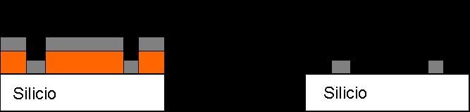
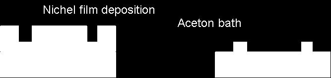
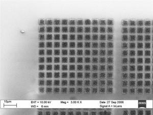
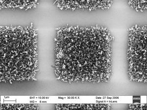
6 Patternization


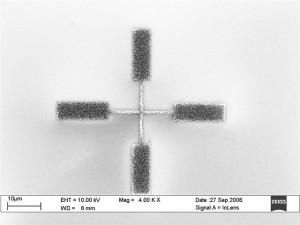
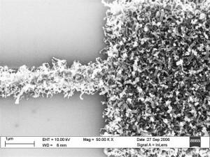
7 Sapphire Comb-like electrodes Electrodes Microstrip Pt 100 µm Si3N4 Silicon Aluminium Sapphire Silicon Quartz GEOMETRY and SUBSTRATES
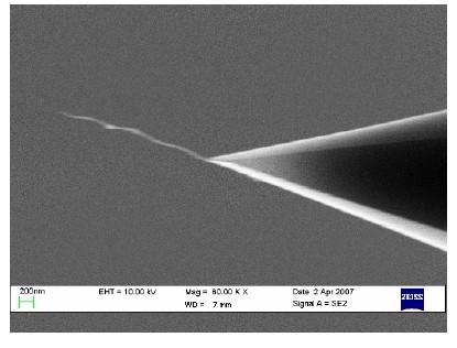
8 Radiation detector made of Multi-Walled Carbon Nanotubes 30 nm P t Si3N4 CNT 100 µm 500 µm Sapphire Au + Pt 250 nm Dark current 10 ps pulse shape Laser 355 nm 532 nm 1064 nm CNT 50 Ω Drain voltage Oscillograph Im p No ortan am si g t : n pli f i c al at i on World first A. Ambrosio et al: A prototype of a Carbon Nanotube microstrip radiation detector, Nuclear Instruments and Methods in Physics Research A 589 (2008)
9 Signals detected with the first carbon nanotube radiation detector
10 Signal comparison at different wawelenghts

11 Collected electrons / incident photons (E-06) Collected electrons / incident photons No signal amplification No CNT annealing.. as cast MWCNT
12 CNT absorbance (log10 1/T)
13 Photocurrent vs λ small area whole area 0.3 Absorbance Photon energy (ev) absorbance InorX 10 (As) 0.7 Photocurrent normalized to the number of photons Inor vs photon energy, obtained illuminating the whole surface of a MWCNT sample with filtered light ( ) as well as small part of the surface with laser spots (*). Continuous line indicates the absorbance spectrum of the same MWCNT sample. M. Passacantando et al: Photoconductivity in defective carbon nanotube sheets under ultraviolet visible near infrared radiation, APPLIED PHYSICS LETTERS 93,
14 The main problem Signal generated inside CNTs is collected by means of electrodes in a plane orthogonal to the nanotube axis. The charge must migrate by tunneling and has a great probability to be reabsorbed. The efficiency of such device is very low.
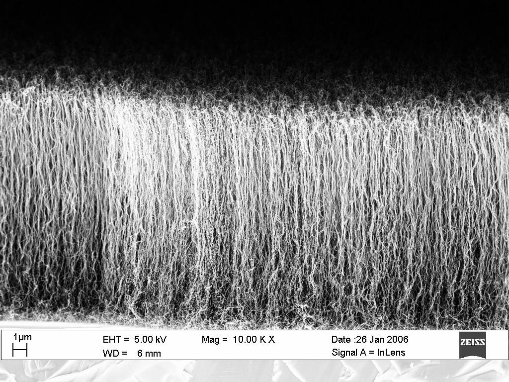
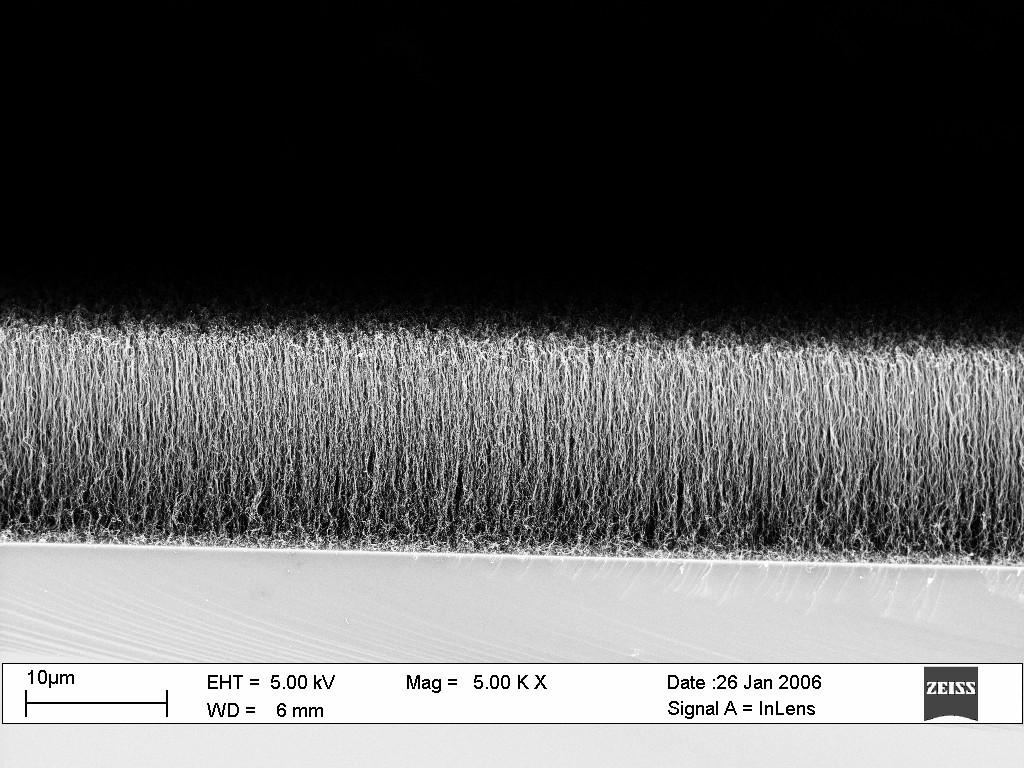
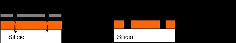
15 A different architecture under test Dark current Nanotubes growth on a silicon substrate may create a diode-like junction with surprising photoresponsivity properties. With this architecture the charge generated inside CNTs by radiation can be collected trough the silicon substrate without great attenuation.
16 The answer of detector to a pulsed red light
17 Measured photocurrent
 Conversion efficiency")
18 Collected electrons / incident photons (E-06) Conversion efficiency Sapphire
19 Conclusion CNTs demonstrate important photoconductive properties; The maximum sensitivity is in the UV region; The first microstrip detector made of multi- walled carbon nanotubes grown on sapphire substrate have been realized.
20 Next Study of new architecture with CNTs grown on silicon substrate; Charge amplification inside the silicon substrate; Nanotubes coating.

21 INFN & University of L Aquila Bari Napoli Perugia Roma 2 Development of UV Single Photon Detector based on Carbon Nanotubes Funded by INFN for the three-year period
Carbon Nanotubes in Interconnect Applications
 Carbon Nanotubes in Interconnect Applications Page 1 What are Carbon Nanotubes? What are they good for? Why are we interested in them? - Interconnects of the future? Comparison of electrical properties
Supplementary material for High responsivity mid-infrared graphene detectors with antenna-enhanced photo-carrier generation and collection
 Supplementary material for High responsivity mid-infrared graphene detectors with antenna-enhanced photo-carrier generation and collection Yu Yao 1, Raji Shankar 1, Patrick Rauter 1, Yi Song 2, Jing Kong
Carbon Nanotubes for Interconnect Applications Franz Kreupl, Andrew P. Graham, Maik Liebau, Georg S. Duesberg, Robert Seidel, Eugen Unger
 Carbon Nanotubes for Interconnect Applications Franz Kreupl, Andrew P. Graham, Maik Liebau, Georg S. Duesberg, Robert Seidel, Eugen Unger Infineon Technologies Corporate Research Munich, Germany Outline
What are Carbon Nanotubes? What are they good for? Why are we interested in them?
 Growth and Properties of Multiwalled Carbon Nanotubes What are Carbon Nanotubes? What are they good for? Why are we interested in them? - Interconnects of the future? - our vision Where do we stand - our
Supplementary Figure 1 XRD pattern of a defective TiO 2 thin film deposited on an FTO/glass substrate, along with an XRD pattern of bare FTO/glass
 Supplementary Figure 1 XRD pattern of a defective TiO 2 thin film deposited on an FTO/glass substrate, along with an XRD pattern of bare FTO/glass and a reference pattern of anatase TiO 2 (JSPDS No.: 21-1272).
Theoretical Modeling of a photodetector based on ballistic Carbone nanotube with VHDL-AMS M. Troudi 2, A. Mahmoudi 1, N. Sghaier 1,2,a A.
 International Letters of Chemistry, Physics and Astronomy Online: 2015-07-03 ISSN: 2299-3843, Vol. 55, pp 112-118 doi:10.18052/www.scipress.com/ilcpa.55.112 2015 SciPress Ltd., Switzerland Theoretical
EE 5344 Introduction to MEMS CHAPTER 5 Radiation Sensors
 EE 5344 Introduction to MEMS CHAPTER 5 Radiation Sensors 5. Radiation Microsensors Radiation µ-sensors convert incident radiant signals into standard electrical out put signals. Radiant Signals Classification
Metallic: 2n 1. +n 2. =3q Armchair structure always metallic = 2
 Properties of CNT d = 2.46 n 2 2 1 + n1n2 + n2 2π Metallic: 2n 1 +n 2 =3q Armchair structure always metallic a) Graphite Valence(π) and Conduction(π*) states touch at six points(fermi points) Carbon Nanotube:
EN2912C: Future Directions in Computing Lecture 08: Overview of Near-Term Emerging Computing Technologies
 EN2912C: Future Directions in Computing Lecture 08: Overview of Near-Term Emerging Computing Technologies Prof. Sherief Reda Division of Engineering Brown University Fall 2008 1 Near-term emerging computing
Carbon Nanomaterials
 Carbon Nanomaterials STM Image 7 nm AFM Image Fullerenes C 60 was established by mass spectrographic analysis by Kroto and Smalley in 1985 C 60 is called a buckminsterfullerene or buckyball due to resemblance
Carbon Nanotube Electronics
 Carbon Nanotube Electronics Jeorg Appenzeller, Phaedon Avouris, Vincent Derycke, Stefan Heinz, Richard Martel, Marko Radosavljevic, Jerry Tersoff, Shalom Wind H.-S. Philip Wong hspwong@us.ibm.com IBM T.J.
Graphene photodetectors with ultra-broadband and high responsivity at room temperature
 SUPPLEMENTARY INFORMATION DOI: 10.1038/NNANO.2014.31 Graphene photodetectors with ultra-broadband and high responsivity at room temperature Chang-Hua Liu 1, You-Chia Chang 2, Ted Norris 1.2* and Zhaohui
OPTI510R: Photonics. Khanh Kieu College of Optical Sciences, University of Arizona Meinel building R.626
 OPTI510R: Photonics Khanh Kieu College of Optical Sciences, University of Arizona kkieu@optics.arizona.edu Meinel building R.626 Announcements Homework #6 is assigned, due May 1 st Final exam May 8, 10:30-12:30pm
SUPPLEMENTARY INFORMATION
 Supplementary Information: Photocurrent generation in semiconducting and metallic carbon nanotubes Maria Barkelid 1*, Val Zwiller 1 1 Kavli Institute of Nanoscience, Delft University of Technology, Delft,
Chapter 7. Solar Cell
 Chapter 7 Solar Cell 7.0 Introduction Solar cells are useful for both space and terrestrial application. Solar cells furnish the long duration power supply for satellites. It converts sunlight directly
Electrostatic Single-walled Carbon Nanotube (CNT) Field Effect Transistor Device Modeling
 Field Effect Transistor Device Modeling") Electrostatic Single-walled Carbon Nanotube (CNT) Field Effect Transistor Device Modeling Henok Abebe The Service USC Viterbi School of Engineering Information Sciences Institute Collaborator Ellis Cumberbatch
Electrostatic Single-walled Carbon Nanotube (CNT) Field Effect Transistor Device Modeling Henok Abebe The Service USC Viterbi School of Engineering Information Sciences Institute Collaborator Ellis Cumberbatch
UvA-DARE (Digital Academic Repository) Charge carrier dynamics in photovoltaic materials Jensen, S.A. Link to publication
 Charge carrier dynamics in photovoltaic materials Jensen, S.A. Link to publication") UvA-DARE (Digital Academic Repository) Charge carrier dynamics in photovoltaic materials Jensen, S.A. Link to publication Citation for published version (APA): Jensen, S. A. (2014). Charge carrier dynamics
UvA-DARE (Digital Academic Repository) Charge carrier dynamics in photovoltaic materials Jensen, S.A. Link to publication Citation for published version (APA): Jensen, S. A. (2014). Charge carrier dynamics
Determining Carbon Nanotube Properties from Raman. Scattering Measurements
 Determining Carbon Nanotube Properties from Raman Scattering Measurements Ying Geng 1, David Fang 2, and Lei Sun 3 1 2 3 The Institute of Optics, Electrical and Computer Engineering, Laboratory for Laser
I-V characteristics model for Carbon Nanotube Field Effect Transistors
 International Journal of Engineering & Technology IJET-IJENS Vol:14 No:04 33 I-V characteristics model for Carbon Nanotube Field Effect Transistors Rebiha Marki, Chérifa Azizi and Mourad Zaabat. Abstract--
Graphene and Carbon Nanotubes
 Graphene and Carbon Nanotubes 1 atom thick films of graphite atomic chicken wire Novoselov et al - Science 306, 666 (004) 100μm Geim s group at Manchester Novoselov et al - Nature 438, 197 (005) Kim-Stormer
Fabrication of Carbon Nanotube Channels on Three- Dimensional Building Blocks and Their Applications
 AOARD Report Fabrication of Carbon Nanotube Channels on Three- Dimensional Building Blocks and Their Applications Principal Investigator : Haiwon Lee Grant Number : AOARD 104106 Affiliation of Researcher(s):
SUPPLEMENTARY INFORMATION
 SUPPLEMENTARY INFORMATION Flexible, high-performance carbon nanotube integrated circuits Dong-ming Sun, Marina Y. Timmermans, Ying Tian, Albert G. Nasibulin, Esko I. Kauppinen, Shigeru Kishimoto, Takashi
Carbon nanotubes and Graphene
 16 October, 2008 Solid State Physics Seminar Main points 1 History and discovery of Graphene and Carbon nanotubes 2 Tight-binding approximation Dynamics of electrons near the Dirac-points 3 Properties
Introduction to Nanotechnology Chapter 5 Carbon Nanostructures Lecture 1
 Introduction to Nanotechnology Chapter 5 Carbon Nanostructures Lecture 1 ChiiDong Chen Institute of Physics, Academia Sinica chiidong@phys.sinica.edu.tw 02 27896766 Section 5.2.1 Nature of the Carbon Bond
In today s lecture, we will cover:
 In today s lecture, we will cover: Metal and Metal oxide Nanoparticles Semiconductor Nanocrystals Carbon Nanotubes 1 Week 2: Nanoparticles Goals for this section Develop an understanding of the physical
Manipulating and determining the electronic structure of carbon nanotubes
 Manipulating and determining the electronic structure of carbon nanotubes (06.12.2005 NTHU, Physics Department) Po-Wen Chiu Department of Electrical Engineering, Tsing Hua University, Hsinchu, Taiwan Max-Planck
Dual readout with tiles for calorimetry.
 Dual readout with tiles for calorimetry. F.Lacava on behalf of the RD52 / DREAM Collaboration Cagliari Cosenza Iowa State Pavia Pisa Roma 1 Texas Tech. 13th Topical Seminar on Innovative Particle and Radiation
Manufacture of Nanostructures for Power Electronics Applications
 Manufacture of Nanostructures for Power Electronics Applications Brian Hunt and Jon Lai Etamota Corporation 2672 E. Walnut St. Pasadena, CA 91107 APEC, Palm Springs Feb. 23rd, 2010 1 Background Outline
Confocal Microscope Imaging of Single-Emitter Fluorescence and Photon Antibunching
 Confocal Microscope Imaging of Single-Emitter Fluorescence and Photon Antibunching By Dilyana Mihaylova Abstract The purpose of this lab is to study different types of single emitters including quantum
Modelling of Diamond Devices with TCAD Tools
 RADFAC Day - 26 March 2015 Modelling of Diamond Devices with TCAD Tools A. Morozzi (1,2), D. Passeri (1,2), L. Servoli (2), K. Kanxheri (2), S. Lagomarsino (3), S. Sciortino (3) (1) Engineering Department
Carbon Nanotubes (CNTs)
") Carbon Nanotubes (s) Seminar: Quantendynamik in mesoskopischen Systemen Florian Figge Fakultät für Physik Albert-Ludwigs-Universität Freiburg July 7th, 2010 F. Figge (University of Freiburg) Carbon Nanotubes
Carbon Nanotubes (s) Seminar: Quantendynamik in mesoskopischen Systemen Florian Figge Fakultät für Physik Albert-Ludwigs-Universität Freiburg July 7th, 2010 F. Figge (University of Freiburg) Carbon Nanotubes
ELECTRONIC DEVICES AND CIRCUITS SUMMARY
 ELECTRONIC DEVICES AND CIRCUITS SUMMARY Classification of Materials: Insulator: An insulator is a material that offers a very low level (or negligible) of conductivity when voltage is applied. Eg: Paper,
Recap (so far) Low-Dimensional & Boundary Effects
 Low-Dimensional & Boundary Effects") Recap (so far) Ohm s & Fourier s Laws Mobility & Thermal Conductivity Heat Capacity Wiedemann-Franz Relationship Size Effects and Breakdown of Classical Laws 1 Low-Dimensional & Boundary Effects Energy
Recap (so far) Ohm s & Fourier s Laws Mobility & Thermal Conductivity Heat Capacity Wiedemann-Franz Relationship Size Effects and Breakdown of Classical Laws 1 Low-Dimensional & Boundary Effects Energy
Photoresponsive Nanoscale Columnar Transistors
 Photoresponsive Nanoscale Columnar Transistors Xuefeng Guo, Shengxiong Xiao, Matthew Myers, Qian Miao, Michael L. Steigerwald, and Colin Nuckolls. Center for Nanochemistry, Beijing National Laboratory
Electrostatics of Nanowire Transistors
 Electrostatics of Nanowire Transistors Jing Guo, Jing Wang, Eric Polizzi, Supriyo Datta and Mark Lundstrom School of Electrical and Computer Engineering Purdue University, West Lafayette, IN, 47907 ABSTRACTS
ELEC 4700 Assignment #2
 ELEC 4700 Assignment #2 Question 1 (Kasop 4.2) Molecular Orbitals and Atomic Orbitals Consider a linear chain of four identical atoms representing a hypothetical molecule. Suppose that each atomic wavefunction
Supplementary Figure 1. Selected area electron diffraction (SAED) of bilayer graphene and tblg. (a) AB
 of bilayer graphene and tblg. (a) AB") Supplementary Figure 1. Selected area electron diffraction (SAED) of bilayer graphene and tblg. (a) AB stacked bilayer graphene (b), (c), (d), (e), and (f) are twisted bilayer graphene with twist angle
Supplementary Figure 1. Selected area electron diffraction (SAED) of bilayer graphene and tblg. (a) AB stacked bilayer graphene (b), (c), (d), (e), and (f) are twisted bilayer graphene with twist angle
Chemistry Instrumental Analysis Lecture 8. Chem 4631
 Chemistry 4631 Instrumental Analysis Lecture 8 UV to IR Components of Optical Basic components of spectroscopic instruments: stable source of radiant energy transparent container to hold sample device
CHAPTER 4 THE EXPERIMENTAL RESULTS AND DISCUSSIONS 4.1 THE ENVIRONMENT SETUP FOR MEASUREMENT
 CHAPTER 4 THE EXPERIMENTAL RESULTS AND DISCUSSIONS 4.1 THE ENVIRONMENT SETUP FOR MEASUREMENT After fabrication, the silicon oxide substrate was observed and evaluated by using scanning electron microscopy
The Electromagnetic Properties of Materials
 The Electromagnetic Properties of Materials Electrical conduction Metals Semiconductors Insulators (dielectrics) Superconductors Magnetic materials Ferromagnetic materials Others Photonic Materials (optical)
Single Photon detectors
 Single Photon detectors Outline Motivation for single photon detection Semiconductor; general knowledge and important background Photon detectors: internal and external photoeffect Properties of semiconductor
3.1 Absorption and Transparency
 3.1 Absorption and Transparency 3.1.1 Optical Devices (definitions) 3.1.2 Photon and Semiconductor Interactions 3.1.3 Photon Intensity 3.1.4 Absorption 3.1 Absorption and Transparency Objective 1: Recall
Electronic Supplementary Information for
 Electronic Supplementary Material (ESI) for Journal of Materials Chemistry C. This journal is The Royal Society of Chemistry 018 Electronic Supplementary Information for Broadband Photoresponse Based on
2D Materials for Gas Sensing
 2D Materials for Gas Sensing S. Guo, A. Rani, and M.E. Zaghloul Department of Electrical and Computer Engineering The George Washington University, Washington DC 20052 Outline Background Structures of
ABSTRACT. p-n Junction Photodetectors Based on Macroscopic Single-Wall Carbon Nanotube Films. Xiaowei He
 ABSTRACT p-n Junction Photodetectors Based on Macroscopic Single-Wall Carbon Nanotube Films by Xiaowei He Single-Wall carbon nanotubes (SWCNTs) are promising for use in solar cells and photodetectors because
NANO TECHNOLOGY IN POLYMER SOLAR CELLS. Mayur Padharia, Hardik Panchal, Keval Shah, *Neha Patni, Shibu.G.Pillai
 NANO TECHNOLOGY IN POLYMER SOLAR CELLS Mayur Padharia, Hardik Panchal, Keval Shah, *Neha Patni, Shibu.G.Pillai Department of Chemical Engineering, Institute of Technology, Nirma University, S. G. Highway,
ECE 474: Principles of Electronic Devices. Prof. Virginia Ayres Electrical & Computer Engineering Michigan State University
 ECE 474: Principles of Electronic Devices Prof. Virginia Ayres Electrical & Computer Engineering Michigan State University ayresv@msu.edu Lecture 07: Quantify physical structures of crystal systems that
SEU RADIATION EFFECTS ON GAA-CNTFET BASED DIGITAL LOGIC CIRCUIT
 International Journal of Mechanical Engineering and Technology (IJMET) Volume 9, Issue 7, July 2018, pp. 345 353, Article ID: IJMET_09_07_039 Available online at http://www.iaeme.com/ijmet/issues.asp?jtype=ijmet&vtype=9&itype=7
Because light behaves like a wave, we can describe it in one of two ways by its wavelength or by its frequency.
 Light We can use different terms to describe light: Color Wavelength Frequency Light is composed of electromagnetic waves that travel through some medium. The properties of the medium determine how light
GRAPHENE NANORIBBONS Nahid Shayesteh,
 USC Department of Physics Graduate Seminar 1 GRAPHENE NANORIBBONS Nahid Shayesteh, Outlines 2 Carbon based material Discovery and innovation of graphen Graphene nanoribbons structure Application of Graphene
Heat/phonons Transport in Nanostructures and Phononics
 ELTE, Budapest 14 May, 2009 Heat/phonons Transport in Nanostructures and Phononics LI Baowen ( 李保文 ) Centre for Computational Science and Engineering, FOS, & Department of Physics NUS Graduate School for
Two-Dimensional CH 3 NH 3 PbI 3 Perovskite: Synthesis and Optoelectronic Application
 Two-Dimensional CH 3 NH 3 PbI 3 Perovskite: Synthesis and Optoelectronic Application Jingying Liu,, Yunzhou Xue,,, Ziyu Wang,, Zai-Quan Xu, Changxi Zheng, Bent Weber, Jingchao Song, Yusheng Wang, Yuerui
Novel Dispersion and Self-Assembly
 Novel Dispersion and Self-Assembly of Carbon Nanotubes Mohammad F. Islam 100g Department of Chemical Engineering and Department of Materials Science & Engineering Funding Agencies http://islamgroup.cheme.cmu.edu
Electrical and Optical Properties. H.Hofmann
 Introduction to Nanomaterials Electrical and Optical Properties H.Hofmann Electrical Properties Ohm: G= σw/l where is the length of the conductor, measured in meters [m], A is the cross-section area of
Strong-electric-field effects and antenna resonances in single-wall carbon nanotube films
 Strong-electric-field effects and antenna resonances in single-wall carbon nanotube films Dalius Seliuta Center for Physical Sciences and Technology, Vilnius, Lithuania Liudas Subačius, Irmantas Kašalynas,
CHAPTER 11 Semiconductor Theory and Devices
 CHAPTER 11 Semiconductor Theory and Devices 11.1 Band Theory of Solids 11.2 Semiconductor Theory 11.3 Semiconductor Devices 11.4 Nanotechnology It is evident that many years of research by a great many
Boron-based semiconductor solids as thermal neutron detectors
 Boron-based semiconductor solids as thermal neutron detectors Douglas S. McGregor 1 and Stan M. Vernon 2 1 S.M.A.R.T. Laboratory, Department of Nuclear Engineering and Radiological Sciences, University
Laser Basics. What happens when light (or photon) interact with a matter? Assume photon energy is compatible with energy transition levels.
 interact with a matter? Assume photon energy is compatible with energy transition levels.") What happens when light (or photon) interact with a matter? Assume photon energy is compatible with energy transition levels. Electron energy levels in an hydrogen atom n=5 n=4 - + n=3 n=2 13.6 = [ev]
What happens when light (or photon) interact with a matter? Assume photon energy is compatible with energy transition levels. Electron energy levels in an hydrogen atom n=5 n=4 - + n=3 n=2 13.6 = [ev]
Nanocarbon Technology for Development of Innovative Devices
 Nanocarbon Technology for Development of Innovative Devices Shintaro Sato Daiyu Kondo Shinichi Hirose Junichi Yamaguchi Graphene, a one-atom-thick honeycomb lattice made of carbon, and a carbon nanotube,
2 Symmetry. 2.1 Structure of carbon nanotubes
 2 Symmetry Carbon nanotubes are hollow cylinders of graphite sheets. They can be viewed as single molecules, regarding their small size ( nm in diameter and µm length), or as quasi-one dimensional crystals
Magnetic and optic sensing. Magnetic sensors
 Magnetic and optic sensing Magnetic sensors 1 Literature Physics of Semiconductor Devices S.M. Sze, Kwok K. Ng Available as ebook on http://www.lub.lu.se/en/search/lubsearch.ht ml This lecture chapters
Diameter Optimization for Highest Degree of Ballisticity of Carbon Nanotube Field Effect Transistors I. Khan, O. Morshed and S. M.
 Diameter Optimization for Highest Degree of Ballisticity of Carbon Nanotube Field Effect Transistors I. Khan, O. Morshed and S. M. Mominuzzaman Department of Electrical and Electronic Engineering, Bangladesh
SUPPLEMENTARY INFORMATION
 In the format provided by the authors and unedited. DOI: 10.1038/NNANO.2017.46 Position dependent and millimetre-range photodetection in phototransistors with micrometre-scale graphene on SiC Biddut K.
Device 3D. 3D Device Simulator. Nano Scale Devices. Fin FET
 Device 3D 3D Device Simulator Device 3D is a physics based 3D device simulator for any device type and includes material properties for the commonly used semiconductor materials in use today. The physical
Supporting Information
 Photothermal Effect Induced Negative Photoconductivity and High Responsivity in Flexible Black Phosphorus Transistors Jinshui Miao,, Bo Song,, Qing Li, Le Cai, Suoming Zhang, Weida Hu, Lixin Dong, Chuan
DEPFET sensors development for the Pixel Detector of BELLE II
 DEPFET sensors development for the Pixel Detector of BELLE II 13 th Topical Seminar on Innovative Particle and Radiation Detectors (IPRD13) 7 10 October 2013, Siena, Italy Paola Avella for the DEPFET collaboration
CCD OPERATION. The BBD was an analog delay line, made up of capacitors such that an analog signal was moving along one step at each clock cycle.
 CCDS Lesson 4 CCD OPERATION The predecessor of the CCD was a device called the BUCKET BRIGADE DEVICE developed at the Phillips Research Labs The BBD was an analog delay line, made up of capacitors such
Simulation of AlGaN/Si and InN/Si ELECTRIC DEVICES
 Simulation of AlGaN/Si and InN/Si ELECTRIC DEVICES Zehor Allam 1, Abdelkader Hamdoune 2, Chahrazed Boudaoud 3, Asmaa Amrani 4,Aicha Soufi 5,Zakia Nakoul 6 Unity of Research Materials and Renewable Energies,
Carbon Nanotubes. Seminar report. Submitted in partial fulfillment of the requirement for the award of degree of Mechanical.
 A Seminar report On Carbon Nanotubes Submitted in partial fulfillment of the requirement for the award of degree of Mechanical SUBMITTED TO: SUBMITTED BY: www.studymafia.org www.studymafia.org Preface
Electronic and Photonic Applications of One- Dimensional Carbon and Silicon Nanostructures
 Electronic and Photonic Applications of One- Dimensional Carbon and Silicon Nanostructures Anupama B. Kaul Jet Propulsion Laboratory, California Institute of Technology, Pasadena, CA 91109 Ph: (818) 393-7186;
Title: Ultrafast photocurrent measurement of the escape time of electrons and holes from
 Title: Ultrafast photocurrent measurement of the escape time of electrons and holes from carbon nanotube PN junction photodiodes Authors: Nathaniel. M. Gabor 1,*, Zhaohui Zhong 2, Ken Bosnick 3, Paul L.
Plasmonic Hot Hole Generation by Interband Transition in Gold-Polyaniline
 Supplementary Information Plasmonic Hot Hole Generation by Interband Transition in Gold-Polyaniline Tapan Barman, Amreen A. Hussain, Bikash Sharma, Arup R. Pal* Plasma Nanotech Lab, Physical Sciences Division,
Quantized Electrical Conductance of Carbon nanotubes(cnts)
") Quantized Electrical Conductance of Carbon nanotubes(cnts) By Boxiao Chen PH 464: Applied Optics Instructor: Andres L arosa Abstract One of the main factors that impacts the efficiency of solar cells is
Quantized Electrical Conductance of Carbon nanotubes(cnts) By Boxiao Chen PH 464: Applied Optics Instructor: Andres L arosa Abstract One of the main factors that impacts the efficiency of solar cells is
1. Nanotechnology & nanomaterials -- Functional nanomaterials enabled by nanotechnologies.
 Novel Nano-Engineered Semiconductors for Possible Photon Sources and Detectors NAI-CHANG YEH Department of Physics, California Institute of Technology 1. Nanotechnology & nanomaterials -- Functional nanomaterials
Electric Field-Dependent Charge-Carrier Velocity in Semiconducting Carbon. Nanotubes. Yung-Fu Chen and M. S. Fuhrer
 Electric Field-Dependent Charge-Carrier Velocity in Semiconducting Carbon Nanotubes Yung-Fu Chen and M. S. Fuhrer Department of Physics and Center for Superconductivity Research, University of Maryland,
Nanostructures. Lecture 13 OUTLINE
 Nanostructures MTX9100 Nanomaterials Lecture 13 OUTLINE -What is quantum confinement? - How can zero-dimensional materials be used? -What are one dimensional structures? -Why does graphene attract so much
Transient Photocurrent Measurements of Graphene Related Materials
 Transient Photocurrent Measurements of Graphene Related Materials P. Srinivasa Rao Mentor: Prof. dr. Gvido Bratina Laboratory of Organic Matter Physics University of Nova Gorica 1 Contents: 1. Electrical
Supplementary Information
 Electronic Supplementary Material (ESI) for Physical Chemistry Chemical Physics. This journal is the Owner Societies 2015 Supplementary Information Vertical Heterostructures of MoS2 and Graphene Nanoribbons
THz experiments at the UCSB FELs and the THz Science and Technology Network.
 THz experiments at the UCSB FELs and the THz Science and Technology Network. Mark Sherwin UCSB Physics Department and Institute for Quantum and Complex Dynamics UCSB Center for Terahertz Science and Technology
Nanomaterials for Plasmonic Devices. Lih J. Chen
 Nanomaterials for Plasmonic Devices Lih J. Chen Department of Materials Science and Engineering, National Tsing Hua University, Hsinchu, Taiwan Papers on Plasmon: 75,000 (6/25/2018) Papers on Plasmonics:
25 Instruments for Optical Spectrometry
 25 Instruments for Optical Spectrometry 25A INSTRUMENT COMPONENTS (1) source of radiant energy (2) wavelength selector (3) sample container (4) detector (5) signal processor and readout (a) (b) (c) Fig.
Electro-Thermal Transport in Silicon and Carbon Nanotube Devices E. Pop, D. Mann, J. Rowlette, K. Goodson and H. Dai
 Electro-Thermal Transport in Silicon and Carbon Nanotube Devices E. Pop, D. Mann, J. Rowlette, K. Goodson and H. Dai E. Pop, 1,2 D. Mann, 1 J. Rowlette, 2 K. Goodson 2 and H. Dai 1 Dept. of 1 Chemistry
Quantised Thermal Conductance
 B B Quantised Thermal Conductance In 1983 J Pendry published a paper on the quantum limits to the flow of information and entropy [Pendry'83]. In it he showed that there is an inequality that limits the
UNIVERSITY OF CALIFORNIA College of Engineering Department of Electrical Engineering and Computer Sciences. EECS 130 Professor Ali Javey Fall 2006
 UNIVERSITY OF CALIFORNIA College of Engineering Department of Electrical Engineering and Computer Sciences EECS 130 Professor Ali Javey Fall 2006 Midterm 2 Name: SID: Closed book. Two sheets of notes are
Nanomaterials Electrical and Optical Properties
 Nanomaterials Electrical and Optical Properties H.Hofmann ÉCOLE POLYTECHNIQUE FÉDÉRALE DE LAUSANNE Electrical Properties Energy LUMO HOMO Forbidden bandgap Atom Mo lecule Cluster Nanoparticle Semi conductor
Photon Instrumentation. First Mexican Particle Accelerator School Guanajuato Oct 6, 2011
 Photon Instrumentation First Mexican Particle Accelerator School Guanajuato Oct 6, 2011 Outline The Electromagnetic Spectrum Photon Detection Interaction of Photons with Matter Photoelectric Effect Compton
UNIT I: Electronic Materials.
 SIDDHARTH INSTITUTE OF ENGINEERING & TECHNOLOGY :: PUTTUR Siddharth Nagar, Narayanavanam Road 517583 QUESTION BANK (DESCRIPTIVE) Subject with Code: SEMICONDUCTOR PHYSICS (18HS0851) Course & Branch: B.Tech
GaN for use in harsh radiation environments
 4 th RD50 - Workshop on radiation hard semiconductor devices for very high luminosity colliders GaN for use in harsh radiation environments a (W Cunningham a, J Grant a, M Rahman a, E Gaubas b, J Vaitkus
Photoluminescence and Raman Spectroscopy on truncated Nano Pyramids
 Photoluminescence and Raman Spectroscopy on truncated Nano Pyramids Physics of low Dimensions, FFF042 Josefin Voigt & Stefano Scaramuzza 10.12.2013, Lund University 1 Introduction In this project truncated
LASERS. Dr D. Arun Kumar Assistant Professor Department of Physical Sciences Bannari Amman Institute of Technology Sathyamangalam
 LASERS Dr D. Arun Kumar Assistant Professor Department of Physical Sciences Bannari Amman Institute of Technology Sathyamangalam General Objective To understand the principle, characteristics and types
(Co-PIs-Mark Brongersma, Yi Cui, Shanhui Fan) Stanford University. GCEP Research Symposium 2013 Stanford, CA October 9, 2013
 Stanford University. GCEP Research Symposium 2013 Stanford, CA October 9, 2013") High-efficiency thin film nano-structured multi-junction solar James S. cells Harris (PI) (Co-PIs-Mark Brongersma, Yi Cui, Shanhui Fan) Stanford University GCEP Research Symposium 2013 Stanford, CA October
High-efficiency thin film nano-structured multi-junction solar James S. cells Harris (PI) (Co-PIs-Mark Brongersma, Yi Cui, Shanhui Fan) Stanford University GCEP Research Symposium 2013 Stanford, CA October
Supporting Information
 Electronic Supplementary Material (ESI) for ChemComm. This journal is The Royal Society of Chemistry 2014 Supporting Information Controllable Atmospheric Pressure Growth of Mono-layer, Bi-layer and Tri-layer
CLASS 12th. Modern Physics-I
 CLASS 12th Modern Physics-I Modern Physics-I 01. Dual Nature of Radiation The phenomena such as interference, diffraction and polarization were success-fully explained on the basis of were nature of On
Carbon-Based Electronics: Will there be a carbon age to follow the silicon age? Jeffrey Bokor EECS Department UC Berkeley
 Carbon-Based Electronics: Will there be a carbon age to follow the silicon age? Jeffrey Bokor EECS Department UC Berkeley jbokor@eecs.berkeley.edu Solid State Seminar 9-13-13 1 Outline Review of development
Laser heating of noble gas droplet sprays: EUV source efficiency considerations
 Laser heating of noble gas droplet sprays: EUV source efficiency considerations S.J. McNaught, J. Fan, E. Parra and H.M. Milchberg Institute for Physical Science and Technology University of Maryland College
Planar Organic Photovoltaic Device. Saiful I. Khondaker
 Planar Organic Photovoltaic Device Saiful I. Khondaker Nanoscience Technology Center and Department of Physics University of Central Florida http://www.physics.ucf.edu/~khondaker W Metal 1 L ch Metal 2
Nonlinear ultrafast fiber optic devices based on Carbon Nanotubes
 Nonlinear ultrafast fiber optic devices based on Carbon Nanotubes Guillermo E. Villanueva, Claudio J. Oton Michael B. Jakubinek, Benoit Simard,, Jaques Albert, Pere Pérez-Millán Outline Introduction CNT-coated
Graphene and new 2D materials: Opportunities for High Frequencies applications
 Graphene and new 2D materials: Opportunities for High Frequencies applications April 21th, 2015 H. Happy, E. Pallecchi, B. Plaçais, D. Jiménez, R. Sordan, D. Neumaier Graphene Flagship WP4 HF electronic
Ultralow-Power Reconfigurable Computing with Complementary Nano-Electromechanical Carbon Nanotube Switches
 Ultralow-Power Reconfigurable Computing with Complementary Nano-Electromechanical Carbon Nanotube Switches Presenter: Tulika Mitra Swarup Bhunia, Massood Tabib-Azar, and Daniel Saab Electrical Eng. And
Energetic particles and their detection in situ (particle detectors) Part II. George Gloeckler
 Part II. George Gloeckler") Energetic particles and their detection in situ (particle detectors) Part II George Gloeckler University of Michigan, Ann Arbor, MI University of Maryland, College Park, MD Simple particle detectors Gas-filled
Energetic particles and their detection in situ (particle detectors) Part II George Gloeckler University of Michigan, Ann Arbor, MI University of Maryland, College Park, MD Simple particle detectors Gas-filled