CHAPTER 4 THE EXPERIMENTAL RESULTS AND DISCUSSIONS 4.1 THE ENVIRONMENT SETUP FOR MEASUREMENT
|
|
|
- Shawn Washington
- 5 years ago
- Views:
Transcription
1 CHAPTER 4 THE EXPERIMENTAL RESULTS AND DISCUSSIONS 4.1 THE ENVIRONMENT SETUP FOR MEASUREMENT After fabrication, the silicon oxide substrate was observed and evaluated by using scanning electron microscopy (SEM) images at each stage of the procedure. The SEM was performed with JSM-6500F high-resolution scanning microscope. In addition to surface structure observation, the photo-sensing properties of the nanodevice were also verified by using laser diode as illumination light source. The environment setup for I-V characteristics measurement was shown in Fig The laser diode, laser diodes driver, optical measurement table and the clean room are all in Professor Eric Diau s Femtochemistry Laboratory. The laser diode driver is PicoQuant POL 800D and the 375 nm, 400 nm, 435 nm laser diodes are PicoQuant LDH-P-C375, 400, 435. The current meter is Keithley V SourceMeter. The PCB on which the nanodevice-modified silicon chip was located was put in the vacuum chamber or normal room condition when measuring the I-V characteristics. During the measurement, the environment was kept in dark except the laser diode. We also measured the UV-visible and Photoluminescence (PL) spectra to confirm the specific optical characteristics of the nanostructure. The measurement instruments are all in Professor Teng-Ming Chen s Phosphors Research Laboratory. The UV-visible absorbance spectrum analysis was performed with Hitachi-U-3010 Spectrophotometer. The detecting wavelength was in the range of 190 nm to 1000 nm, and according the transmitted of sample, it s absorption spectra is monitored by Beer s Law. The typical experimental setup is shown in Fig A beam of light from a visible and/or UV light source (red colored) is separated into its component wavelengths by a prism or diffraction grating. Each monochromatic (single wavelength) beam in turn is split into two equal intensity beams by a half-mirrored device. One beam, the sample beam (colored magenta), passes 51
2 through a small transparent container (cuvette) containing a solution of the compound being studied in a transparent solvent. The other beam, the reference (colored blue), passes through an identical cuvette containing only the solvent. The intensities of these light beams are then measured by electronic detectors and compared. The intensity of the reference beam, which should have suffered little or no light absorption, is defined as I 0. The intensity of the sample beam is defined as I. Over a short period of time, the spectrometer automatically scans all the component wavelengths in the manner described. The ultraviolet (UV) region scanned is normally from 200 to 400 nm, and the visible portion is from 400 to 800 nm. If the sample compound does not absorb light of a given wavelength, I = I 0. However, if the sample compound absorbs light then I is less than I 0, and this difference may be plotted on a graph versus wavelength. Absorption may be presented as transmittance (T = I/I 0 ) or absorbance (A = log I 0 /I). If no absorption has occurred, T = 1.0 and A = 0. Most spectrometers display absorbance on the vertical axis, and the commonly observed range is from 0 (100% transmittance) to 2 (1% transmittance). The PL spectrometer analysis is performed with Jobin Yvon Instrument S. A. Inc. Spectrometer. The scanning range is from 200 nm to 1000 nm. The typical experimental setup for PL intensity spectrum measurement is shown in Fig When light of sufficient energy is incident on a material, photons are absorbed and excite the electrons from ground state. If radiative relaxation occurs, the emitted light is called photoluminescence (PL). This light can be collected and analyzed to yield a wealth of information about the photo-excitation nanostructure. In this experiment, we used laser source with different wavelengths to photo-activate the nanostructures. Subsequently, the emitted light was passing through a filter lens that can filter out the wavelengths < 500 nm, then analyzed by spectrometer and got into a photo-detector. Eventually, the PL signal data are recorded into computer. 52
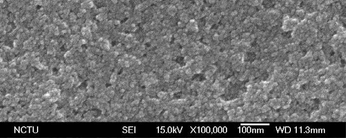
3 4.2 SEM AND OPTICAL ABSORPTION / EMISSION SPECTRA The overall layout figure of CMOS sensing chip is shown in Fig The most significant characteristic of the layout design is the electrodes structure combined with CMOS sensing circuits on the same silicon substrate. The electrodes structures are fabricated by opening a passivation window (86 μm * 86 μm) over two closely separated metal lines, as shown in Fig The electrodes are placed at the center part of the silicon chip for convenient nanodevice construction. The SEM image of the 13 electrodes and their sizes (width * length of oxide region between electrodes) are shown in Fig The electrodes, (1)-(8) are connected to the eight identical CMOS sensing circuits. The rest five electrodes, E1~E5 are connected directly to pads for direct measurement. The SEM images of the surface of SiO 2 /Si wafer fragments after repeated assembly process are shown in Fig. 4.7 (Au / AET-CdSe/ZnS nanostructure) and Fig. 4.8 (MSA-CdSe/ZnS / AET-CdSe/ZnS nanostructure). As we can see in the images, the structure become more and more compact when increases the number of layers step by step. Besides, for Au / AET-CdSe/ZnS nanostructure, after the multi-layered structure was formed, typically more than 3 layers, the gold color shining can be easily observed by naked eye. The fabrication process of the photo-sensing nanodevice on CMOS sensing chip is similar to that on SiO2/Si wafer fragments, as described in section 3.3. First, the silicon chip is modified by N-[3-(trimethoxysilyl)propyl]-ethylene diamine (TMSPED), which provides positive-charged amino (-NH3 + ) groups to attract negative (-COO - ) charged Au or MSA-CdSe/ZnS NPs. Second, the AET-modified CdSe/ZnS NPs that have positive-charged amino groups on the particle surface are assembled on Au or MSA-CdSe/ZnS NPs. Theoretically, the assembly process can be repeated for several times to form multi-layered nanostructure of CdSe/ZnS and/or Au NPs. Third, fixing the nanodevice-modified silicon chip on PCB by using aqueous insulation gel. In this step, the quick-drying gel with organic solvent is not suitable. Fourth, bonding wire from silicon chip to PCB, and 125 heating process is extremely 53
4 harmful to nanodevice during bonding. Fifth, measurement of nanodevice which fixing on PCB and then illumination the silicon chip by 2.5mW / cm 2 laser diodes (375 nm, 400 nm, 435 nm) under vacuum or normal room condition. Finally, remove the silicon chip from PCB and then SEM observation of nanodevice structure. The overall experimental procedure of fabrication and measurement of the photo-sensing nanodevices on TSMC 0.35 μm silicon chip is shown in Fig 4.9. The fabrication process of the photo-sensing nanodevices on silicon oxide substrate of TSMC 0.35 μm silicon chip was also observed by SEM, as shown in Fig (blank electrodes), Fig 4.11 (Au / AET-CdSe/ZnS nanostructure) and Fig 4.12 (MSA-CdSe/ZnS / AET-CdSe/ZnS nanostructure). From the SEM images, Fig and Fig. 4.12, it is interesting to note that, in additional to the silicon oxide surface, the surface of Al electrodes was also labeled with NPs. This phenomenon may be caused by the presence of the OH groups on the surface of the electrodes, which can be modified by TMSPED molecules, making them suitable sites for NP assembly. The presence of NPs on the Al electrodes enhances continuity at the interface between the NP s packed silicon oxide surface and the Al electrodes. Identically, it also enhances continuity at the interface between the NP s packed field oxide surface and the Al electrodes. Fig. 4.13(a) shows the cross section figure of the electrodes structure correspond to SEM image of the nanodevice-modified silicon chip. In theoretically, the NPs will be self-assembly covering the silicon chip. Although we cannot sure the edge between the Al electrodes and silicon oxide will be continuing self-assembly labeled with NPs firmly. In the worse case, we must consider the whole chip area (1460 μm * 1460 μm) for calculation, not the area of the electrodes. Fig. 4.13(b) shows the current flow trend of the nanodevice structure. Although it is very complicated for calculation, but we can sure that the electrodes dominated the source of the generated current. Furthermore, in order to prove that the closely packed nanostructure has superior optical properties, we used quartz glass to simulate the silicon oxide substrate and observed the variation of UV-visible and Photoluminescence (PL) intensity spectra at different layer nanostructure. From the absorption spectrum, we can see the peak of absorbance rises when the number of layers increases, 54
5 as shown in Fig Besides, the nanostructure retains the optical characteristics of CdSe/ZnS NPs when they are bound to each other, which can be verified by identifying the characteristic absorbance peaks of Au NPs (~520 nm) and CdSe/ZnS NPs (~580 nm) in the spectrum. However, in some cases, we observed the peaks of Au NPs (~520 nm) and CdSe/ZnS NPs (~580 nm) are so close that they merge to form a board band in the spectrum for Au / AET-CdSe/ZnS nanostructure as shown in Fig. 4.14(a). Specifically, both the absorption onset and the band edge peak of the CdSe/ZnS NPs are unaffected as a result of their binding to the Au NPs. By comparing the UV-visible spectrum to the sizing curve reported by Peng and co-workers [26], we obtained that the diameter of CdSe/ZnS NPs is about 4 nm ~ 5 nm, which can also be proved by TEM images. The PL intensity spectrum of multi-layered nanostructure on quartz glass was shown in Fig There are some important characteristics: First, the band edge peak of the PL intensity will increase in magnitude when the wavelength of incident light decreases (435 nm, 400 nm, 375 nm, 365 nm) [Fig. 4.15(a) and 4.15(c)]. It shows that more electron-hole-pairs are generated and return to the ground state under illumination with smaller excitation wavelength. Second, for both Au / AET-CdSe/ZnS and MSA-CdSe/ZnS / AET-CdSe/ZnS multi-layered structures, the PL intensity will also increase when the number of layers increases when we used 375 nm wavelength for optical excitation, as shown in Fig (b) and (d). It means that the nanostructure becomes more compact and has fewer defects on the particle surface. During the dip-and-wash procedure, the instable bond between the NPs will cause the existence of defect. So the probability of defect will be reduced when the number of layers increases. Third, as shown in Fig. 4.15(b), there is no absorption for Au NPs under optical excitation; therefore, there is no PL intensity with only a layer of Au NPs on quartz glass (Black Line). The PL intensity in 3-layered (5-layered) nanostructure is smaller than 2-layered (4-layered) nanostructure can also be proved. The Au NPs, which have no absorbance, block the incident light for CdSe/ZnS NPs to be photo-activated in the 3-layered (5-layered) structure. Fourth, we observed the PL intensity in 4-layered nanostructure become larger than 2-layered nanostructure. Specifically, they have the same structure that the CdSe/ZnS NPs was on 55
6 the top-layer. This result means that multi-layers constitute a more compact and fewer defects structure. The same, the 8-layered and 12-layered nanostructures show higher PL intensity than the 4-layered nanostructure. Nevertheless, although the ionic assembly using this dip-and-wash process can repeat as many times as we design to, the PL intensity increment will eventually be saturated. 4.3 Au / AET-CdSe/ZnS NANODEVICE In this section, we measured the I-V characteristics of multi-layered Au / AET-CdSe/ZnS nanodevice structure. The two electrodes sets we used, 30 μm / 15 μm and 30 μm / 5 μm (width / length) were directly connected to the bonding pads around the chip. After the fabrication process described in Section 3.3, the I-V measurement was performed by applying voltage biases to the electrodes and measuring the current flowing through the nanodevice while in dark or under illumination of 375 nm, 400 nm, 435 nm laser diode. The SEM pictures of the electrodes are in Fig Electrodes 1 and 2 have silicon oxide region of 30 μm * 15 μm and 30 μm * 5 μm (width * length) respectively. The measurement results of the nanodevice with the two sets of electrodes are shown in Fig If there is only one layer of Au NPs labeling between electrodes, as shown in Fig. 4.11(a), the I-V characteristics were virtually identical to those of blank electrodes. The current less than 10 fa was observed throughout the applied voltages (-1mV ~ 1mV) with or without illumination. The relatively large spacing between the Au NPs prohibited the electrons from tunneling. However, for multi-layered Au / AET-CdSe/ZnS nanodevice, we found that the nanodevice was resistive in dark and produced an obvious constant increment of photocurrent under illumination. Simultaneously, it was seen that the I-V curve passes through the second quadrant and hence the nanodevice can deliver power. In the previous work as described in section 2.2, for the 4-layered nanodevice composed of Citrate-capped Au NPs and Tyramine-capped CdSe NPs, there was constantly 1.2 na (30 μm / 5 μm) and 2 na (30 μm / 15 μm) increment of photocurrent throughout the applied voltage biases after
7 nm laser source illumination. In this present work, instead of using Tyramine-capped CdSe NP, we used AET-capped CdSe/ZnS NPs to construct the nanodevice. Basically the ZnS layer served as a passivation layer, which can make the particle structure stable. Besides the large band gap of ZnS contributed to higher quantum yield as we proposed in section 3.2. The measurement results of 4-layered nanodevice composed of Citrate-capped Au NPs and AET-capped CdSe/ZnS NPs show that there were constantly 28 na (30 μm / 5 μm) and 70 na (30 μm / 15 μm) increment of photocurrent throughout the applied voltage biases after 375 nm laser illumination. Even at zero bias point, this constant increment remained. So this confirms the higher performance by using AET-capped CdSe/ZnS NPs than Tyramine-capped CdSe NPs. Furthermore, for the measurement result of 12-layered nanodevice, there was constantly 56 na (30 μm / 5 μm) and 121 na (30 μm / 15 μm) increment of photocurrent throughout the applied voltage biases after illumination with 375 nm laser, and it had average R = 1.44 kω, V oc = mV (30 μm / 5 μm) and average R = 2.23 kω, V oc = mV (30 μm / 15 μm). There was more photocurrent generated as we used the electrodes of larger length, because there were more nano-schottky-diodes formed in the multi-layered structure between the electrodes. As we know that in previous work, the photocurrent volume density (PVD) (A/nm 3 ) of the nanodevice composed of Citrated-capped Au NPs and Tyramine-capped CdSe NPs, 4-layered nanodevice, is at least 38 times better than that of CdSe thin film [22]. In this work, we also compared the PVD of the Au / AET-CdSe/ZnS nanodevice with that of the CdSe thin film once more. We found that the PVD of the 4-layered nanodevice and 12-layered nanodevice composed of Au and AET-CdSe/ZnS NPs is at least 1183 and 682 times better than that of CdSe thin film, respectively. In sum, short-circuit current (I sc ), open-circuit voltage (V oc ), and PVD ratio of the 4, 8, 12-layered nanodevice structures under 375, 400, 435 nm wavelength illumination were shown in Table 4.1. In conclusion, there are several notable characteristics of the results in Fig and Table 4.1. First, the longer length of the electrodes leads to the larger photocurrent and larger V oc after illumination, because there was more nano-schottky-diodes formed in the structure and the length of 57
8 the electrodes depends on the equivalent resistance, therefore dominating the V oc. We obtained the same phenomenon as we used HSPICE to simulate two-dimension nano-schottky-diode"arrays model. The simulation condition is similar to the one-dimension diode-resistor arrays model described in section 2.2, except the resistance R1 changed to 0.25MΩ and one-dimensional diode-resistor array changed to two-dimensional one, as shown in Fig To simulate the nanodevice structure with long (short) length, 45 (15) stages were connected in series. The simulation results are shown in Table. 4.2, and we can observe the data just match the measurement results that the larger length of the electrodes (45 stages) leads to the larger photocurrent. Second, more photocurrent generated in shorter wavelength illumination because more electron-hole-pairs generated within the depletion region with uniform photoexcitation (hv > E g ). This result just matches the UV-visible and PL intensity spectra as shown in Fig and Fig. 4.15, respectively. Third, more photocurrent was generated in the nanostructure which has a larger number of layers. Fourth, from the Table 4.1, we found that the PVD ratio will gradually decrease when the number of layers increases. The PVD ratio means the PVD of the nanodevice compared with the CdSe thin film [22]. Theoretically, the photocurrent is proportioned to the PL intensity of the nanostructure; therefore, the photocurrent per unit volume (PVD) is proportional to the PL intensity per unit volume. From the PL intensity spectrum in the multi-layered Au / AET-CdSe/ZnS nanostructure, we found that the PL intensity did not increase as fast as the volume did; therefore we can confirm that the PVD ratio will decrease when the number of layers, that is the volume, increases. This phenomenon can also be observed from the HSPICE simulation results. Physically, when the number of layers increased, more nano-schottky-diodes were formed and therefore more photocurrent was generated. However, the increase of photocurrent does not mean that the efficiency will also increase proportionally, because the more layers the nanostructure has, the more nano-shottky-diodes are blocked from photo-excitation by the Au NPs in the upper layers. 58
9 4.4 MSA-CdSe/ZnS / AET-CdSe/ZnS NANODEVICE For the MSA-CdSe/ZnS / AET-CdSe/ZnS nanodevice with only a layer of MSA-CdSe/ZnS NPs on the silicon oxide substrate [Fig. 4.12(a)], the I-V characteristics was large resistive about 20GΩ (30 μm / 5 μm) and 60GΩ (30 μm / 15 μm) in dark and the photocurrent was less than 20 pa with 375 nm illumination. The measurement results of multi-layered nanodevice composed of MSA-CdSe/ZnS and AET-CdSe/ZnS NPs are shown in Fig For 12-layered nanodevice, there were 2.2 na (30 μm / 5 μm) and 3.1 na (30 μm / 15 μm) increment of photocurrent at zero bias (short-circuit current I sc ) after 375 nm illumination. In dark condition, the I-V characteristics was resistive about 0.88 GΩ (30 μm / 5 μm) and 0.99GΩ (30 μm / 15 μm). Although the electric resistance is not linearly proportional to the length of the electrodes (maybe due to the defects between CdSe/ZnS NPs), but we can make sure that the larger length of electrodes leads to the larger electric resistance in dark condition. Based on the results presented in Fig. 4.19, we can concluded that the nanodevice composed of only CdSe/ZnS NPs acts like a photoresistor whose resistance decreases with increasing incident light intensity. As described in literature, a photoresistor is made of a high-resistance semiconductor. If light illuminated on the device is of high enough frequency, photons absorbed by the semiconductor give bound electrons enough energy to jump into the conduction band. The resulting free electron (and its hole partner) conduct electricity, thereby lowering resistance. The only difference between the CdSe/ZnS nanodevice and conventional photoresistor is that the resistance decreased with decreasing incident light wavelength. In other words, shorter incident light wavelength caused more PL intensity as shown in Fig. 4.15(c). We also measured the different layered MSA-CdSe/ZnS / AET-CdSe/ZnS nanodevices with or without illumination, and the measurement results are shown in Table 4.3. At last, we found that the PVD of the 12-layered MSA-CdSe/ZnS / AET-CdSe/ZnS nanodevice is at least 34 times better than that of CdSe thin film [22]. In conclusion, there are several notable characteristics of the results in Fig. 4.19, and Table
10 First, unlike the I-V measurement results of the nanodevice composed of Au / AET-CdSe/ZnS NPs in which the conductivity remained constant with or without illumination, the conductivity of the nanodevice composed of MSA-CdSe/ZnS / AET-CdSe/ZnS NPs increased under illumination. In the Au / AET-CdSe/ZnS nanodevice, there are enormous number of nano-schottky-diodes in the structure which can absorb the illuminated light, generate electron-hole pairs in the depletion region and thus produce the photocurrent without changing the conductivity. In contrast, in MSA-CdSe/ZnS / AET-CdSe/ZnS nanodevice, there is no diode structure, only the same semiconductor material, CdSe/ZnS. When illuminated with light, the nanodevice can generate electron-hole-pairs, which in turn increase the conductivity. However, without the depletion region, the nanodevice can hardly produce photocurrent at zero bias. Therefore, we can conclude that the Au / AET-CdSe/ZnS nanodevice acts like a photodiode while the MSA-CdSe/ZnS / AET-CdSe/ZnS nanodevice acts like a photoresistor. Second, the longer length of electrodes leads to smaller electric resistance after illumination, which can be easily understood that the longer length the electrodes has, the more electron-hole-pairs generated after illumination. Third, from the Table 4.3, we found that the PVD ratio will increase when the number of layers increases. From the PL intensity spectra in the multi-layered MSA-CdSe/ZnS / AET-CdSe/ZnS nanostructure, we found that the growth rate of the PL intensity was larger than the growth rate of the volume; therefore we can confirm that the PVD ratio will increase when the number of layers increases. 4.5 Au / AET-CdSe/ZnS SOLOR CELL EFFICIENCY Solar cell is a critical technology for overcoming global environmental and energy problems. The invention of p-n junction in 1949 formed the basis of the discovery of the crystalline Si solar cell by Pearson in Since then, solar cells have been developed and produced with polysilicon, CdTe, and GaAs. Applications of solar cells are now an important and integral part of our daily lives, ranging from calculators to solar powered irrigation systems. Over 95% of solar cells in production 60
11 are silicon based. In our works, the nanodevice composed of Au and AET-CdSe/ZnS NPs has ultra-high performance of photo-sensing ability, as described in section 4.3. In order to show that the proposed nanodevice structure composed of NPs has a similar or even better photo-sensing ability than conventional solar cells, we calculate the power conversion efficiency and compare it with other solar cell structures. In the measurement results, we obtained the highest output power occurred in 8-layered nanodevice. The I-V characteristics of a solar cell were shown in Fig V oc is the maximum voltage obtainable at the load under open-circuit condition of the nanodevice, and I sc is the maximum current through the load under short-circuit condition. The power delivered by the nanodevice can be maximized by maximizing the area under the curve in Fig. 4.20, that is, maximizing the product (I sc * V oc ). By properly choosing the load resistor, the output power can be as high as (I m * V m ) = 0.8 * (I sc * V oc ) in typical p-n junction solar cell. In our system, the output power can be as high as (I m * V m ) = 0.5 * (I sc * V oc ). If we focus on 8-layered nanodevice which under 375 nm illumination, and then obtained the V oc -0.2mV (30 μm / 5 μm) and V oc -0.6mV (30 μm / 15 μm). From the result we can know that the V oc depended on the length of the electrodes and approximated to direct proportion to the length of the electrodes. As we know that the power efficiency is defined as J sc (ma / cm 2 ) * V oc / P in (mw / cm 2 ), so we must correct V oc when the electrodes area become more larger by extend the length of the electrodes. First, we set the length of the electrodes as an variable X, so the cell area was [ X] μm 2, and the image of the electrodes of size 30 μm / X μm (width / length) is shown in Fig The cell area was 2400 μm 2 (length X = 5 μm), and the short-circuit current I sc = 40 na as we measured. When the cell area is similar to 1cm 2, the length of the electrodes X = 1250,000 μm, and the J sc = 40 na / (1460 μm * 1460 μm) = 1.877*10-3 (ma / cm 2 ). However, the V oc ( X = 1250,000 μm) = -0.2mV ( X = 5 μm) 1250,000 / 5 = -50V. So the power efficiency = *10-3 ma 50V / 2.5mW = 1.89%. We also obtained the power efficiency can achieve 40% (X = 26625,000 μm) which larger than other solar cell structures before a 2005 technology overview [18]. Although such estimate method is not very accurate, because we can not make sure that such photocurrent can be generated when the 61
12 length of the electrodes become more large. In our future works, the nanodevice with large area electrodes will be designed and fabricated to verify our ideal inference. 4.6 THE PHOTO-SENSING CIRCUIT The measurement results of 4-layered, 30 μm * 5 μm electrodes, Au / AET-CdSe/ZnS nanodevice combined with CMOS sensing circuit was shown in Fig The measurement condition for measuring was shown in Table 4.4. The equivalent resistance of the nanodevice R d is about 7.5 kω. We fixed the V bias ~ V to make the dark current was first set closely to 50 na in both HSPICE simulation and this measurement, consequently, illuminated with different wavelengths (375, 400, 435 nm) of a 2.5mW / cm 2 laser source. The result of output versus I d in both HSPICE simulation and this measurement is also shown in Fig There are some notable characteristics of the result. First, the value of V ip is very close to V in = 1.7 V, which means the gain of negative feedback loop is large enough to lock V ip with V in. Second, the conductivity of the nanodevice is not increasing after light illumination, but the current flowing the nanodevice, I d, is increasing after light illumination. This phenomenon means the large number of reverse-biased Schottky diodes that had forward photovoltaic voltages to effectively increase the bias voltage across the nanodevice after light illumination and thus increase the current flowing the nanodevice. 62

 Source Meter Keithley 2410,")

13 375 nm, 400 nm, 435 nm Laser diode PicoQuant LDH-P-C375, 400, 435 Laser diode driver PicoQuant POL 800D (2.5mW / cm 2 ) Source Meter Keithley 2410, 1100V Vacuum chamber (Not necessary) Fig. 4.1 The environment setup for I-V characteristics measurement. 63
14 Fig. 4.2 The environment setup for UV-visible absorbance spectrum measurement. 375 nm, 400 nm, 435 nm photo-excitation Filter out < 500 nm Fig. 4.3 The environment setup for PL intensity spectrum measurement. 64

15 Electrodes of different size CMOS sensing circuit Fig. 4.4 The layout of the CMOS sensing chip. The chip is 1460 μm * 1460 μm and has 48 pins. There are eight identical CMOS sensing circuits at the corner part of the chip, and thirteen different size/shape electrodes at the center part of the chip. 65
 are connected by vias.")
16 Fig. 4.5 The cross section figure of electrodes structure, where the four layers of metal lines (~ 6 μm thickness) are connected by vias. The passivation window in this work is 86 μm * 86 μm. The silicon oxide region between Al electrodes has different shapes. 66
~(8), are connected to the eight identical CMOS sensing circuits.")
17 (a) (b) Fig. 4.6 (a) The SEM image of the 13 electrodes. (b) The size (width * length between electrodes) figure of the corresponding 13 electrodes. The electrodes, (1)~(8), are connected to the eight identical CMOS sensing circuits. The rest five electrodes, E1~E5 are connected directly to pads for direct measurement. 67


18 (a) Au NPs on SiO2/Si wafer fragment (b) AET-CdSe/ZnS NPs + Au NPs on SiO2/Si wafer fragment 68

")


19 (c) Au NPs + AET-CdSe/ZnS NPs + Au NPs on SiO2/Si wafer fragment (d) AET-CdSe/ZnS NPs + Au NPs + AET-CdSe/ZnS NPs + Au NPs on SiO2/Si wafer fragment 69


20 (e) Au NPs + AET-CdSe/ZnS NPs + Au NPs + AET-CdSe/ZnS NPs + Au NPs on SiO2/Si wafer fragment Fig. 4.7 The SEM images (100k magnification) of Au / AET-CdSe/ZnS nanostructure of different level construction are shown above (a)~(e). 70


21 (a) MSA-CdSe/ZnS NPs on SiO2/Si wafer fragment (b) AET-CdSe/ZnS NPs + MSA-CdSe/ZnS NPs on SiO2/Si wafer fragment 71


22 (c) MSA-CdSe/ZnS + AET-CdSe/ZnS NPs + MSA-CdSe/ZnS NPs on SiO2/Si wafer fragment (d) AET-CdSe/ZnS NPs + MSA-CdSe/ZnS + AET-CdSe/ZnS NPs + MSA-CdSe/ZnS NPs on SiO2/Si wafer fragment 72


23 (e) MSA-CdSe/ZnS + AET-CdSe/ZnS NPs + MSA-CdSe/ZnS + AET-CdSe/ZnS NPs + MSA-CdSe/ZnS NPs on SiO2/Si wafer fragment Fig. 4.8 The SEM images (100k magnification) of MSA-CdSe/ZnS / AET-CdSe/ZnS nanostructure of different level construction are shown above (a)~(e). 73
24 Fig. 4.9 The overall experimental procedure of fabrication and measurement of photo-sensing nanodevice on TSMC 0.35 μm silicon chip. 74


25 (a) (b) 75
 30 μm * 5 μm electrodes (950 magnification), (b) 30 μm * 15")
26 (c) Fig The SEM images of blank electrodes (a) 30 μm * 5 μm electrodes (950 magnification), (b) 30 μm * 15 μm electrodes (950 magnification), (c) The edge part of the electrodes (50k magnification). 76


27 (a) (b) 77


 1-layered nanostructure,")
 8-layered nanostructure,")
28 (c) (d) Fig The SEM images (70k magnification) of the edge part of Au / AET-CdSe/ZnS NPs modified electrodes. (a) 1-layered nanostructure, (b) 4-layered nanostructure, (c) 8-layered nanostructure, (d) 12-layered nanostructure. 78


29 (a) (b) 79


 4-layered nanostructure,")
30 (c) (d) Fig The SEM images (70k magnification) of the edge part of MSA-CdSe/ZnS / AET-CdSe/ZnS NPs modified electrodes. (a) 1-layered nanostructure, (b) 4-layered nanostructure, (c) 6-layered nanostructure, (d) 12-layered nanostructure. 80

31 (a) 81
32 (b) Fig (a) The cross section figure of the electrodes structure corresponds to SEM image of the nanodevice-modified silicon chip. (b) The current flow trend of the nanodevice structure, and the electrodes dominated the source of the generated current. In the worse case, we must consider the whole chip area for calculation, not the area of the electrodes. (The twill line means the thin film structure composed of NPs). 82
33 (a) (b) Fig The UV-visible absorption spectrum of multi-layered nanostructure on quartz glass. (a) Au / AET-CdSe/ZnS (b) MSA-CdSe/ZnS / AET-CdSe/ZnS. The Light Gray Line: 10% TMSPED/methanol ->quartz glass. The Black Line: 1-layered nanostructure. The Red Line: 2-layered nanostructure. The Green Line: 3-layered nanostructure. The Blue Line: 4-layered nanostructure. The Magenta Line: 5-layered nanostructure. 83
34 (a) (b) 84
35 (c) (d) 85

36 Fig The PL emission spectrum of multi-layered nanostructures on quartz glass. (a)(c) The PL intensity of Au / AET-CdSe/ZnS and MSA-CdSe/ZnS / AET-CdSe/ZnS, 4-layered nanostructure. The Red Line: photo-excitation with 435nm wavelength; The Green Line: photo-excitation with 400 nm wavelength; The Blue Line: photo-excitation with 375 nm wavelength; The Black Line: photo-excitation with 365 nm wavelength. (b)(d) The PL intensity of Au / AET-CdSe/ZnS and MSA-CdSe/ZnS / AET-CdSe/ZnS, multi-layered nanostructure under 375 nm photo-excitation. The Black Line: 1-layered nanostructure; The Red Line: 2-layered nanostructure; The Green Line: 3-layered nanostructure; The Blue Line: 4-layered nanostructure; The Magenta Line: 5-layered nanostructure; The Yellow Line: 8-layered (b) and 6-layered (d) nanostructure; The Orange Line: 12-layered nanostructure. Electrodes 1 Electrodes 2 Fig The electrodes under measuring are shown above. Electrodes 1 and 2 have silicon oxide region of 30 μm * 15 μm and 30 μm * 5 μm (width * length), respectively. 86
37 AET-CdSe/ZnS / Au / AET-CdSe/ZnS / Au / SiO 2 4-layered, 30 μm * 5 μm electrodes AET-CdSe/ZnS / Au / AET-CdSe/ZnS / Au / SiO 2 4-layered, 30 μm * 15 μm electrodes 87
38 AET-CdSe/ZnS / Au / AET-CdSe/ZnS / Au / AET-CdSe/ZnS / Au / AET-CdSe/ZnS / Au / SiO 2 8-layered, 30 μm * 5 μm electrodes AET-CdSe/ZnS / Au / AET-CdSe/ZnS / Au / AET-CdSe/ZnS / Au / AET-CdSe/ZnS / Au / SiO 2 8-layered, 30 μm * 15 μm electrodes 88
39 AET-CdSe/ZnS / Au / AET-CdSe/ZnS / Au / AET-CdSe/ZnS / Au / AET-CdSe/ZnS / Au / AET-CdSe/ZnS / Au / AET-CdSe/ZnS / Au / SiO 2 12-layered, 30 μm * 5 μm electrodes AET-CdSe/ZnS / Au / AET-CdSe/ZnS / Au / AET-CdSe/ZnS / Au / AET-CdSe/ZnS / Au / AET-CdSe/ZnS / Au / AET-CdSe/ZnS / Au / SiO 2 12-layered, 30 μm * 15 μm electrodes Fig The I-V curves of the multi-layered Au / AET-CdSe/ZnS photo-sensing nanodevice when in dark (black line) or illumination with 375 nm (blue line), 400 nm (green line), 435 nm (red line) laser diode. 89
40 Req Isc Voc PVD Ratio (375 nm) Isc Voc PVD Ratio (400 nm) Isc Voc PVD Ratio (435 nm) 30μm * 5μm Electrodes 30μm * 15μm Electrodes 4-layered 7.2KΩ 8-layered 4.8KΩ 12-layered 1.44KΩ 4-layered 11.4KΩ 28nA 40nA 56nA 70nA mV mV mV mV nA 30nA 40nA 42nA mV mV mV -0.48mV nA 20nA 27nA 29nA mV mV mV mV layered 6.9KΩ 12-layered 2.23KΩ 93nA 121nA mV -0.27mV nA 94nA -0.49mV -0.21mV nA 74nA -0.38mV mV Table. 4.1 The measurement results of short-circuit current I sc, open-circuit voltage V oc, and photocurrent volume dendity (PVD) ratio of Au / AET-CdSe/ZnS, multi-layered nanodevice. 90

41 (a) (b) 91
42 (c) Fig (a) Two-dimensional array of resistors and nano-schottky-diodes. (b) (c) The models for nanodevice in dark and under illumination. For HSPICE simulation, Metal-Insulator-Semiconductor diode model was employed, V = 0.4 V, R1 = 0.25 MΩ, R2 = 5 MΩ and I = 5 pa. 4-layered nanostructure I dark I illumination I ph 30 μm * 5 μm (15 stages) 6.38 pa 9.62 pa 3.24 pa 30 μm * 15 μm (45 stages) 0.53 pa 6.95 pa 6.42 pa 8-layered nanostructure I dark I illumination I ph 30 μm * 5 μm (15 stages) 9.63 pa pa 6.23 pa 30 μm * 15 μm (45 stages) 0.95 pa pa pa 12-layered nanostructure I dark I illumination I ph 30 μm * 5 μm (15 stages) pa pa 8.84 pa 30 μm * 15 μm (45 stages) 1.26 pa pa 15.9 pa Table. 4.2 The simulation results of multi-layers, two-dimensional nano-schottky-diode arrays model by using HSPICE software. 92
43 MSA-CdSe/ZnS / SiO 2 1-layered, 30 μm * 5 μm electrodes MSA-CdSe/ZnS / SiO 2 1-layered, 30 μm * 15 μm electrodes 93
44 AET-CdSe/ZnS / MSA-CdSe/ZnS / AET-CdSe/ZnS / MSA-CdSe/ZnS / SiO 2 4-layered, 30 μm * 5 μm electrodes AET-CdSe/ZnS / MSA-CdSe/ZnS / AET-CdSe/ZnS / MSA-CdSe/ZnS / SiO 2 4-layered, 30 μm * 15 μm electrodes 94
45 AET-CdSe/ZnS / MSA-CdSe/ZnS / AET-CdSe/ZnS / MSA-CdSe/ZnS / AET-CdSe/ZnS / MSA-CdSe/ZnS / SiO 2 6-layered, 30 μm * 5 μm electrodes AET-CdSe/ZnS / MSA-CdSe/ZnS / AET-CdSe/ZnS / MSA-CdSe/ZnS / AET-CdSe/ZnS / MSA-CdSe/ZnS / SiO 2 6-layered, 30 μm * 15 μm electrodes 95
46 AET-CdSe/ZnS / MSA-CdSe/ZnS / AET-CdSe/ZnS / MSA-CdSe/ZnS / AET-CdSe/ZnS / MSA-CdSe/ZnS / AET-CdSe/ZnS / MSA-CdSe/ZnS / AET-CdSe/ZnS / MSA-CdSe/ZnS / AET-CdSe/ZnS / MSA-CdSe/ZnS / SiO 2 12-layered, 30 μm * 5 μm electrodes AET-CdSe/ZnS / MSA-CdSe/ZnS / AET-CdSe/ZnS / MSA-CdSe/ZnS / AET-CdSe/ZnS / MSA-CdSe/ZnS / AET-CdSe/ZnS / MSA-CdSe/ZnS / AET-CdSe/ZnS / MSA-CdSe/ZnS / AET-CdSe/ZnS / MSA-CdSe/ZnS / SiO 2 12-layered, 30 μm * 15 μm electrodes 96
47 Fig The I-V curves of the multi-layered MSA-CdSe/Zn / AET-CdSe/ZnS photo-sensing nanodevice when in dark (black line) or illumination with 375 nm (blue line), 400 nm (green line), 435 nm (red line) laser diode. Isc PVD Ratio (375 nm) 30μm * 5μm Electrodes 30μm * 15μm Electrodes 4-layered 6-layered 12-layered 4-layered 6-layered 12-layered 0.4nA 0.7nA 2.2nA 0.7nA 1.2nA 3.1nA Isc 0.3nA 0.6nA 1.7nA 0.5nA 1nA 2.3nA PVD Ratio (400 nm) Isc 0.2nA 0.5nA 1.3nA 0.3nA 0.7nA 1.9nA PVD Ratio (435 nm) Table. 4.3 The measurement results of short-circuit current I sc, and photocurrent volume dendity (PVD) ratio of MSA-CdSe/ZnS / AET-CdSe/ZnS, multi-layered nanodevice. 97
48 (a) (b) Fig I-V characteristics of an illuminated solar cell. (a) Typical p-n junction solar cell in the fourth quadrant. (b) Au / AET-CdSe/ZnS solar cell in the second quadrant. 98
 375 nm,400 nm,435 nm Table. 4.4 The measurement conditions for measure the Au / AET-CdSe/ZnS, 4-layered nanodevice, 30μm * 5μm electrodes combined with CMOS sensing circuit.")
49 Fig The electrodes of size 30 μm / X μm (width / length) Vdd 3.3 V Vop 2 V Vin 1.7 V Vbias ~ V Ioffset 6 μa Reset Square wave, 3~0 V, 500 khz Rd ~ 7.5 kω Laser source (2.5mW / cm 2 ) 375 nm,400 nm,435 nm Table. 4.4 The measurement conditions for measure the Au / AET-CdSe/ZnS, 4-layered nanodevice, 30μm * 5μm electrodes combined with CMOS sensing circuit. 99
50 (a) In dark condition, I d ~ 50 na, Output = 1.54 V (b) Under 435 nm illumination, I d ~ 63 na, Output = 1.98 V 100
51 (c) Under 400 nm illumination, I d ~ 72 na, Output = 2.3 V (d) Under 375 nm illumination, I d ~ 81 na, Output = 2.58 V Fig The measurement results of 4-layered, 30μm * 5μm electrodes, Au / AET-CdSe/ZnS nanodevice combined with CMOS sensing circuit are shown above (a)~(d), where I d means the current following through the R d ~ 7.5kΩ. In this measurement, we fixed the V bias ~ V and then illuminated with laser source or under dark condition. 101
52 Fig The result of output versus I d in both HSPICE simulation (dark line) and this measurement of photo-sensing circuit (red line). The power intensity of the laser diodes (375, 400, 435 nm) is 2.5mW / cm
CHAPTER 3. FABRICATION TECHNOLOGIES OF CdSe/ZnS / Au NANOPARTICLES AND NANODEVICES. 3.1 THE SYNTHESIS OF Citrate-Capped Au NANOPARTICLES
 CHAPTER 3 FABRICATION TECHNOLOGIES OF CdSe/ZnS / Au NANOPARTICLES AND NANODEVICES 3.1 THE SYNTHESIS OF Citrate-Capped Au NANOPARTICLES Au NPs with ~ 15 nm were prepared by citrate reduction of HAuCl 4
OPTI510R: Photonics. Khanh Kieu College of Optical Sciences, University of Arizona Meinel building R.626
 OPTI510R: Photonics Khanh Kieu College of Optical Sciences, University of Arizona kkieu@optics.arizona.edu Meinel building R.626 Announcements Homework #6 is assigned, due May 1 st Final exam May 8, 10:30-12:30pm
Supplementary Figure 1 XRD pattern of a defective TiO 2 thin film deposited on an FTO/glass substrate, along with an XRD pattern of bare FTO/glass
 Supplementary Figure 1 XRD pattern of a defective TiO 2 thin film deposited on an FTO/glass substrate, along with an XRD pattern of bare FTO/glass and a reference pattern of anatase TiO 2 (JSPDS No.: 21-1272).
Understanding Semiconductor Lasers
 27 April 2010 age 1 of 8 Experiment II Understanding Semiconductor Lasers The purpose of this experiment is to explore the basic characteristics of semiconductor lasers. We will measure and calculate the
Supplementary Figures
 Supplementary Figures Supplementary Figure 1. AFM profiles of the charge transport and perovskite layers. AFM Image showing the thickness (y axis) of the layer with respect to the horizontal position of
Organic Electronic Devices
 Organic Electronic Devices Week 4: Organic Photovoltaic Devices Lecture 4.2: Characterizing Device Parameters in OPVs Bryan W. Boudouris Chemical Engineering Purdue University 1 Lecture Overview and Learning
EE 5344 Introduction to MEMS CHAPTER 5 Radiation Sensors
 EE 5344 Introduction to MEMS CHAPTER 5 Radiation Sensors 5. Radiation Microsensors Radiation µ-sensors convert incident radiant signals into standard electrical out put signals. Radiant Signals Classification
Supplementary Figure 3. Transmission spectrum of Glass/ITO substrate.
 Supplementary Figure 1. The AFM height and SKPM images of PET/Ag-mesh/PH1000 and PET/Ag-mesh/PH1000/PEDOT:PSS substrates. (a, e) AFM height images on the flat PET area. (c, g) AFM height images on Ag-mesh
KATIHAL FİZİĞİ MNT-510
 KATIHAL FİZİĞİ MNT-510 YARIİLETKENLER Kaynaklar: Katıhal Fiziği, Prof. Dr. Mustafa Dikici, Seçkin Yayıncılık Katıhal Fiziği, Şakir Aydoğan, Nobel Yayıncılık, Physics for Computer Science Students: With
Reference literature. (See: CHEM 2470 notes, Module 8 Textbook 6th ed., Chapters )
") September 17, 2018 Reference literature (See: CHEM 2470 notes, Module 8 Textbook 6th ed., Chapters 13-14 ) Reference.: https://slideplayer.com/slide/8354408/ Spectroscopy Usual Wavelength Type of Quantum
September 17, 2018 Reference literature (See: CHEM 2470 notes, Module 8 Textbook 6th ed., Chapters 13-14 ) Reference.: https://slideplayer.com/slide/8354408/ Spectroscopy Usual Wavelength Type of Quantum
Chapter 7. Solar Cell
 Chapter 7 Solar Cell 7.0 Introduction Solar cells are useful for both space and terrestrial application. Solar cells furnish the long duration power supply for satellites. It converts sunlight directly
Supporting Information s for
 Supporting Information s for # Self-assembling of DNA-templated Au Nanoparticles into Nanowires and their enhanced SERS and Catalytic Applications Subrata Kundu* and M. Jayachandran Electrochemical Materials
Compact Knowledge: Absorbance Spectrophotometry. Flexible. Reliable. Personal.
 L A B O R A T O R Y C O M P E T E N C E Compact Knowledge: Absorbance Spectrophotometry Flexible. Reliable. Personal. The interaction of light with molecules is an essential and well accepted technique
Supporting Information
 Electronic Supplementary Material (ESI) for Journal of Materials Chemistry A. This journal is The Royal Society of Chemistry 2018 Supporting Information A minimal non-radiative recombination loss for efficient
Spectroscopy. Page 1 of 8 L.Pillay (2012)
") Spectroscopy Electromagnetic radiation is widely used in analytical chemistry. The identification and quantification of samples using electromagnetic radiation (light) is called spectroscopy. Light has
Spectroscopy Electromagnetic radiation is widely used in analytical chemistry. The identification and quantification of samples using electromagnetic radiation (light) is called spectroscopy. Light has
EE 5611 Introduction to Microelectronic Technologies Fall Tuesday, September 23, 2014 Lecture 07
 EE 5611 Introduction to Microelectronic Technologies Fall 2014 Tuesday, September 23, 2014 Lecture 07 1 Introduction to Solar Cells Topics to be covered: Solar cells and sun light Review on semiconductor
ELECTRONIC DEVICES AND CIRCUITS SUMMARY
 ELECTRONIC DEVICES AND CIRCUITS SUMMARY Classification of Materials: Insulator: An insulator is a material that offers a very low level (or negligible) of conductivity when voltage is applied. Eg: Paper,
Conductivity and Semi-Conductors
 Conductivity and Semi-Conductors J = current density = I/A E = Electric field intensity = V/l where l is the distance between two points Metals: Semiconductors: Many Polymers and Glasses 1 Electrical Conduction
EE495/695 Introduction to Semiconductors I. Y. Baghzouz ECE Department UNLV
 EE495/695 Introduction to Semiconductors I Y. Baghzouz ECE Department UNLV Introduction Solar cells have always been aligned closely with other electronic devices. We will cover the basic aspects of semiconductor
Thermally Stable Silver Nanowires-embedding. Metal Oxide for Schottky Junction Solar Cells
 Supporting Information Thermally Stable Silver Nanowires-embedding Metal Oxide for Schottky Junction Solar Cells Hong-Sik Kim, 1 Malkeshkumar Patel, 1 Hyeong-Ho Park, Abhijit Ray, Chaehwan Jeong, # and
Designing Information Devices and Systems II A. Sahai, J. Roychowdhury, K. Pister Discussion 1A
 EECS 16B Spring 2019 Designing Information Devices and Systems II A. Sahai, J. Roychowdhury, K. Pister Discussion 1A 1 Semiconductor Physics Generally, semiconductors are crystalline solids bonded into
25 Instruments for Optical Spectrometry
 25 Instruments for Optical Spectrometry 25A INSTRUMENT COMPONENTS (1) source of radiant energy (2) wavelength selector (3) sample container (4) detector (5) signal processor and readout (a) (b) (c) Fig.
February 1, 2011 The University of Toledo, Department of Physics and Astronomy SSARE, PVIC
 FUNDAMENTAL PROPERTIES OF SOLAR CELLS February 1, 2011 The University of Toledo, Department of Physics and Astronomy SSARE, PVIC Principles and Varieties of Solar Energy (PHYS 4400) and Fundamentals of
Fall 2014 Nobby Kobayashi (Based on the notes by E.D.H Green and E.L Allen, SJSU) 1.0 Learning Objectives
 1.0 Learning Objectives") University of California at Santa Cruz Electrical Engineering Department EE-145L: Properties of Materials Laboratory Lab 7: Optical Absorption, Photoluminescence Fall 2014 Nobby Kobayashi (Based on the
University of California at Santa Cruz Electrical Engineering Department EE-145L: Properties of Materials Laboratory Lab 7: Optical Absorption, Photoluminescence Fall 2014 Nobby Kobayashi (Based on the
High-Performance Photocoupler Based on Perovskite Light Emitting Diode and Photodetector
 Supporting information for High-Performance Photocoupler Based on Perovskite Light Emitting Diode and Photodetector Zhi-Xiang Zhang, Ji-Song Yao, Lin Liang, Xiao-Wei Tong, Yi Lin, Feng-Xia Liang, *, Hong-Bin
Electrons are shared in covalent bonds between atoms of Si. A bound electron has the lowest energy state.
 Photovoltaics Basic Steps the generation of light-generated carriers; the collection of the light-generated carriers to generate a current; the generation of a large voltage across the solar cell; and
1 Name: Student number: DEPARTMENT OF PHYSICS AND PHYSICAL OCEANOGRAPHY MEMORIAL UNIVERSITY OF NEWFOUNDLAND. Fall :00-11:00
 1 Name: DEPARTMENT OF PHYSICS AND PHYSICAL OCEANOGRAPHY MEMORIAL UNIVERSITY OF NEWFOUNDLAND Final Exam Physics 3000 December 11, 2012 Fall 2012 9:00-11:00 INSTRUCTIONS: 1. Answer all seven (7) questions.
Supplementary Information. Back-Contacted Hybrid Organic-Inorganic Perovskite Solar Cells
 Electronic Supplementary Material (ESI) for Journal of Materials Chemistry C. This journal is The Royal Society of Chemistry 2016 Journal of Materials Chemistry C Supplementary Information Back-Contacted
Supplementary Figure 1. Supplementary Figure 1 Characterization of another locally gated PN junction based on boron
 Supplementary Figure 1 Supplementary Figure 1 Characterization of another locally gated PN junction based on boron nitride and few-layer black phosphorus (device S1). (a) Optical micrograph of device S1.
Photocurrent and Photovoltaic of Photodetector based on Porous Silicon
 Available online at www.worldscientificnews.com WSN 77(2) (217) 314-325 EISSN 2392-2192 Photocurrent and Photovoltaic of Photodetector based on Porous Silicon ABSTRACT Hasan A. Hadi Department of Physics,
Practical 1P4 Energy Levels and Band Gaps
 Practical 1P4 Energy Levels and Band Gaps What you should learn from this practical Science This practical illustrates some of the points from the lecture course on Elementary Quantum Mechanics and Bonding
3.1 Introduction to Semiconductors. Y. Baghzouz ECE Department UNLV
 3.1 Introduction to Semiconductors Y. Baghzouz ECE Department UNLV Introduction In this lecture, we will cover the basic aspects of semiconductor materials, and the physical mechanisms which are at the
Interdisciplinary Graduate School, Nanyang Technological University, Singapore , Singapore.
 Electronic Supplementary Material (ESI) for Nanoscale. This journalelectronic is TheSupplementary Royal Society Information of Chemistry (ESI) for 2014 Nanoscale. Triple-layer nanostructured WO 3 photoanodes
Supplementary Figure 1. Cross-section SEM image of the polymer scaffold perovskite film using MAI:PbI 2 =1:1 in DMF solvent on the FTO/glass
 Supplementary Figure 1. Cross-section SEM image of the polymer scaffold perovskite film using MAI:PbI 2 =1:1 in DMF solvent on the FTO/glass substrate. Scale bar: 1 m. Supplementary Figure 2. Contact angle
Design and Development of a Smartphone Based Visible Spectrophotometer for Analytical Applications
 Design and Development of a Smartphone Based Visible Spectrophotometer for Analytical Applications Bedanta Kr. Deka, D. Thakuria, H. Bora and S. Banerjee # Department of Physicis, B. Borooah College, Ulubari,
Practical 1P4 Energy Levels and Band Gaps
 Practical 1P4 Energy Levels and Band Gaps What you should learn from this practical Science This practical illustrates some of the points from the lecture course on Elementary Quantum Mechanics and Bonding
Electronic Supplementary Information for
 Electronic Supplementary Material (ESI) for Journal of Materials Chemistry C. This journal is The Royal Society of Chemistry 018 Electronic Supplementary Information for Broadband Photoresponse Based on
Electronic Supplementary Information
 Electronic Supplementary Information High Electrocatalytic Activity of Self-standing Hollow NiCo 2 S 4 Single Crystalline Nanorod Arrays towards Sulfide Redox Shuttles in Quantum Dot-sensitized Solar Cells
PHYSICS nd TERM Outline Notes (continued)
") PHYSICS 2800 2 nd TERM Outline Notes (continued) Section 6. Optical Properties (see also textbook, chapter 15) This section will be concerned with how electromagnetic radiation (visible light, in particular)
PHYSICS 2800 2 nd TERM Outline Notes (continued) Section 6. Optical Properties (see also textbook, chapter 15) This section will be concerned with how electromagnetic radiation (visible light, in particular)
Full-color Subwavelength Printing with Gapplasmonic
 Supporting information for Full-color Subwavelength Printing with Gapplasmonic Optical Antennas Masashi Miyata, Hideaki Hatada, and Junichi Takahara *,, Graduate School of Engineering, Osaka University,
SUPPLEMENTARY INFORMATION
 Supplementary Information: Photocurrent generation in semiconducting and metallic carbon nanotubes Maria Barkelid 1*, Val Zwiller 1 1 Kavli Institute of Nanoscience, Delft University of Technology, Delft,
Opto-electronic Characterization of Perovskite Thin Films & Solar Cells
 Opto-electronic Characterization of Perovskite Thin Films & Solar Cells Arman Mahboubi Soufiani Supervisors: Prof. Martin Green Prof. Gavin Conibeer Dr. Anita Ho-Baillie Dr. Murad Tayebjee 22 nd June 2017
Supporting Information
 Electronic Supplementary Material (ESI) for ChemComm. This journal is The Royal Society of Chemistry 2015 Supporting Information All inorganic cesium lead halide perovskite nanocrystals for photodetector
Supplementary Materials
 Supplementary Materials Sample characterization The presence of Si-QDs is established by Transmission Electron Microscopy (TEM), by which the average QD diameter of d QD 2.2 ± 0.5 nm has been determined
Electron Energy, E E = 0. Free electron. 3s Band 2p Band Overlapping energy bands. 3p 3s 2p 2s. 2s Band. Electrons. 1s ATOM SOLID.
 Electron Energy, E Free electron Vacuum level 3p 3s 2p 2s 2s Band 3s Band 2p Band Overlapping energy bands Electrons E = 0 1s ATOM 1s SOLID In a metal the various energy bands overlap to give a single
Supporting Information
 Supporting Information Oh et al. 10.1073/pnas.0811923106 SI Text Hysteresis of BPE-PTCDI MW-TFTs. Fig. S9 represents bidirectional transfer plots at V DS 100VinN 2 atmosphere for transistors constructed
A new concept of charging supercapacitors based on a photovoltaic effect
 Electronic Supplementary Material (ESI) for ChemComm. This journal is The Royal Society of Chemistry 2016 Electronic supporting information (ESI) A new concept of charging supercapacitors based on a photovoltaic
Single Photon detectors
 Single Photon detectors Outline Motivation for single photon detection Semiconductor; general knowledge and important background Photon detectors: internal and external photoeffect Properties of semiconductor
Flexible Organic Photovoltaics Employ laser produced metal nanoparticles into the absorption layer 1. An Introduction
 Flexible Organic Photovoltaics Employ laser produced metal nanoparticles into the absorption layer 1. An Introduction Among the renewable energy sources that are called to satisfy the continuously increased
Electronic Supplementary Information: Synthesis and Characterization of Photoelectrochemical and Photovoltaic Cu2BaSnS4 Thin Films and Solar Cells
 Electronic Supplementary Material (ESI) for Journal of Materials Chemistry C. This journal is The Royal Society of Chemistry 2017 Electronic Supplementary Information: Synthesis and Characterization of
Chapter 6 Photoluminescence Spectroscopy
 Chapter 6 Photoluminescence Spectroscopy Course Code: SSCP 4473 Course Name: Spectroscopy & Materials Analysis Sib Krishna Ghoshal (PhD) Advanced Optical Materials Research Group Physics Department, Faculty
TECHNICAL INFORMATION. Quantum Dot
 Quantum Dot Quantum Dot is the nano meter sized semiconductor crystal with specific optical properties originates from the phenomenon which can be explained by the quantum chemistry and quantum mechanics.
Because light behaves like a wave, we can describe it in one of two ways by its wavelength or by its frequency.
 Light We can use different terms to describe light: Color Wavelength Frequency Light is composed of electromagnetic waves that travel through some medium. The properties of the medium determine how light
3.1 Absorption and Transparency
 3.1 Absorption and Transparency 3.1.1 Optical Devices (definitions) 3.1.2 Photon and Semiconductor Interactions 3.1.3 Photon Intensity 3.1.4 Absorption 3.1 Absorption and Transparency Objective 1: Recall
= 6 (1/ nm) So what is probability of finding electron tunneled into a barrier 3 ev high?
 So what is probability of finding electron tunneled into a barrier 3 ev high?") STM STM With a scanning tunneling microscope, images of surfaces with atomic resolution can be readily obtained. An STM uses quantum tunneling of electrons to map the density of electrons on the surface
STM STM With a scanning tunneling microscope, images of surfaces with atomic resolution can be readily obtained. An STM uses quantum tunneling of electrons to map the density of electrons on the surface
Chemistry Instrumental Analysis Lecture 8. Chem 4631
 Chemistry 4631 Instrumental Analysis Lecture 8 UV to IR Components of Optical Basic components of spectroscopic instruments: stable source of radiant energy transparent container to hold sample device
Lecture 20 Optical Characterization 2
 Lecture 20 Optical Characterization 2 Schroder: Chapters 2, 7, 10 1/68 Announcements Homework 5/6: Is online now. Due Wednesday May 30th at 10:00am. I will return it the following Wednesday (6 th June).
Auger Electron Spectroscopy Overview
 Auger Electron Spectroscopy Overview Also known as: AES, Auger, SAM 1 Auger Electron Spectroscopy E KLL = E K - E L - E L AES Spectra of Cu EdN(E)/dE Auger Electron E N(E) x 5 E KLL Cu MNN Cu LMM E f E
Nanoelectronics. Topics
 Nanoelectronics Topics Moore s Law Inorganic nanoelectronic devices Resonant tunneling Quantum dots Single electron transistors Motivation for molecular electronics The review article Overview of Nanoelectronic
Self-study problems and questions Processing and Device Technology, FFF110/FYSD13
 Self-study problems and questions Processing and Device Technology, FFF110/FYSD13 Version 2016_01 In addition to the problems discussed at the seminars and at the lectures, you can use this set of problems
Photoelectric Effect Experiment
 Experiment 1 Purpose The photoelectric effect is a key experiment in modern physics. In this experiment light is used to excite electrons that (given sufficient energy) can escape from a material producing
Tailoring of Electron Collecting Oxide Nano-Particulate Layer for Flexible Perovskite Solar Cells. Gajeong-Ro, Yuseong-Gu, Daejeon , Korea
 Supporting Information Tailoring of Electron Collecting Oxide Nano-Particulate Layer for Flexible Perovskite Solar Cells Seong Sik Shin 1,2,, Woon Seok Yang 1,3,, Eun Joo Yeom 1,4, Seon Joo Lee 1, Nam
CBSE PHYSICS QUESTION PAPER (2005)
") CBSE PHYSICS QUESTION PAPER (2005) (i) (ii) All questions are compulsory. There are 30 questions in total. Questions 1 to 8 carry one mark each, Questions 9 to 18 carry two marks each, Question 19 to 27
CBSE PHYSICS QUESTION PAPER (2005) (i) (ii) All questions are compulsory. There are 30 questions in total. Questions 1 to 8 carry one mark each, Questions 9 to 18 carry two marks each, Question 19 to 27
ET3034TUx Utilization of band gap energy
 ET3034TUx - 3.3.1 - Utilization of band gap energy In the last two weeks we have discussed the working principle of a solar cell and the external parameters that define the performance of a solar cell.
Two-dimensional homologous perovskites as light absorbing materials for solar cell applications
 Supporting Information for Two-dimensional homologous perovskites as light absorbing materials for solar cell applications Duyen H. Cao, Constantinos C. Stoumpos, Omar K. Farha,, Joseph T. Hupp, and Mercouri
INTEGRATED VISIBLE LIGHT SENSOR BASED ON THIN FILM FERROELECTRIC MATERIAL Ba 0,25 Sr 0,75 TiO 3 to MICROCONTROLLER ATMega8535
 MATERIALS SCIENCE and TECHNOLOGY Edited by Evvy Kartini et.al. INTEGRATED VISIBLE LIGHT SENSOR BASED ON THIN FILM FERROELECTRIC MATERIAL Ba 0,25 Sr 0,75 TiO 3 to MICROCONTROLLER ATMega8535 Heriyanto Syafutra
The molecules that will be studied with this device will have an overall charge of
 The Basics of the Rotation of Polarized Light The molecules that will be studied with this device will have an overall charge of zero but will have localized polarities that can be used to orient the molecule.
Photonic Communications Engineering Lecture. Dr. Demetris Geddis Department of Engineering Norfolk State University
 Photonic Communications Engineering Lecture Dr. Demetris Geddis Department of Engineering Norfolk State University Light Detectors How does this detector work? Image from visionweb.com Responds to range
Device 3D. 3D Device Simulator. Nano Scale Devices. Fin FET
 Device 3D 3D Device Simulator Device 3D is a physics based 3D device simulator for any device type and includes material properties for the commonly used semiconductor materials in use today. The physical
Supporting Information
 Electronic Supplementary Material (ESI) for Journal of Materials Chemistry A. This journal is The Royal Society of Chemistry 2015 Supporting Information 1. Synthesis of perovskite materials CH 3 NH 3 I
(Co-PIs-Mark Brongersma, Yi Cui, Shanhui Fan) Stanford University. GCEP Research Symposium 2013 Stanford, CA October 9, 2013
 Stanford University. GCEP Research Symposium 2013 Stanford, CA October 9, 2013") High-efficiency thin film nano-structured multi-junction solar James S. cells Harris (PI) (Co-PIs-Mark Brongersma, Yi Cui, Shanhui Fan) Stanford University GCEP Research Symposium 2013 Stanford, CA October
High-efficiency thin film nano-structured multi-junction solar James S. cells Harris (PI) (Co-PIs-Mark Brongersma, Yi Cui, Shanhui Fan) Stanford University GCEP Research Symposium 2013 Stanford, CA October
Introduction CHAPTER 01. Light and opto-semiconductors. Opto-semiconductor lineup. Manufacturing process of opto-semiconductors.
 CHAPTER 0 Light and opto-semiconductors - -2 Light Opto-semiconductors P. 0 P. 3 2 Opto-semiconductor lineup P. 5 3 Manufacturing process of opto-semiconductors P. 6 9 CHAPTER 0. Light and opto-semiconductors
Chapter 1 Overview of Semiconductor Materials and Physics
 Chapter 1 Overview of Semiconductor Materials and Physics Professor Paul K. Chu Conductivity / Resistivity of Insulators, Semiconductors, and Conductors Semiconductor Elements Period II III IV V VI 2 B
Shanghai Institute of Ceramics, Chinese Academy of Sciences, Dingxi, 1295, Changning,
 Supporting Information for Achieving High Current Density of Perovskite Solar Cells by Modulating the Dominated Facets of Room Temperature DC Magnetron Sputtered TiO 2 Electron Extraction Layer Aibin Huang,
Lecture 5 Junction characterisation
 Lecture 5 Junction characterisation Jon Major October 2018 The PV research cycle Make cells Measure cells Despair Repeat 40 1.1% 4.9% Data Current density (ma/cm 2 ) 20 0-20 -1.0-0.5 0.0 0.5 1.0 Voltage
EE 446/646 Photovoltaic Devices I. Y. Baghzouz
 EE 446/646 Photovoltaic Devices I Y. Baghzouz What is Photovoltaics? First used in about 1890, the word has two parts: photo, derived from the Greek word for light, volt, relating to electricity pioneer
Auxiliaire d enseignement Nicolas Ayotte
 2012-02-15 GEL 4203 / GEL 7041 OPTOÉLECTRONIQUE Auxiliaire d enseignement Nicolas Ayotte GEL 4203 / GEL 7041 Optoélectronique VI PN JUNCTION The density of charge sign Fixed charge density remaining 2
Class XII_All India_Physics_Set-2
 Class XII_All India_Physics_Set- 17. Draw V I characteristics of a p-n junction diode. Answer the following questions, giving reasons: (i) Why is the current under reverse bias almost independent of the
Two-dimensional lattice
 Two-dimensional lattice a 1 *, k x k x =0,k y =0 X M a 2, y Γ X a 2 *, k y a 1, x Reciprocal lattice Γ k x = 0.5 a 1 *, k y =0 k x = 0, k y = 0.5 a 2 * k x =0.5a 1 *, k y =0.5a 2 * X X M k x = 0.25 a 1
and Technology, Luoyu Road 1037, Wuhan, , P. R. China. *Corresponding author. ciac - Shanghai P. R.
 Electronic Supplementary Material (ESI) for Journal of Materials Chemistry A. This journal is The Royal Society of Chemistry Supplementary Information For Journal of Materials Chemistry A Perovskite- @BiVO
1. Depleted heterojunction solar cells. 2. Deposition of semiconductor layers with solution process. June 7, Yonghui Lee
 1. Depleted heterojunction solar cells 2. Deposition of semiconductor layers with solution process June 7, 2016 Yonghui Lee Outline 1. Solar cells - P-N junction solar cell - Schottky barrier solar cell
Laser Basics. What happens when light (or photon) interact with a matter? Assume photon energy is compatible with energy transition levels.
 interact with a matter? Assume photon energy is compatible with energy transition levels.") What happens when light (or photon) interact with a matter? Assume photon energy is compatible with energy transition levels. Electron energy levels in an hydrogen atom n=5 n=4 - + n=3 n=2 13.6 = [ev]
What happens when light (or photon) interact with a matter? Assume photon energy is compatible with energy transition levels. Electron energy levels in an hydrogen atom n=5 n=4 - + n=3 n=2 13.6 = [ev]
Nanosphere Lithography
 Nanosphere Lithography Derec Ciafre 1, Lingyun Miao 2, and Keita Oka 1 1 Institute of Optics / 2 ECE Dept. University of Rochester Abstract Nanosphere Lithography is quickly emerging as an efficient, low
Lecture 9: Metal-semiconductor junctions
 Lecture 9: Metal-semiconductor junctions Contents 1 Introduction 1 2 Metal-metal junction 1 2.1 Thermocouples.......................... 2 3 Schottky junctions 4 3.1 Forward bias............................
The Electromagnetic Properties of Materials
 The Electromagnetic Properties of Materials Electrical conduction Metals Semiconductors Insulators (dielectrics) Superconductors Magnetic materials Ferromagnetic materials Others Photonic Materials (optical)
PHYSICS 2005 (Delhi) Q3. The power factor of an A.C. circuit is 0.5. What will be the phase difference between voltage and current in this circuit?
 Q3. The power factor of an A.C. circuit is 0.5. What will be the phase difference between voltage and current in this circuit?") General Instructions: 1. All questions are compulsory. 2. There is no overall choice. However, an internal choke has been pro vided in one question of two marks, one question of three marks and all three
General Instructions: 1. All questions are compulsory. 2. There is no overall choice. However, an internal choke has been pro vided in one question of two marks, one question of three marks and all three
Transient Thermal Measurement and Behavior of Integrated Circuits
 Transient Thermal Measurement and Behavior of Integrated Circuits Dustin Kendig¹*, Kazuaki Kazawa 1,2, and Ali Shakouri 2 ¹Microsanj LLC 3287 Kifer Rd, Santa Clara, CA 95051, USA ² Birck Nanotechnology
Supplementary Information
 Supplementary Information Visible Photocatalytic Water Splitting and Photocatalytic Two-Electron Oxygen Formation over Cu and Fe Doped g-c 3 N 4 Zhen Li a,b, Chao Kong a,b, Gongxuan Lu a* a State Key Laboratory
Semiconductor Optoelectronics Prof. M. R. Shenoy Department of Physics Indian Institute of Technology, Delhi
 Semiconductor Optoelectronics Prof. M. R. Shenoy Department of Physics Indian Institute of Technology, Delhi Lecture - 1 Context and Scope of the Course (Refer Slide Time: 00:44) Welcome to this course
First step: make the detector, a current-to-voltage converter using an op amp and a photodiode
 Making a photodiode light detector, for several purposes: * Measuring falloff of light with distance from the source (laser, or LED / other divergent source) * Making the detector for a photometer for
EMISSION SPECTROSCOPY
 IFM The Department of Physics, Chemistry and Biology LAB 57 EMISSION SPECTROSCOPY NAME PERSONAL NUMBER DATE APPROVED I. OBJECTIVES - Understand the principle of atomic emission spectra. - Know how to acquire
Introduction to Nanotechnology Chapter 5 Carbon Nanostructures Lecture 1
 Introduction to Nanotechnology Chapter 5 Carbon Nanostructures Lecture 1 ChiiDong Chen Institute of Physics, Academia Sinica chiidong@phys.sinica.edu.tw 02 27896766 Carbon contains 6 electrons: (1s) 2,
Visualizing the bi-directional electron transfer in a Schottky junction consisted of single CdS nanoparticles and a planar gold film
 Electronic Supplementary Material (ESI) for Chemical Science. This journal is The Royal Society of Chemistry 2017 Electronic Supplementary Information Visualizing the bi-directional electron transfer in
Comparison of Ge, InGaAs p-n junction solar cell
 ournal of Physics: Conference Series PAPER OPEN ACCESS Comparison of Ge, InGaAs p-n junction solar cell To cite this article: M. Korun and T. S. Navruz 16. Phys.: Conf. Ser. 77 135 View the article online
Semiconductors and Optoelectronics. Today Semiconductors Acoustics. Tomorrow Come to CH325 Exercises Tours
 Semiconductors and Optoelectronics Advanced Physics Lab, PHYS 3600 Don Heiman, Northeastern University, 2017 Today Semiconductors Acoustics Tomorrow Come to CH325 Exercises Tours Semiconductors and Optoelectronics
Lab #5 Current/Voltage Curves, Efficiency Measurements and Quantum Efficiency
 Lab #5 Current/Voltage Curves, Efficiency Measurements and Quantum Efficiency R.J. Ellingson and M.J. Heben November 4, 2014 PHYS 4580, 6280, and 7280 Simple solar cell structure The Diode Equation Ideal
From nanophysics research labs to cell phones. Dr. András Halbritter Department of Physics associate professor
 From nanophysics research labs to cell phones Dr. András Halbritter Department of Physics associate professor Curriculum Vitae Birth: 1976. High-school graduation: 1994. Master degree: 1999. PhD: 2003.
PHOTOVOLTAICS Fundamentals
 PHOTOVOLTAICS Fundamentals PV FUNDAMENTALS Semiconductor basics pn junction Solar cell operation Design of silicon solar cell SEMICONDUCTOR BASICS Allowed energy bands Valence and conduction band Fermi
Supporting Information
 Supporting Information Multilayered Perovskite Materials Based on Polymeric-Ammonium Cations for Stable and Large-Area Solar Cell Experimental Section Kai Yao, Xiaofeng Wang, Yun-xiang Xu, Fan Li, Lang
Skoog Chapter 6 Introduction to Spectrometric Methods
 Skoog Chapter 6 Introduction to Spectrometric Methods General Properties of Electromagnetic Radiation (EM) Wave Properties of EM Quantum Mechanical Properties of EM Quantitative Aspects of Spectrochemical