Woo Jin Hyun, Ethan B. Secor, Mark C. Hersam, C. Daniel Frisbie,* and Lorraine F. Francis*
|
|
|
- Robyn Ashley Armstrong
- 5 years ago
- Views:
Transcription


1 Woo Jin Hyun, Ethan B. Secor, Mark C. Hersam, C. Daniel Frisbie,* and Lorraine F. Francis* Dr. W. J. Hyun, Prof. C. D. Frisbie, Prof. L. F. Francis Department of Chemical Engineering and Materials Science University of Minnesota 421 Washington Ave. SE, Minneapolis Minnesota 55455, USA E. B. Secor, Prof. M. C. Hersam Department of Materials Science and Engineering Northwestern University 2220 Campus Drive, Evanston, Illinois 60208, USA Prof. M. C. Hersam Departments of Chemistry and Medicine Northwestern University Evanston, Illinois 60208, USA Adv. Mater. 2015, 27, , DOI: /adma
2 Introduction Description of high-resolution patterning of pristine graphene by screen printing using a silicon stencil is provided. The screen printing stencil is prepared from a thin silicon wafer. Silicon is compatible with photolithography processing and the silicon stencil does not have a mesh, which enables well-defined and high-resolution stencil patterns. In addition, viscous, concentrated, pristine graphene ink is developed, and the effects of ink properties and printing parameters are studied. High-quality patterns with high electrical conductivity and excellent mechanical tolerance are produced. To demonstrate the feasibility of this approach for printed electronics, they fabricated allprinted organic thin-film transistors on flexible substrates using screen printed graphene source and drain electrodes, and charaterized the device performance and mechanical durability.
 Schematic process of screen printing using the silicon stencil and a pristine graphene ink.")
3 a) Fabrication steps for a thin silicon stencil using conventional lithography techniques. b) Schematic process of screen printing using the silicon stencil and a pristine graphene ink. c) Cross-sectional illustration of the screen printing method with the flexible silicon stencil during printing.

4 (a) Flexible silicon wafer with a thickness of ~90 μm, thinned by a KOH wet etching process from a general 525 μm thick silicon wafer. (b) Silicon stencil with line openings fabricated from the thin silicon wafer by a photolithography process.
 The squeegee moved the ink and pressed the stencil at the same time, which made a contact between the stencil and the substrate.")
5 Schematic diagram of screen printing with a silicon stencil in a cross-sectional view. (a) The graphene ink was placed on the silicon stencil. (b) The squeegee moved the ink and pressed the stencil at the same time, which made a contact between the stencil and the substrate. (c) As the squeegee passed the openings, the ink was printed on the substrate. (d) When the squeegee was removed from the stencil, the stencil was separated from the substrate, leaving the ink on the substrate.
 High-resolution OM images for line openings with w screen of 20 and 5 μm, respectively.")
6 a) OM image of a thin silicon stencil showing line openings with different widths ( w screen ) of 20 (top), 30 (middle), and 40 μm (bottom) in a silicon stencil. b,c) High-resolution OM images for line openings with w screen of 20 and 5 μm, respectively. d) OM images of graphene lines printed on polyimide films through line openings with w screen of 20 (top), 30 (middle), and 40 μm (bottom). The printing was accomplished from two inks of different viscosities (Ink 1 and 2), in two different printing directions (A and B). e) Measured shear viscosity for Ink 1 and 2. f) Width ( w printed ) of screen-printed graphene lines measured by optical microscope on polyimide substrates with different inks and printing directions for varying w screen.
. The white lines are line openings and the orange curves are the reflection of the microscope lamp.")
7 OM images of a silicon stencil and graphene lines printed through the stencil on polyimide films. (a) The silicon stencil contains line openings of different widths (w screen = 50, 40, 30, 20, 15, 7.5, and 5 μm). The white lines are line openings and the orange curves are the reflection of the microscope lamp. (b-e) To figure out the printing capability, screen printing was carried out from two inks with different viscosities (Ink 1 and 2) in two different printing directions (A and B). The minimum printing capability in terms of w screen was 7.5 μm for the combination of Ink 1 and Direction A, 10 μm for Ink 1-B, 15 μm for Ink 2- A, and 20 μm for Ink 2-B. 8 of 10 screen printings showed the similar printing capability.
 flake thickness and (c) flake area for 715 particles, indicating typical flake dimensions of ~2 nm thickness and ~70 nm")
8 Atomic force microscopy (AFM) characterization of graphene flakes. (a) Representative AFM image of graphene flakes dropcast on SiO2. Distributions of (b) flake thickness and (c) flake area for 715 particles, indicating typical flake dimensions of ~2 nm thickness and ~70 nm 70 nm area.
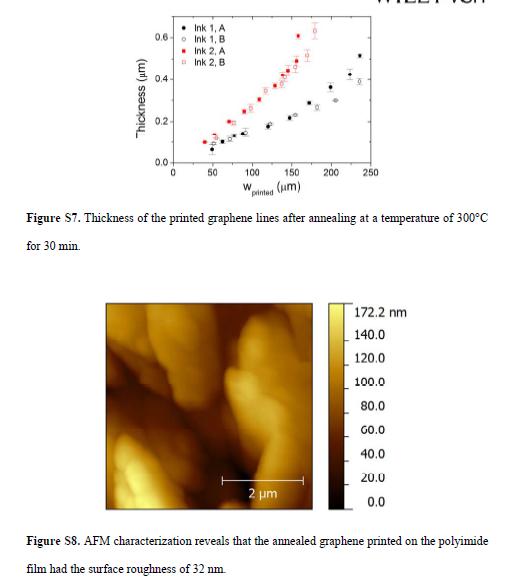
 Thickness of screen-printed graphene lines for different inks and printing directions.")
9 a) OM images of a screen-printed graphene line with w printed of 40 μm and (b e) graphene lines (dark double stripes) with different spacing of 30, 50, 70, and 90 μm on polyimide films. f) Thickness of screen-printed graphene lines for different inks and printing directions. g) Comparison of the aspect ratio (thickness/width) and w printed of the printed graphene lines through a 20 μm wide line opening with respect to the ink viscosity and the printing direction.
10
11 a) OM image of screen-printed graphene to measure electrical properties of the graphene lines for different lengths and w printed. b) Scanning electron microscopy image of the graphene after annealing at a temperature of 300 C for 30 min. c) Resistance per unit length of the graphene as a function of w printed. d) Relative resistance of the screen-printed graphene lines on flexible substrates with two different thicknesses over 1000 bending cycles at a bending radius of 4 mm, corresponding to 1.0% tensile strain.
12
13

14 Application To demonstrate a possible application of screen-printed graphene electrodes, all printed electrolyte-gated transistors (EGTs) were fabricated and characterized. EGTs are promising for flexible printed electronics; the high capacitance of the electrolyte enables low voltage operation, and the material offers broad process compatibility for printing on flexible substrates with high tolerance to thickness variations a) OM image of screen-printed graphene source and drain electrodes on a polyimide substrate for EGTs ( W / L = 900 μm/90 μm). b) Schematic illustration for the EGT architecture fabricated on the graphene electrodes. c) Transfer and d) output characteristics of the printed EGTs. The voltage sweep rate was 50 mv s 1. e) Stability of charge carrier mobility ( μ ) and threshold voltage ( V th ) for the EGTs during repeated bending cycles with a bending radius of 4 mm, corresponding to 1.0% strain.
15 Summary and Conclusion They have demonstrated fine patterning of pristine graphene by screen printing using a silicon stencil and a high conductivity ink based on graphene and EC in terpineol. The well-defined stencil was obtained from a thin silicon wafer by a photolithography process, which was produced with openings as fine as 5 μm on 90-μm-thick silicon wafers. The silicon stencil and ink formulation facilitated screen printing of high quality graphene patterns, achieving a resolution as high as 40 μm, which can be attributed to the fine line opening as well as the tuned viscosity of the graphene ink. The screen-printed graphene lines on polyimide films exhibited high electrical conductivity of S m 1 and outstanding mechanical flexibility, suitable for electronic applications. With the high quality and flexible graphene patterns as source and drain electrodes, allprinted EGTs on flexible substrates showed desirable transfer and output characteristics, as well as durable operation over many bending cycles. Overall, this work establishes a scalable method for the facile and practical printing of highly conductive graphene patterns for flexible and printed electronics.

16
17 A photoresist is a light-sensitive material used in several industrial processes, such as photolithography and photoengraving, to form a patterned coating on a surface Material used: Poly(methyl methacrylate) (PMMA), Poly(methyl glutarimide) (PMGI) Phenol formaldehyde resin, etc,.
NORTHWESTERN UNIVERSITY. Graphene Inks with Cellulosic Dispersants: Development and Applications for Printed Electronics A DISSERTATION
 NORTHWESTERN UNIVERSITY Graphene Inks with Cellulosic Dispersants: Development and Applications for Printed Electronics A DISSERTATION SUBMITTED TO THE GRADUATE SCHOOL IN PARTIAL FULFILLMENT OF THE REQUIREMENTS
Large Scale Direct Synthesis of Graphene on Sapphire and Transfer-free Device Fabrication
 Supplementary Information Large Scale Direct Synthesis of Graphene on Sapphire and Transfer-free Device Fabrication Hyun Jae Song a, Minhyeok Son a, Chibeom Park a, Hyunseob Lim a, Mark P. Levendorf b,
A. Optimizing the growth conditions of large-scale graphene films
 1 A. Optimizing the growth conditions of large-scale graphene films Figure S1. Optical microscope images of graphene films transferred on 300 nm SiO 2 /Si substrates. a, Images of the graphene films grown
Supporting Information for: Sustained sub-60 mv/decade switching via the negative capacitance effect in MoS 2 transistors
 Supporting Information for: Sustained sub-60 mv/decade switching via the negative capacitance effect in MoS 2 transistors Felicia A. McGuire 1, Yuh-Chen Lin 1, Katherine Price 1, G. Bruce Rayner 2, Sourabh
Supporting Information. Fast Synthesis of High-Performance Graphene by Rapid Thermal Chemical Vapor Deposition
 1 Supporting Information Fast Synthesis of High-Performance Graphene by Rapid Thermal Chemical Vapor Deposition Jaechul Ryu, 1,2, Youngsoo Kim, 4, Dongkwan Won, 1 Nayoung Kim, 1 Jin Sung Park, 1 Eun-Kyu
Supporting Information for: Inkjet Printing of High Conductivity, Flexible Graphene Patterns
 Supporting Information for: Inkjet Printing of High Conductivity, Flexible Graphene Patterns Ethan B. Secor, Pradyumna L. Prabhumirashi, Kanan Puntambekar, Michael L. Geier, and,,, * Mark C. Hersam Department
Supporting Information
 Photothermal Effect Induced Negative Photoconductivity and High Responsivity in Flexible Black Phosphorus Transistors Jinshui Miao,, Bo Song,, Qing Li, Le Cai, Suoming Zhang, Weida Hu, Lixin Dong, Chuan
Scaling up Chemical Vapor Deposition Graphene to 300 mm Si substrates
 Scaling up Chemical Vapor Deposition Graphene to 300 mm Si substrates Co- Authors Aixtron Alex Jouvray Simon Buttress Gavin Dodge Ken Teo The work shown here has received partial funding from the European
Inkjet Printed Highly Transparent and Flexible Graphene Micro- Supercapacitors
 Electronic Supplementary Material (ESI) for Nanoscale. This journal is The Royal Society of Chemistry 2017 Inkjet Printed Highly Transparent and Flexible Graphene Micro- Supercapacitors Szymon Sollami
crystals were phase-pure as determined by x-ray diffraction. Atomically thin MoS 2 flakes were
 Nano Letters (214) Supplementary Information for High Mobility WSe 2 p- and n-type Field Effect Transistors Contacted by Highly Doped Graphene for Low-Resistance Contacts Hsun-Jen Chuang, Xuebin Tan, Nirmal
Supplementary Figure 1: Micromechanical cleavage of graphene on oxygen plasma treated Si/SiO2. Supplementary Figure 2: Comparison of hbn yield.
 1 2 3 4 Supplementary Figure 1: Micromechanical cleavage of graphene on oxygen plasma treated Si/SiO 2. Optical microscopy images of three examples of large single layer graphene flakes cleaved on a single
Supplementary information
 Supplementary information Highly Conductive Graphene/Ag Hybrid Fibers for Flexible Fiber-Type Transistors Sang Su Yoon, 1 Kang Eun Lee, 1 Hwa-Jin Cha, 1 Dong Gi Seong, 1 Moon-Kwang Um, 1 Joon Hyung Byun,
Supplementary Figure 1 Dark-field optical images of as prepared PMMA-assisted transferred CVD graphene films on silicon substrates (a) and the one
 and the one") Supplementary Figure 1 Dark-field optical images of as prepared PMMA-assisted transferred CVD graphene films on silicon substrates (a) and the one after PBASE monolayer growth (b). 1 Supplementary Figure
Supplementary Figure 1 Dark-field optical images of as prepared PMMA-assisted transferred CVD graphene films on silicon substrates (a) and the one after PBASE monolayer growth (b). 1 Supplementary Figure
Supplementary Methods A. Sample fabrication
 Supplementary Methods A. Sample fabrication Supplementary Figure 1(a) shows the SEM photograph of a typical sample, with three suspended graphene resonators in an array. The cross-section schematic is
Supporting Information for: Electrical probing and tuning of molecular. physisorption on graphene
 Supporting Information for: Electrical probing and tuning of molecular physisorption on graphene Girish S. Kulkarni, Karthik Reddy #, Wenzhe Zang, Kyunghoon Lee, Xudong Fan *, and Zhaohui Zhong * Department
Supplementary Figure 1 shows overall fabrication process and detailed illustrations are given
 Supplementary Figure 1. Pressure sensor fabrication schematics. Supplementary Figure 1 shows overall fabrication process and detailed illustrations are given in Methods section. (a) Firstly, the sacrificial
Cut-and-Paste Organic FET Customized ICs for Application to Artificial Skin
 Cut-and-Paste Organic FET Customized ICs for Application to Artificial Skin Takao Someya 1, Hiroshi Kawaguchi 2, Takayasu Sakurai 3 1 School of Engineering, University of Tokyo, Tokyo, JAPAN 2 Institute
Supporting Information
 Electronic Supplementary Material (ESI) for ChemComm. This journal is The Royal Society of Chemistry 2014 Supporting Information Controllable Atmospheric Pressure Growth of Mono-layer, Bi-layer and Tri-layer
Electrical Transport Measurements Show Intrinsic Doping and Hysteresis in Graphene p-n Junction Devices
 Electrical Transport Measurements Show Intrinsic Doping and Hysteresis in Graphene p-n Junction Devices Garrett Plunkett Department of Physics Oregon State University June 6, 017 Advisor: Dr. Matthew Graham
Stretchable Graphene Transistors with Printed Dielectrics and Gate Electrodes
 Stretchable Graphene Transistors with Printed Dielectrics and Gate Electrodes Seoung-Ki Lee, Beom Joon Kim, Houk Jang, Sung Cheol Yoon, Changjin Lee, Byung Hee Hong, John A. Rogers, Jeong Ho Cho, Jong-Hyun
Supporting Online Material for
 www.sciencemag.org/cgi/content/full/327/5966/662/dc Supporting Online Material for 00-GHz Transistors from Wafer-Scale Epitaxial Graphene Y.-M. Lin,* C. Dimitrakopoulos, K. A. Jenkins, D. B. Farmer, H.-Y.
Introduction. Photoresist : Type: Structure:
 Photoresist SEM images of the morphologies of meso structures and nanopatterns on (a) a positively nanopatterned silicon mold, and (b) a negatively nanopatterned silicon mold. Introduction Photoresist
Gold Nanoparticles Floating Gate MISFET for Non-Volatile Memory Applications
 Gold Nanoparticles Floating Gate MISFET for Non-Volatile Memory Applications D. Tsoukalas, S. Kolliopoulou, P. Dimitrakis, P. Normand Institute of Microelectronics, NCSR Demokritos, Athens, Greece S. Paul,
Supporting information. Tin dioxide electrolyte-gated transistors working in depletion and enhancement
 Supporting information Tin dioxide electrolyte-gated transistors working in depletion and enhancement mode Irina Valitova 1, Marta Maria Natile 2, Francesca Soavi 3, Clara Santato 4 and Fabio Cicoira 1*
Supporting Information
 Electronic Supplementary Material (ESI) for Journal of Materials Chemistry C. This journal is The Royal Society of Chemistry 2018 Supporting Information Direct Integration of Polycrystalline Graphene on
Supplementary Information. Graphene field-effect transistor array with integrated electrolytic gates. scaled to 200 mm
 Supplementary Information Graphene field-effect transistor array with integrated electrolytic gates scaled to 200 mm N C S Vieira 1,3, J Borme 1, G Machado Jr. 1, F Cerqueira 2, P P Freitas 1, V Zucolotto
Electronic Supplementary Information. Molecular Antenna Tailored Organic Thin-film Transistor for. Sensing Application
 Electronic Supplementary Material (ESI) for Materials Horizons. This journal is The Royal Society of Chemistry 2017 Electronic Supplementary Information Molecular Antenna Tailored Organic Thin-film Transistor
High Performance, Low Operating Voltage n-type Organic Field Effect Transistor Based on Inorganic-Organic Bilayer Dielectric System
 Journal of Physics: Conference Series PAPER OPEN ACCESS High Performance, Low Operating Voltage n-type Organic Field Effect Transistor Based on Inorganic-Organic Bilayer Dielectric System To cite this
Nanocarbon Technology for Development of Innovative Devices
 Nanocarbon Technology for Development of Innovative Devices Shintaro Sato Daiyu Kondo Shinichi Hirose Junichi Yamaguchi Graphene, a one-atom-thick honeycomb lattice made of carbon, and a carbon nanotube,
Supplementary Figures
 Supplementary Figures Supplementary Figure 1 Molecular structures of functional materials involved in our SGOTFT devices. Supplementary Figure 2 Capacitance measurements of a SGOTFT device. (a) Capacitance
Kavli Workshop for Journalists. June 13th, CNF Cleanroom Activities
 Kavli Workshop for Journalists June 13th, 2007 CNF Cleanroom Activities Seeing nm-sized Objects with an SEM Lab experience: Scanning Electron Microscopy Equipment: Zeiss Supra 55VP Scanning electron microscopes
Carbon Nanotube Thin-Films & Nanoparticle Assembly
 Nanodevices using Nanomaterials : Carbon Nanotube Thin-Films & Nanoparticle Assembly Seung-Beck Lee Division of Electronics and Computer Engineering & Department of Nanotechnology, Hanyang University,
Supporting information
 Supporting information Influence of electrolyte composition on liquid-gated carbon-nanotube and graphene transistors By: Iddo Heller, Sohail Chatoor, Jaan Männik, Marcel A. G. Zevenbergen, Cees Dekker,
Supporting Information
 Electronic Supplementary Material (ESI) for ChemComm. This journal is The Royal Society of Chemistry 2014 Supporting Information High-k Polymer/Graphene Oxide Dielectrics for Low-Voltage Flexible Nonvolatile
Molecular Electronics For Fun and Profit(?)
") Molecular Electronics For Fun and Profit(?) Prof. Geoffrey Hutchison Department of Chemistry University of Pittsburgh geoffh@pitt.edu July 22, 2009 http://hutchison.chem.pitt.edu Moore s Law: Transistor
Molecular Electronics For Fun and Profit(?) Prof. Geoffrey Hutchison Department of Chemistry University of Pittsburgh geoffh@pitt.edu July 22, 2009 http://hutchison.chem.pitt.edu Moore s Law: Transistor
Supplementary Materials: Janus Monolayer Transition Metal Dichalcogenides
 Supplementary Materials: Janus Monolayer Transition Metal Dichalcogenides Jing Zhang 1, Shuai Jia 1, Kholmanov Iskandar 2, Liang Dong 3, Dequan Er 3, Weibing Chen 1, Hua Guo 1, Zehua Jin 1, Vivek B. Shenoy
Supporting Information
 Supporting Information Assembly and Densification of Nanowire Arrays via Shrinkage Jaehoon Bang, Jonghyun Choi, Fan Xia, Sun Sang Kwon, Ali Ashraf, Won Il Park, and SungWoo Nam*,, Department of Mechanical
Supplementary information for Nonvolatile Memory Cells Based on MoS 2 /Graphene Heterostructures
 Supplementary information for Nonvolatile Memory Cells Based on MoS 2 /Graphene Heterostructures Simone Bertolazzi, Daria Krasnozhon, Andras Kis * Electrical Engineering Institute, École Polytechnique
Flexible nonvolatile polymer memory array on
 Supporting Information for Flexible nonvolatile polymer memory array on plastic substrate via initiated chemical vapor deposition Byung Chul Jang, #a Hyejeong Seong, #b Sung Kyu Kim, c Jong Yun Kim, a
Enhancing the Performance of Organic Thin-Film Transistor using a Buffer Layer
 Proceedings of the 9th International Conference on Properties and Applications of Dielectric Materials July 19-23, 29, Harbin, China L-7 Enhancing the Performance of Organic Thin-Film Transistor using
Electrochemically Exfoliated Graphene as Solution-Processable, Highly-Conductive Electrodes for Organic Electronics
 Supporting Information Electrochemically Exfoliated Graphene as Solution-Processable, Highly-Conductive Electrodes for Organic Electronics Khaled Parvez, Rongjin Li, Sreenivasa Reddy Puniredd, Yenny Hernandez,
Supplementary Figure S1. AFM images of GraNRs grown with standard growth process. Each of these pictures show GraNRs prepared independently,
 Supplementary Figure S1. AFM images of GraNRs grown with standard growth process. Each of these pictures show GraNRs prepared independently, suggesting that the results is reproducible. Supplementary Figure
Graphene photodetectors with ultra-broadband and high responsivity at room temperature
 SUPPLEMENTARY INFORMATION DOI: 10.1038/NNANO.2014.31 Graphene photodetectors with ultra-broadband and high responsivity at room temperature Chang-Hua Liu 1, You-Chia Chang 2, Ted Norris 1.2* and Zhaohui
Graphene Transistors Fabricated via Transfer-Printing In Device Active-Areas on Large Wafer
 Graphene Transistors Fabricated via Transfer-Printing In Device Active-Areas on Large Wafer NANO LETTERS 2007 Vol. 7, No. 12 3840-3844 Xiaogan Liang, Zengli Fu, and Stephen Y. Chou* NanoStructure Laboratory,
Graphene Oxide Femto Gel Photodetector
 Graphene Oxide Femto Gel Photodetector by Dawood Alsaedi A thesis presented to the University of Waterloo in fulfillment of the thesis requirement for the degree of Master of Applied Science in Electrical
(a) (b) Supplementary Figure 1. (a) (b) (a) Supplementary Figure 2. (a) (b) (c) (d) (e)
 (b) Supplementary Figure 1. (a) (b) (a) Supplementary Figure 2. (a) (b) (c) (d) (e)") (a) (b) Supplementary Figure 1. (a) An AFM image of the device after the formation of the contact electrodes and the top gate dielectric Al 2 O 3. (b) A line scan performed along the white dashed line
(a) (b) Supplementary Figure 1. (a) An AFM image of the device after the formation of the contact electrodes and the top gate dielectric Al 2 O 3. (b) A line scan performed along the white dashed line
Extrinsic Origin of Persistent Photoconductivity in
 Supporting Information Extrinsic Origin of Persistent Photoconductivity in Monolayer MoS2 Field Effect Transistors Yueh-Chun Wu 1, Cheng-Hua Liu 1,2, Shao-Yu Chen 1, Fu-Yu Shih 1,2, Po-Hsun Ho 3, Chun-Wei
Overview of the main nano-lithography techniques
 Overview of the main nano-lithography techniques Soraya Sangiao sangiao@unizar.es Outline Introduction: Nanotechnology. Nano-lithography techniques: Masked lithography techniques: Photolithography. X-ray
Supporting Information
 Fully-Printed Stretchable Thin-Film Transistors and Integrated Logic Circuits Le Cai 1, Suoming Zhang 1, Jinshui Miao 1, Zhibin Yu 2, Chuan Wang 1, * 1 Department of Electrical and Computer Engineering,
SUPPLEMENTARY NOTES Supplementary Note 1: Fabrication of Scanning Thermal Microscopy Probes
 SUPPLEMENTARY NOTES Supplementary Note 1: Fabrication of Scanning Thermal Microscopy Probes Fabrication of the scanning thermal microscopy (SThM) probes is summarized in Supplementary Fig. 1 and proceeds
Wafer Scale Homogeneous Bilayer Graphene Films by. Chemical Vapor Deposition
 Supporting Information for Wafer Scale Homogeneous Bilayer Graphene Films by Chemical Vapor Deposition Seunghyun Lee, Kyunghoon Lee, Zhaohui Zhong Department of Electrical Engineering and Computer Science,
Supplementary Information. Rapid Stencil Mask Fabrication Enabled One-Step. Polymer-Free Graphene Patterning and Direct
 Supplementary Information Rapid Stencil Mask Fabrication Enabled One-Step Polymer-Free Graphene Patterning and Direct Transfer for Flexible Graphene Devices Keong Yong 1,, Ali Ashraf 1,, Pilgyu Kang 1,
TRANSVERSE SPIN TRANSPORT IN GRAPHENE
 International Journal of Modern Physics B Vol. 23, Nos. 12 & 13 (2009) 2641 2646 World Scientific Publishing Company TRANSVERSE SPIN TRANSPORT IN GRAPHENE TARIQ M. G. MOHIUDDIN, A. A. ZHUKOV, D. C. ELIAS,
Wafer-scale fabrication of graphene
 Wafer-scale fabrication of graphene Sten Vollebregt, MSc Delft University of Technology, Delft Institute of Mircosystems and Nanotechnology Delft University of Technology Challenge the future Delft University
Supporting Information
 Supporting Information Monolithically Integrated Flexible Black Phosphorus Complementary Inverter Circuits Yuanda Liu, and Kah-Wee Ang* Department of Electrical and Computer Engineering National University
Intrinsic Electronic Transport Properties of High. Information
 Intrinsic Electronic Transport Properties of High Quality and MoS 2 : Supporting Information Britton W. H. Baugher, Hugh O. H. Churchill, Yafang Yang, and Pablo Jarillo-Herrero Department of Physics, Massachusetts
SUPPLEMENTARY INFORMATION
 In the format provided by the authors and unedited. DOI: 10.1038/NPHOTON.2016.254 Measurement of non-monotonic Casimir forces between silicon nanostructures Supplementary information L. Tang 1, M. Wang
Modulation-Doped Growth of Mosaic Graphene with Single Crystalline. p-n Junctions for Efficient Photocurrent Generation
 Modulation-Doped Growth of Mosaic Graphene with Single Crystalline p-n Junctions for Efficient Photocurrent Generation Kai Yan 1,, Di Wu 1,, Hailin Peng 1, *, Li Jin 2, Qiang Fu 2, Xinhe Bao 2 and Zhongfan
ECE 342 Electronic Circuits. Lecture 6 MOS Transistors
 ECE 342 Electronic Circuits Lecture 6 MOS Transistors Jose E. Schutt-Aine Electrical & Computer Engineering University of Illinois jesa@illinois.edu 1 NMOS Transistor Typically L = 0.1 to 3 m, W = 0.2
Supplementary Figure 1 Experimental setup for crystal growth. Schematic drawing of the experimental setup for C 8 -BTBT crystal growth.
 Supplementary Figure 1 Experimental setup for crystal growth. Schematic drawing of the experimental setup for C 8 -BTBT crystal growth. Supplementary Figure 2 AFM study of the C 8 -BTBT crystal growth
Foundations of MEMS. Chang Liu. McCormick School of Engineering and Applied Science Northwestern University. International Edition Contributions by
 Foundations of MEMS Second Edition Chang Liu McCormick School of Engineering and Applied Science Northwestern University International Edition Contributions by Vaishali B. Mungurwadi B. V. Bhoomaraddi
SUPPLEMENTARY INFORMATION
 Synthesis of monolithic graphene graphite integrated electronics Jang-Ung Park 1,2, SungWoo Nam 3, Mi-Sun Lee 1 & Charles M. Lieber 2,3 1 School of Nano-Biotechnology and Chemical Engineering, School of
Persistent Drought Monitoring Using a Microfluidic-Printed Electro-
 Electronic Supplementary Material (ESI) for Lab on a Chip. This journal is The Royal Society of Chemistry 2017 Supplementary Information Persistent Drought Monitoring Using a Microfluidic-Printed Electro-
Supplementary Information for. Origin of New Broad Raman D and G Peaks in Annealed Graphene
 Supplementary Information for Origin of New Broad Raman D and G Peaks in Annealed Graphene Jinpyo Hong, Min Kyu Park, Eun Jung Lee, DaeEung Lee, Dong Seok Hwang and Sunmin Ryu* Department of Applied Chemistry,
Supplementary Materials for
 advances.sciencemag.org/cgi/content/full/2/9/e1601240/dc1 Supplementary Materials for Quasi-ballistic carbon nanotube array transistors with current density exceeding Si and GaAs Gerald J. Brady, Austin
FLCC Seminar. Spacer Lithography for Reduced Variability in MOSFET Performance
 1 Seminar Spacer Lithography for Reduced Variability in MOSFET Performance Prof. Tsu-Jae King Liu Electrical Engineering & Computer Sciences Dept. University of California at Berkeley Graduate Student:
Especial Bump Bonding Technique for Silicon Pixel Detectors
 Especial Bump Bonding Technique for Silicon Pixel Detectors E. Cabruja, M. Bigas, M. Ullán, G. Pellegrini, M. Lozano Centre Nacional de Microelectrònica Spain Outline Motivation Summary of bump bonding
High-resolution on-chip supercapacitors with ultra-high scan rate ability
 Electronic Supplementary Material (ESI) for Journal of Materials Chemistry A. This journal is The Royal Society of Chemistry 214 Supporting Information High-resolution on-chip supercapacitors with ultra-high
Integrating MEMS Electro-Static Driven Micro-Probe and Laser Doppler Vibrometer for Non-Contact Vibration Mode SPM System Design
 Tamkang Journal of Science and Engineering, Vol. 12, No. 4, pp. 399 407 (2009) 399 Integrating MEMS Electro-Static Driven Micro-Probe and Laser Doppler Vibrometer for Non-Contact Vibration Mode SPM System
Tunneling characteristics of graphene
 Tunneling characteristics of graphene Young Jun Shin, 1,2 Gopinadhan Kalon, 1,2 Jaesung Son, 1 Jae Hyun Kwon, 1,2 Jing Niu, 1 Charanjit S. Bhatia, 1 Gengchiau Liang, 1 and Hyunsoo Yang 1,2,a) 1 Department
Lithography-Free Fabrication of High Quality Substrate- Supported and Freestanding Graphene Devices
 98 DOI 10.1007/s12274-010-1013-5 Research Article Lithography-Free Fabrication of High Quality Substrate- Supported and Freestanding Graphene Devices Wenzhong Bao 1, Gang Liu 1, Zeng Zhao 1, Hang Zhang
Supporting Information
 Supporting Information Flexible, Cuttable and Self-Waterproof Bending Strain Sensors Using Microcracked Gold Nanofilms@Paper Substrate Xinqin Liao, 1, Zheng Zhang, 1, Qijie Liang, 1 Qingliang Liao, 1,
Transport of Electrons on Liquid Helium across a Tunable Potential Barrier in a Point Contact-like Geometry
 Journal of Low Temperature Physics - QFS2009 manuscript No. (will be inserted by the editor) Transport of Electrons on Liquid Helium across a Tunable Potential Barrier in a Point Contact-like Geometry
Black phosphorus: A new bandgap tuning knob
 Black phosphorus: A new bandgap tuning knob Rafael Roldán and Andres Castellanos-Gomez Modern electronics rely on devices whose functionality can be adjusted by the end-user with an external knob. A new
Supporting information. Gate-optimized thermoelectric power factor in ultrathin WSe2 single crystals
 Supporting information Gate-optimized thermoelectric power factor in ultrathin WSe2 single crystals Masaro Yoshida 1, Takahiko Iizuka 1, Yu Saito 1, Masaru Onga 1, Ryuji Suzuki 1, Yijin Zhang 1, Yoshihiro
Authors: D.S.Roveri 1, H.H.Bertan 1, M.A.R.Alves 1, J.F.Mologni 2, E.S.Braga 1
 Use of Ansoft Maxwell software platform for investigation of electrostatic properties of a hemisphere on a post geometry aimed to model field emission devices Authors: D.S.Roveri 1, H.H.Bertan 1, M.A.R.Alves
Low Power Phase Change Memory via Block Copolymer Self-assembly Technology
 Low Power Phase Change Memory via Block Copolymer Self-assembly Technology Beom Ho Mun 1, Woon Ik Park 1, You Yin 2, Byoung Kuk You 1, Jae Jin Yun 1, Kung Ho Kim 1, Yeon Sik Jung 1*, and Keon Jae Lee 1*
Technology Brief 9: Capacitive Sensors
 218 TEHNOLOGY BRIEF 9: APAITIVE SENSORS Technology Brief 9: apacitive Sensors To sense is to respond to a stimulus. (See Tech Brief 7 on resistive sensors.) A capacitor can function as a sensor if the
30-Inch Roll-Based Production of High-Quality Graphene Films for Flexible Transparent Electrodes
 30-Inch Roll-Based Production of High-Quality Graphene Films for Flexible Transparent Electrodes Sukang Bae, 1* Hyeong Keun Kim, 3* Xianfang Xu, 5 Jayakumar Balakrishnan, 5 Tian Lei, 1 Young Il Song, 6
2D Materials for Gas Sensing
 2D Materials for Gas Sensing S. Guo, A. Rani, and M.E. Zaghloul Department of Electrical and Computer Engineering The George Washington University, Washington DC 20052 Outline Background Structures of
High Energy Density of All Screen-Printable Solid-State. Microsupercapacitor Integrated by Graphene/CNTs as. Hierarchical Electrodes
 Electronic Supplementary Material (ESI) for Journal of Materials Chemistry A. This journal is The Royal Society of Chemistry 2019 Supporting information High Energy Density of All Screen-Printable Solid-State
100 nm period gratings produced by lithographically induced self-construction
 INSTITUTE OFPHYSICS PUBLISHING Nanotechnology 14 (2003) 786 790 NANOTECHNOLOGY PII: S0957-4484(03)55891-3 100 nm period gratings produced by lithographically induced self-construction Xinya Lei, Lin Wu,
Beyond silicon electronics-fets with nanostructured graphene channels with high on-off ratio and highmobility
 Beyond silicon electronics-fets with nanostructured graphene channels with high on-off ratio and highmobility M.Dragoman 1, A.Dinescu 1, and D.Dragoman 2 1 National Institute for Research and Development
MoS 2 Thin Film Transistors using PECVD Dielectrics and Optical Contrast Modeling for Thickness Measurement
 MoS 2 Thin Film Transistors using PECVD Dielectrics and Optical Contrast Modeling for Thickness Measurement by Nicholas Vardy A thesis presented to the University of Waterloo in fulfillment of the thesis
Institute for Electron Microscopy and Nanoanalysis Graz Centre for Electron Microscopy
 Institute for Electron Microscopy and Nanoanalysis Graz Centre for Electron Microscopy Micromechanics Ass.Prof. Priv.-Doz. DI Dr. Harald Plank a,b a Institute of Electron Microscopy and Nanoanalysis, Graz
Lecture 150 Basic IC Processes (10/10/01) Page ECE Analog Integrated Circuits and Systems P.E. Allen
 Page ECE Analog Integrated Circuits and Systems P.E. Allen") Lecture 150 Basic IC Processes (10/10/01) Page 1501 LECTURE 150 BASIC IC PROCESSES (READING: TextSec. 2.2) INTRODUCTION Objective The objective of this presentation is: 1.) Introduce the fabrication of
Lecture 150 Basic IC Processes (10/10/01) Page 1501 LECTURE 150 BASIC IC PROCESSES (READING: TextSec. 2.2) INTRODUCTION Objective The objective of this presentation is: 1.) Introduce the fabrication of
2D-2D tunneling field effect transistors using
 2D-2D tunneling field effect transistors using WSe 2 /SnSe 2 heterostructures Tania Roy, 1,2,3 Mahmut Tosun, 1,2,3 Mark Hettick, 1,2,3, Geun Ho Ahn, 1,2,3 Chenming Hu 1, and Ali Javey 1,2,3, 1 Electrical
Supporting Information. Direct n- to p-type Channel Conversion in Monolayer/Few-Layer WS 2 Field-Effect Transistors by Atomic Nitrogen Treatment
 Supporting Information Direct n- to p-type Channel Conversion in Monolayer/Few-Layer WS 2 Field-Effect Transistors by Atomic Nitrogen Treatment Baoshan Tang 1,2,, Zhi Gen Yu 3,, Li Huang 4, Jianwei Chai
Initial Stages of Growth of Organic Semiconductors on Graphene
 Initial Stages of Growth of Organic Semiconductors on Graphene Presented by: Manisha Chhikara Supervisor: Prof. Dr. Gvido Bratina University of Nova Gorica Outline Introduction to Graphene Fabrication
Ion Implantation. alternative to diffusion for the introduction of dopants essentially a physical process, rather than chemical advantages:
 Ion Implantation alternative to diffusion for the introduction of dopants essentially a physical process, rather than chemical advantages: mass separation allows wide varies of dopants dose control: diffusion
Arrays of Size-Selected Metal Nanoparticles Formed by Cluster Ion Beam Technique
 MRS Advances 2018 Materials Research Society DOI: 10.1557/adv.2018.427 Arrays of Size-Selected Metal Nanoparticles Formed by Cluster Ion Beam Technique Florian A. Ceynowa 1,2, Manohar Chirumamilla 1, Vladimir
Patterned PtNWs Film. CE WE: PtNWs. Red. SiO 2 /Si
 . Supplementary Figures Device Fabrication. Film Deposition 2. Template Removal. PMMA Deposition 2. Window Opening Patterned Au Electrodes with PMMA Window Patterned PtNWs Film PtNWs Device with PMMA Window
Supplementary Materials for
 advances.sciencemag.org/cgi/content/full/3/9/e1701222/dc1 Supplementary Materials for Moisture-triggered physically transient electronics Yang Gao, Ying Zhang, Xu Wang, Kyoseung Sim, Jingshen Liu, Ji Chen,
Synthesis of Monolithic Graphene Graphite Integrated Electronics
 Synthesis of Monolithic Graphene Graphite Integrated Electronics The Harvard community has made this article openly available. Please share how this access benefits you. Your story matters Citation Park,
A Low-Noise Solid-State Nanopore Platform Based on a Highly Insulating Substrate
 SUPPORTING INFORMATION A Low-Noise Solid-State Nanopore Platform Based on a Highly Insulating Substrate Min-Hyun Lee, Ashvani Kumar, Kyeong-Beom Park, Seong-Yong Cho, Hyun-Mi Kim, Min-Cheol Lim, Young-Rok
Supplementary information for Tunneling Spectroscopy of Graphene-Boron Nitride Heterostructures
 Supplementary information for Tunneling Spectroscopy of Graphene-Boron Nitride Heterostructures F. Amet, 1 J. R. Williams, 2 A. G. F. Garcia, 2 M. Yankowitz, 2 K.Watanabe, 3 T.Taniguchi, 3 and D. Goldhaber-Gordon
Supporting Information. Metallic Adhesion Layer Induced Plasmon Damping and Molecular Linker as a Non-Damping Alternative
 Supporting Information Metallic Adhesion Layer Induced Plasmon Damping and Molecular Linker as a Non-Damping Alternative Terefe G. Habteyes, Scott Dhuey, Erin Wood, Daniel Gargas, Stefano Cabrini, P. James
Photolithography Overview 9/29/03 Brainerd/photoclass/ECE580/Overvie w/overview
 http://www.intel.com/research/silicon/mooreslaw.htm 1 Moore s law only holds due to photolithography advancements in reducing linewidths 2 All processing to create electric components and circuits rely
Large scale growth and characterization of atomic hexagonal boron. nitride layers
 Supporting on-line material Large scale growth and characterization of atomic hexagonal boron nitride layers Li Song, Lijie Ci, Hao Lu, Pavel B. Sorokin, Chuanhong Jin, Jie Ni, Alexander G. Kvashnin, Dmitry
Supporting Information
 Electronic Supplementary Material (ESI) for Nanoscale. This journal is The Royal Society of Chemistry 215 Supporting Information Enhanced Photovoltaic Performances of Graphene/Si Solar Cells by Insertion