The Sensitivity Limits of Nanowire Biosensors
|
|
|
- Olivia Cross
- 5 years ago
- Views:
Transcription
1 The Sensitivity Limits of Nanowire Biosensors Xuan Gao Dept of Chemistry and Chemical Biology, Harvard University Jan. 15 th, 2007 Texas A&M University


2 Why Nano for Bio-detection? Protein/DNA Virus Cell 0.1 1nm μm 10 Nanoarrays/assembles Nanodots, wires Nano high sensitivity! Sensitivity matters: early diagnostics of disease (low concentration protein detection); genomics (e.g. DNA sequencing); biophysics research (e.g. single molecule techniques)
3 utline 1. Motivation and introduction 2. Nanowire FET biosensors: sensitivity limits? A fundamental analysis: importance of length scales Pushing sensitivity limits: ph, protein detections Charge detection limits 3. Noise spectroscopy for bio-reaction 4. Perspective/Future directions


 Dai group, PNAS")
4 Nano for bio-detection: what have been demonstrated Bio-bar-coded nanoparticle Micromechanical device Surf plasmon reson. of nanoparticle Mirkin group, Science 2003 Fritz et al., Science 2000 Chilkoti, Anal Chem 2004 Carbon Nanotube FET Nanowire FET Main idea: Low concentration molecule binding on surface Large change in physical properties of volume (high surface-volume ratio) Dai group, PNAS 2003 Lieber group, Science 2003; Nat. Biotech 2005
 Doped p-type")
 600 400 200 0-200 -400-600 -1.0-0.5 0.0 0.5 1.")
 e.g. L.J. Lauhon et al., Nature 420, 57 (2002). e.g. S.Jin et al.")
5 Nanowire synthesis and FET fabrication CVD synthesis of Si-nanowire Nanowire Field-Effect-Transistor SiH 4 Au Si 3 N 4 Passivation layer (~60 nm) Doped p-type Si Nanowire 60 nm Ni for source and drain S D Substrate or back gate Channel length ~ 2 μm 5 nm I sd (na) V sd (V) V sd (V) G (ns) V g (V) Back gate V g (V) e.g. L.J. Lauhon et al., Nature 420, 57 (2002). e.g. S.Jin et al., Nano Lett. 4, 915 (2004).


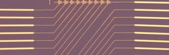
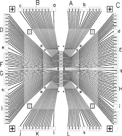
6 NW-FET sensor array chip Si-NW S D 100um G buffer sample time
7 Nanowire FET as biosensor: basic principle analyte s nanowire substrate d - s nanowire substrate d I sd or G I sd or G The field effect of molecule binding acts as a gate voltage time time
8 Nanowire FET as biosensor: sensitivity limits? analyte s nanowire substrate d - s nanowire substrate d I sd or G I sd or G The field effect of molecule binding acts as a gate voltage time time NanowireFET sensor: ultrasensitive, label-free, real-time, and multiplexible What is the fundamental limit of sensitivity/response? (That s why nano matters!)
 40 20 10 8 6 4 2 0.8 1 0.6 Volume conductance G p πr 2 Debye screening length: Debye ΔG/G λ/r (surface-volume ratio effect!")
9 NW-FET sensitivity: the role of carrier screening R E c ~λ E i E F E v High carrier density, λ<r NW carrier density&conductance changes in depth ~λ near surface. ΔG ~ Δp 2πR λ s d screening length λ (nm) Volume conductance G p πr 2 Debye screening length: Debye ΔG/G λ/r (surface-volume ratio effect!) λ= εk B T pe 2 Screening length λ for p-silicon Typical R of NW Thomas-Fermi p (cm -3 ) Typical doping level
")
10 NW-FET sensitivity: the role of carrier screening Δϕ R E F Low carrier density, λ>r Analyte molecules at surface gate the whole volume of nanowire s d screening length λ (nm) Debye screening length: Debye λ= εk B T pe 2 Screening length λ for p-silicon Typical R of NW Thomas-Fermi p (cm -3 )
11 Nanowire-FET sensors: the limiting response R s d Δϕ E F 1. Non-degenerate semiconductors: p = p i {exp(e i -E F )/k B T } 2. NW conductance G = p πr 2 eμ /L Low carrier density, λ>r Analyte molecules at surface gate the whole volume of nanowire NW sensor has the limiting (most sensitive) response in the long screening length regime: ΔG/G = exp(δϕ/kt)-1
12 NW-FET sensitivity: the role of carrier screening R R E c E i Reduce R, increase λ Δϕ ~λ E F E v Δϕ E F λ<r Molecules on surface gate ~λ depth into nanowire λ>r Molecules on surface gate the whole volume of nanowire ΔG/G exp(δϕ/kt)-1
 solution gate V g (V) 1000 100 10 Subthreshold 1 screening length λ (nm) 60 40 20 10 8 6 4 2 0.")
13 λ>r is reached in the subthreshold regime Gate voltage V g G (ns) V g s Linear regime g H 2 d Threshold voltage water gate V g (V) solution gate V g (V) Subthreshold 1 screening length λ (nm) Subthreshold regime λ>r R λ<r Linear regime p (cm -3 ) NW sensor has the limiting (most sensitive) response in the long screening length (λ>r) regime: ΔG/G = exp(δϕ/kt)-1
14 Nanowire sensor: ph Sensing ~ V sd Δϕ solution ph = -log 10 [H ] Gate/reference electrode - Double layer Si-H Si- - H NH 2 H NH 3
15 Pushing Sensitivity of Nanowire Sensors: ph sensing nm diameter p-type silicon NW ΔG/G (%) time (s) ph 9 40% G (ns) Vg (V)
16 Pushing Sensitivity of Nanowire Sensors: ph sensing nm diameter p-type silicon NW ΔG/G (%) time (s) ph 9 150% 40% G (ns) Vg (V)
17 Pushing Sensitivity of Nanowire Sensors: ph sensing 10nm diameter p-type silicon NW ΔG/G (%) subthreshold near threshold linear regime time (s) 7 ph 9 600% 150% 40% G (ns) Vg (V)
18 Pushing Sensitivity of Nanowire Sensors: ph sensing ΔG/G = exp(δϕ /kt)-1 for Δϕ =30mV/pH 1000 Δϕ 1000 Linear subthreshold G (ns) Δϕ Vg (V) 0.1 ΔG= Δϕ g m for Δϕ=30mV/pH Every ph change is equivalent to 30mV Vg shift in both regimes (also true for different NW diameter, doping level, etc.)
19 Pushing Sensitivity of Nanowire Sensors: ph sensing ΔG/G = exp(δϕ /kt)-1 for Δϕ =30mV/pH Electrochemical potential: μ ec = qϕ k B T ln ([H ] s /[H ] b ) Linear subthreshold Δϕ =k B T/q ln(10) ΔpH bulk ~59mV/pH If ph surface can be kept constant ph surface ΔG/G= Δϕ g m /G for Δϕ=30mV/pH ph bulk Si-H Si- - H NH 2 H NH 3 Δϕ
20 Pushing Sensitivity of Nanowire Sensors: ph sensing summary ΔG/G (%) subthreshold near threshold linear regime time (s) 7 ph 9 For chemical reaction induced Δϕ: The strongest response is indeed observed in subthreshold regime and ΔG/G = exp (Δϕ /kt)-1 chemistry doesn t change (Δϕ=const.)! E c E F E F ~λ E v Linear regime Subthreshold regime
21 Cancer marker protein sensing -surface modification HH H H H H Et Et Si C Et H (1% in 95% EtH) C Si H C Si H (1) Silane modification (2) Antibody modification NH 2 CNBH 3 in binding buffer (10mM, ph 8.4) F. Patolsky et al, Nat. Protocols 1, 1711 (2006). (3) Silane blocking H NH 2 CNBH 3 in binding buffer (10mM, ph 8.4) H H H NH C H H NH C H H NH C H H NH C H Si Si (4) Sensing Si Si in assay buffer (10uM, ph 7.1)
22 Cancer marker protein sensing - antibody - antigen G (μs) ΔG PSA 150 nm 15 nm 1.5 nm 150 pm 15 pm 1.5 pm buffer 1.30 k a [Ab] [PSA] [Ab/PSA] k d Time (s) [Ab/PSA] eq = [Ab]*[PSA] K d [PSA] Disassociation constant K d =k d /k a K d ~ nms (e.g. Saerens et al, J. Bio. Chem. 2004) ΔG (ns) n 100n 150n K d 1p 10p 100p 1n 10n 100n PSA concentration (M)
23 Pushing Sensitivity of Nanowire Sensors -cancer marker protein sensing - antibody - antigen 15 pm PSA buffer buffer G (ns) nS/V in linear regime mV/dec 10 Linear regime Vg (V) For a given protein concentration, detection is greatly improved in the subthreshold regime! Subthreshold regime (Δϕ~15mV for 15pM PSA in both regimes)
24 Pushing Sensitivity of Nanowire Sensors -cancer marker protein sensing ΔG/G (%) antibody - antigen 15pM PSA threshold voltage e Δϕ /kt -1 G (ns) nS/V in linear regime Vg (V) 110mV/dec signal noise ratio For a given protein concentration, detection is greatly improved in the subthreshold regime! V g (V) (Δϕ~15mV for 15pM PSA in both regimes)
 Time (s) Detection limit reduced from")
25 Nanowire Sensor detection limits -linear vs. subthreshold regime PSA detection in linear regime PSA detection in subthreshold regime PSA Time (s) Time (s) Detection limit reduced from pms to fms by operating nanowire sensor in the subthreshold regime where screening length λ>r!
26 Charge Sensitivity of Nanowire Sensors ΔQ Δϕ Surface charge detected: ΔQ= [C DL 1/(C -1 Si2 C -1 NW )] Δϕ L C DL Δϕ C NW C Si2
27 Charge Sensitivity of Nanowire Sensors ΔQ Δϕ 100 μm buffer R=λ Si R=5λ Si Surface charge detected: ΔQ= [C DL 1/(C -1 Si2 C -1 NW )] Δϕ L Solving Poisson-Boltzmann equation Δp(r), Δϕ(r) nm C DL Δϕ C NW C Si2
28 Charge Sensitivity of Nanowire Sensors ΔQ Δϕ 100 μm buffer R=λ Si R=5λ Si Surface charge detected: ΔQ= [C DL 1/(C -1 Si2 C -1 NW )] Δϕ L Solving Poisson-Boltzmann equation Δp(r), Δϕ(r) nm Q C NW NW R = Δ p e 2πrdr 0 = dq NW / dδϕ C DL Δϕ C Si2 λ DL C NW For R~10nm, L=1μm C NW : ff afs C DL : ffs C Si2 : ~ffs C NW e 2 (pπr 2 )/k B T 2λ Si /R, high p C NW e 2 (pπr 2 )/k B T, low p hole density per unit length of NW
29 Charge Sensitivity of Nanowire Sensors ΔQ Δϕ 100 μm buffer R=λ Si R=5λ Si Surface charge detected: ΔQ= [C DL 1/(C -1 Si2 C -1 NW )] Δϕ L C DL Δϕ L (in subthreshold) 2πε/ln(1λ DL /R) Δϕ L ε=80, L: device length, R: nanowire radius nm Δϕ min Linear Subthreshold 5mV 0.66mV C DL Δϕ C Si2 λ DL C NW For R~10nm, L=1μm C NW : ff afs C DL : ffs C Si2 : ~ffs ΔQ min (I.S.=10mM) ΔQ min (I.S.=10μM) ~300e ~40e ~50e ~6e * Calculated for per μm NW with R=10nm
30 utline 1. Motivation and introduction 2. Nanowire FET biosensors: sensitivity limits? A fundamental analysis: importance of length scales Pushing sensitivity limits: ph, protein detections Charge detection limits 3. Noise spectroscopy for bio-reaction 4. Perspective/Future directions
31 Nanowire FET noise as a probe for biochemical reactions--motivation Fluctuation dissipation theorem: the response of a system to an external perturbation is related to the fluctuations of the system in thermal equilibrium. cantilever stage R Noise power (A 2 ) ω reson ~Q -1 Johnson noise R or T AFM tip noise ω reson & Q Hutter, Bechhoefer RSI (1993). spin noise hyperfine splittings Crooker et al, Nature (2004). Noise can give useful information without disturbing the system!


32 Nanowire FET noise as a probe for biochemical reactions--motivation Fluctuation dissipation theorem: the response of a system to an external perturbation is related to the fluctuations of the system in thermal equilibrium. Can we obtain reaction kinetics from the noise of bio-sensors at equilibrium? binding unbinding Buffer Sample Buffer? Reaction Kinetics k a [Ab] [Ag] [Ab/Ag] k d
33 Protein binding induced Lorentzian noise G ( μs) pm 150 pm real-time 5 pm 0.15 pm S /f buffer 1/f S G 5nM = Time (s) 10 12x f (Hz) f (Hz) S pM G = 3700 S G 5pM = 4000 S pm G = pM PSA f (Hz) f (Hz) τ e t Time domain 2 2 τ f ; τ ~1 ms f (Hz) PSA binding/unbinding at equilibrium adds a Lorentzian noise to the 1/f noise of NW. Lorentzian noise still presents in low concentrations which are not detectable in time domain
34 Summary 1. Sensitivity limits of nanowire biosensors Where to achieve the best sensitivity?-subthreshold. reduced carrier screening efficient molecule gating; ΔG/G exp(δϕ /kt)-1. Pushing sensitivity limits: ph, protein detections pm PSA (linear) fm PSA detection (subthreshold) Charge detection limits (a few e s) 2. Probing bio-reaction by device noise protein binding induced Lorentzian noise S ~λ E c E F E v vs. 15 pm PSA subthreshold Linear regime 1/f E F Linear f (Hz) buffer 1/f 0.15 pm G = 3600 PSA S Subthreshold f (Hz)
35 Nanowire Research: Future Directions (1) Towards single molecule detection and reaction dynamics study G Bio-Apps single molecule study reaction dynamics capacitance sensing biomolecule manipulation and electrokinetics protein/dna/cell Initial approaches: higher mobility / shorter channel devices; suthreshold regime sensing G τ on time τ off Label free & direct electrical study of single biomolecules and their reaction dynamics
36 Nanowire Research: Future Directions (2) capacitance sensing (ε effect); Bio-Apps single molecule study reaction dynamics capacitance sensing biomolecule manipulation and electrokinetics protein/dna/cell capacitance bridge Conductance charge of biomolecules Capacitance dielectric properties of biomolecules
 Hetero-structures will enable novel physics study in clean ( ballistic ) 1D nanostructures How to directly probe")
37 Nanowire Research: Future Directions Physics G(μS) Quantized at low T! diffusive vs. ballistic transport in 1D single particle vs. many-body thermal/thermoelectric properties charge vs. spin transport 1D hole gas, Lu et al, PNAS 2005, Xiang et al, Nature 2006 V g (V) Hetero-structures will enable novel physics study in clean ( ballistic ) 1D nanostructures How to directly probe ballistic holes in NW? How about heat transport?...

38 Nanowire Research: Future Directions Development new materials, structures addressable arrays micro-fluidics, lab on a chip novel devices, energy solutions Bio-Apps proteomics, genomics drug discovery, cell biology single molecule study reaction dynamics capacitance sensing biomolecule manipulation Physics and electrokinetics protein/dna/cell G τ on τ off time diffusive vs. ballistic single particle vs. many-body charge vs. spin transport electric/thermal properties C

39 Acknowledgement Dr. GengFeng Zheng Prof. Charles Lieber The Lieber group Thank You!
Nanoscale electrochemistry
 Electrical characterisation of nanoscale samples & biochemical interfaces: methods and electronic instrumentation Nanoscale electrochemistry Giorgio Ferrari Dipartimento di elettronica, informazione e
There's Plenty of Room at the Bottom
 There's Plenty of Room at the Bottom 12/29/1959 Feynman asked why not put the entire Encyclopedia Britannica (24 volumes) on a pin head (requires atomic scale recording). He proposed to use electron microscope
Electrostatics of Nanowire Transistors
 Electrostatics of Nanowire Transistors Jing Guo, Jing Wang, Eric Polizzi, Supriyo Datta and Mark Lundstrom School of Electrical and Computer Engineering Purdue University, West Lafayette, IN, 47907 ABSTRACTS
Supplementary Figure S1. AFM images of GraNRs grown with standard growth process. Each of these pictures show GraNRs prepared independently,
 Supplementary Figure S1. AFM images of GraNRs grown with standard growth process. Each of these pictures show GraNRs prepared independently, suggesting that the results is reproducible. Supplementary Figure
/ / Fields, Forces and Flows in Biological Systems
 20.330 / 6.023 / 2.793 Fields, Forces and Flows in Biological Systems Instructors: Jongyoon Jay Han and Scott Manalis TOPICS Introduction to electric fields Maxwell s equations Introduction to fluid flows
Semiconductor Physics Problems 2015
 Semiconductor Physics Problems 2015 Page and figure numbers refer to Semiconductor Devices Physics and Technology, 3rd edition, by SM Sze and M-K Lee 1. The purest semiconductor crystals it is possible
Carbon Nanotube Based Aqueous Ion and ph Sensor
 Carbon Nanotube Based Aqueous Ion and ph Sensor Suchit Bhattarai, Konrad H. Aschenbach, Dr. Romel D. Gomez Abstract This study characterizes the response of carbon nanotube (CNT) based biosensor FET chips
ESE 570: Digital Integrated Circuits and VLSI Fundamentals
 ESE 570: Digital Integrated Circuits and VLSI Fundamentals Lec 4: January 23, 2018 MOS Transistor Theory, MOS Model Penn ESE 570 Spring 2018 Khanna Lecture Outline! CMOS Process Enhancements! Semiconductor
MOS Capacitor MOSFET Devices. MOSFET s. INEL Solid State Electronics. Manuel Toledo Quiñones. ECE Dept. UPRM.
 INEL 6055 - Solid State Electronics ECE Dept. UPRM 20th March 2006 Definitions MOS Capacitor Isolated Metal, SiO 2, Si Threshold Voltage qφ m metal d vacuum level SiO qχ 2 E g /2 qφ F E C E i E F E v qφ
Fundamentals of the Metal Oxide Semiconductor Field-Effect Transistor
 Triode Working FET Fundamentals of the Metal Oxide Semiconductor Field-Effect Transistor The characteristics of energy bands as a function of applied voltage. Surface inversion. The expression for the
Electric Field-Dependent Charge-Carrier Velocity in Semiconducting Carbon. Nanotubes. Yung-Fu Chen and M. S. Fuhrer
 Electric Field-Dependent Charge-Carrier Velocity in Semiconducting Carbon Nanotubes Yung-Fu Chen and M. S. Fuhrer Department of Physics and Center for Superconductivity Research, University of Maryland,
ECE 340 Lecture 39 : MOS Capacitor II
 ECE 340 Lecture 39 : MOS Capacitor II Class Outline: Effects of Real Surfaces Threshold Voltage MOS Capacitance-Voltage Analysis Things you should know when you leave Key Questions What are the effects
Controlled Synthesis of Millimeter-Long Silicon Nanowires with Uniform Electronic Properties
 Controlled Synthesis of Millimeter-Long Silicon Nanowires with Uniform Electronic Properties NANO LETTERS 2008 Vol. 8, No. 9 3004-3009 Won Il Park,*, Gengfeng Zheng, Xiaocheng Jiang, Bozhi Tian, and Charles
Quantifying the Affinities and Kinetics of Protein Interactions Using Silicon Nanowire Biosensors
 SUPPLEMENTARY INFORMATION DOI: 10.1038/NNANO.2012.82 Quantifying the Affinities and Kinetics of Protein Interactions Using Silicon Nanowire Biosensors Xuexin Duan, Yue Li, Nitin K. Rajan, David A. Routenberg,
A final review session will be offered on Thursday, May 10 from 10AM to 12noon in 521 Cory (the Hogan Room).
.") A final review session will be offered on Thursday, May 10 from 10AM to 12noon in 521 Cory (the Hogan Room). The Final Exam will take place from 12:30PM to 3:30PM on Saturday May 12 in 60 Evans.» All of
A final review session will be offered on Thursday, May 10 from 10AM to 12noon in 521 Cory (the Hogan Room). The Final Exam will take place from 12:30PM to 3:30PM on Saturday May 12 in 60 Evans.» All of
Metallic: 2n 1. +n 2. =3q Armchair structure always metallic = 2
 Properties of CNT d = 2.46 n 2 2 1 + n1n2 + n2 2π Metallic: 2n 1 +n 2 =3q Armchair structure always metallic a) Graphite Valence(π) and Conduction(π*) states touch at six points(fermi points) Carbon Nanotube:
Electrical Characteristics of MOS Devices
 Electrical Characteristics of MOS Devices The MOS Capacitor Voltage components Accumulation, Depletion, Inversion Modes Effect of channel bias and substrate bias Effect of gate oide charges Threshold-voltage
Nanopores and Nanofluidics for Single DNA Studies Derek Stein Department of Physics Brown University
 Nanopores and Nanofluidics for Single DNA Studies Derek Stein Department of Physics Brown University Overview Motivation: biological, physical, and technological The program: develop and characterize new
ESE 570: Digital Integrated Circuits and VLSI Fundamentals
 ESE 570: Digital Integrated Circuits and VLSI Fundamentals Lec 4: January 29, 2019 MOS Transistor Theory, MOS Model Penn ESE 570 Spring 2019 Khanna Lecture Outline! CMOS Process Enhancements! Semiconductor
Chapter 5 Nanomanipulation. Chapter 5 Nanomanipulation. 5.1: With a nanotube. Cutting a nanotube. Moving a nanotube
 Objective: learn about nano-manipulation techniques with a STM or an AFM. 5.1: With a nanotube Moving a nanotube Cutting a nanotube Images at large distance At small distance : push the NT Voltage pulse
(a) (b) Supplementary Figure 1. (a) (b) (a) Supplementary Figure 2. (a) (b) (c) (d) (e)
 (b) Supplementary Figure 1. (a) (b) (a) Supplementary Figure 2. (a) (b) (c) (d) (e)") (a) (b) Supplementary Figure 1. (a) An AFM image of the device after the formation of the contact electrodes and the top gate dielectric Al 2 O 3. (b) A line scan performed along the white dashed line
(a) (b) Supplementary Figure 1. (a) An AFM image of the device after the formation of the contact electrodes and the top gate dielectric Al 2 O 3. (b) A line scan performed along the white dashed line
Final Examination EE 130 December 16, 1997 Time allotted: 180 minutes
 Final Examination EE 130 December 16, 1997 Time allotted: 180 minutes Problem 1: Semiconductor Fundamentals [30 points] A uniformly doped silicon sample of length 100µm and cross-sectional area 100µm 2
Electronic transport in low dimensional systems
 Electronic transport in low dimensional systems For example: 2D system l
Developing Quantum Logic Gates: Spin-Resonance-Transistors
 Developing Quantum Logic Gates: Spin-Resonance-Transistors H. W. Jiang (UCLA) SRT: a Field Effect Transistor in which the channel resistance monitors electron spin resonance, and the resonance frequency
! CMOS Process Enhancements. ! Semiconductor Physics. " Band gaps. " Field Effects. ! MOS Physics. " Cut-off. " Depletion.
 ESE 570: Digital Integrated Circuits and VLSI Fundamentals Lec 4: January 3, 018 MOS Transistor Theory, MOS Model Lecture Outline! CMOS Process Enhancements! Semiconductor Physics " Band gaps " Field Effects!
How a single defect can affect silicon nano-devices. Ted Thorbeck
 How a single defect can affect silicon nano-devices Ted Thorbeck tedt@nist.gov The Big Idea As MOS-FETs continue to shrink, single atomic scale defects are beginning to affect device performance Gate Source
single-electron electron tunneling (SET)
") single-electron electron tunneling (SET) classical dots (SET islands): level spacing is NOT important; only the charging energy (=classical effect, many electrons on the island) quantum dots: : level spacing
single-electron electron tunneling (SET) classical dots (SET islands): level spacing is NOT important; only the charging energy (=classical effect, many electrons on the island) quantum dots: : level spacing
Lecture 4. Conductance sensors. ChemFET. Electrochemical Impedance Spectroscopy. py Practical consideration for electrochemical biosensors.
 Lecture 4 Conductance sensors. ChemFET. Electrochemical Impedance Spectroscopy. py Practical consideration for electrochemical biosensors. Conductivity I V = I R=, L - conductance L= κa/, l Λ= κ /[ C]
EECS130 Integrated Circuit Devices
 EECS130 Integrated Circuit Devices Professor Ali Javey 10/30/2007 MOSFETs Lecture 4 Reading: Chapter 17, 19 Announcements The next HW set is due on Thursday. Midterm 2 is next week!!!! Threshold and Subthreshold
NiCl2 Solution concentration. Etching Duration. Aspect ratio. Experiment Atmosphere Temperature. Length(µm) Width (nm) Ar:H2=9:1, 150Pa
 Width (nm) Ar:H2=9:1, 150Pa") Experiment Atmosphere Temperature #1 # 2 # 3 # 4 # 5 # 6 # 7 # 8 # 9 # 10 Ar:H2=9:1, 150Pa Ar:H2=9:1, 150Pa Ar:H2=9:1, 150Pa Ar:H2=9:1, 150Pa Ar:H2=9:1, 150Pa Ar:H2=9:1, 150Pa Ar:H2=9:1, 150Pa Ar:H2=9:1,
Experiment Atmosphere Temperature #1 # 2 # 3 # 4 # 5 # 6 # 7 # 8 # 9 # 10 Ar:H2=9:1, 150Pa Ar:H2=9:1, 150Pa Ar:H2=9:1, 150Pa Ar:H2=9:1, 150Pa Ar:H2=9:1, 150Pa Ar:H2=9:1, 150Pa Ar:H2=9:1, 150Pa Ar:H2=9:1,
MENA9510 characterization course: Capacitance-voltage (CV) measurements
 measurements") MENA9510 characterization course: Capacitance-voltage (CV) measurements 30.10.2017 Halvard Haug Outline Overview of interesting sample structures Ohmic and schottky contacts Why C-V for solar cells? The
MENA9510 characterization course: Capacitance-voltage (CV) measurements 30.10.2017 Halvard Haug Outline Overview of interesting sample structures Ohmic and schottky contacts Why C-V for solar cells? The
Technology Development for InGaAs/InP-channel MOSFETs
 MRS Spring Symposium, Tutorial: Advanced CMOS Substrates, Devices, Reliability, and Characterization, April 13, 2009, San Francisco Technology Development for InGaAs/InP-channel MOSFETs Mark Rodwell University
Supporting information
 Supporting information Design, Modeling and Fabrication of CVD Grown MoS 2 Circuits with E-Mode FETs for Large-Area Electronics Lili Yu 1*, Dina El-Damak 1*, Ujwal Radhakrishna 1, Xi Ling 1, Ahmad Zubair
MOS Transistors. Prof. Krishna Saraswat. Department of Electrical Engineering Stanford University Stanford, CA
 MOS Transistors Prof. Krishna Saraswat Department of Electrical Engineering S Stanford, CA 94305 saraswat@stanford.edu 1 1930: Patent on the Field-Effect Transistor! Julius Lilienfeld filed a patent describing
Scaling Issues in Planar FET: Dual Gate FET and FinFETs
 Scaling Issues in Planar FET: Dual Gate FET and FinFETs Lecture 12 Dr. Amr Bayoumi Fall 2014 Advanced Devices (EC760) Arab Academy for Science and Technology - Cairo 1 Outline Scaling Issues for Planar
Lecture 04 Review of MOSFET
 ECE 541/ME 541 Microelectronic Fabrication Techniques Lecture 04 Review of MOSFET Zheng Yang (ERF 3017, email: yangzhen@uic.edu) What is a Transistor? A Switch! An MOS Transistor V GS V T V GS S Ron D
A Multi-Gate CMOS Compact Model BSIMMG
 A Multi-Gate CMOS Compact Model BSIMMG Darsen Lu, Sriramkumar Venugopalan, Tanvir Morshed, Yogesh Singh Chauhan, Chung-Hsun Lin, Mohan Dunga, Ali Niknejad and Chenming Hu University of California, Berkeley
Electrochemically Synthesized Multi-block
 Electrochemically Synthesized Multi-block Nanorods Sungho Park SungKyunKwan University, Department of Chemistry & SKKU Advanced Institute of Nanotechnology (SAINT) J. Am. Chem. Soc. 2003, 125, 2282-2290
Introduction to semiconductor nanostructures. Peter Kratzer Modern Concepts in Theoretical Physics: Part II Lecture Notes
 Introduction to semiconductor nanostructures Peter Kratzer Modern Concepts in Theoretical Physics: Part II Lecture Notes What is a semiconductor? The Fermi level (chemical potential of the electrons) falls
Compact Model of a ph Sensor with Depletion-Mode Silicon-Nanowire Field-Effect Transistor
 JOURNAL OF SEMICONDUCTOR TECHNOLOGY AND SCIENCE, VOL.4, NO.4, AUGUST, 24 http://dx.doi.org/.5573/jsts.24.4.4.45 Compact Model of a ph Sensor with Depletion-Mode Silicon-Nanowire Field-Effect Transistor
FIELD-EFFECT TRANSISTORS
 FIEL-EFFECT TRANSISTORS 1 Semiconductor review 2 The MOS capacitor 2 The enhancement-type N-MOS transistor 3 I-V characteristics of enhancement MOSFETS 4 The output characteristic of the MOSFET in saturation
A Bottom-gate Depletion-mode Nanowire Field Effect Transistor (NWFET) Model Including a Schottky Diode Model
 Model Including a Schottky Diode Model") Journal of the Korean Physical Society, Vol. 55, No. 3, September 2009, pp. 1162 1166 A Bottom-gate Depletion-mode Nanowire Field Effect Transistor (NWFET) Model Including a Schottky Diode Model Y. S.
Journal of the Korean Physical Society, Vol. 55, No. 3, September 2009, pp. 1162 1166 A Bottom-gate Depletion-mode Nanowire Field Effect Transistor (NWFET) Model Including a Schottky Diode Model Y. S.
! CMOS Process Enhancements. ! Semiconductor Physics. " Band gaps. " Field Effects. ! MOS Physics. " Cut-off. " Depletion.
 ESE 570: Digital Integrated Circuits and VLSI Fundamentals Lec 4: January 9, 019 MOS Transistor Theory, MOS Model Lecture Outline CMOS Process Enhancements Semiconductor Physics Band gaps Field Effects
Spring Semester 2012 Final Exam
 Spring Semester 2012 Final Exam Note: Show your work, underline results, and always show units. Official exam time: 2.0 hours; an extension of at least 1.0 hour will be granted to anyone. Materials parameters
Lecture 12: MOS Capacitors, transistors. Context
 Lecture 12: MOS Capacitors, transistors Context In the last lecture, we discussed PN diodes, and the depletion layer into semiconductor surfaces. Small signal models In this lecture, we will apply those
Lecture 29 - The Long Metal-Oxide-Semiconductor Field-Effect Transistor (cont.) April 20, 2007
 April 20, 2007") 6.720J/3.43J - Integrated Microelectronic Devices - Spring 2007 Lecture 29-1 Lecture 29 - The Long Metal-Oxide-Semiconductor Field-Effect Transistor (cont.) April 20, 2007 Contents: 1. Non-ideal and second-order
6.720J/3.43J - Integrated Microelectronic Devices - Spring 2007 Lecture 29-1 Lecture 29 - The Long Metal-Oxide-Semiconductor Field-Effect Transistor (cont.) April 20, 2007 Contents: 1. Non-ideal and second-order
Moscow Institute of Physics and Technology, Institutsky 9, Dolgoprudny , Russia 2
 Graphene oxide linking layers: a versatile platform for biosensing Yu.V. Stebunov 1, O.A. Aftenieva 1, A.V. Arsenin 1, and V.S. Volkov 1,2 1 Moscow Institute of Physics and Technology, Institutsky 9, Dolgoprudny
Nanoelectronics. Topics
 Nanoelectronics Topics Moore s Law Inorganic nanoelectronic devices Resonant tunneling Quantum dots Single electron transistors Motivation for molecular electronics The review article Overview of Nanoelectronic
Lecture 7 - Carrier Drift and Diffusion (cont.) February 20, Non-uniformly doped semiconductor in thermal equilibrium
 February 20, Non-uniformly doped semiconductor in thermal equilibrium") 6.720J/3.43J - Integrated Microelectronic Devices - Spring 2007 Lecture 7-1 Lecture 7 - Carrier Drift and Diffusion (cont.) February 20, 2007 Contents: 1. Non-uniformly doped semiconductor in thermal equilibrium
6.720J/3.43J - Integrated Microelectronic Devices - Spring 2007 Lecture 7-1 Lecture 7 - Carrier Drift and Diffusion (cont.) February 20, 2007 Contents: 1. Non-uniformly doped semiconductor in thermal equilibrium
Semiconductor Nanowires: Motivation
 Semiconductor Nanowires: Motivation Patterning into sub 50 nm range is difficult with optical lithography. Self-organized growth of nanowires enables 2D confinement of carriers with large splitting of
Appendix 1: List of symbols
 Appendix 1: List of symbols Symbol Description MKS Units a Acceleration m/s 2 a 0 Bohr radius m A Area m 2 A* Richardson constant m/s A C Collector area m 2 A E Emitter area m 2 b Bimolecular recombination
Low Frequency Noise in MoS 2 Negative Capacitance Field-effect Transistor
 Low Frequency Noise in MoS Negative Capacitance Field-effect Transistor Sami Alghamdi, Mengwei Si, Lingming Yang, and Peide D. Ye* School of Electrical and Computer Engineering Purdue University West Lafayette,
Challenges of Single Ion-Channel Biosensors
 Vanderbilt Institute for Integrative Biosystems Research and Education Instrumenting and Control the Single Cell Challenges of Single Ion-Channel Biosensors Fredrick Sachs (SUNY Buffalo) John P. Wikswo
CMPEN 411 VLSI Digital Circuits. Lecture 03: MOS Transistor
 CMPEN 411 VLSI Digital Circuits Lecture 03: MOS Transistor Kyusun Choi [Adapted from Rabaey s Digital Integrated Circuits, Second Edition, 2003 J. Rabaey, A. Chandrakasan, B. Nikolic] CMPEN 411 L03 S.1
Measuring the Capacitance of Individual Semiconductor Nanowires for Carrier
 1 Measuring the Capacitance of Individual Semiconductor Nanowires for Carrier Mobility Assessment Ryan Tu 3, Li Zhang 1, Yoshio Nishi 2, and Hongjie Dai 1* 1 Department of Chemistry and Laboratory for
EE 560 MOS TRANSISTOR THEORY
 1 EE 560 MOS TRANSISTOR THEORY PART 1 TWO TERMINAL MOS STRUCTURE V G (GATE VOLTAGE) 2 GATE OXIDE SiO 2 SUBSTRATE p-type doped Si (N A = 10 15 to 10 16 cm -3 ) t ox V B (SUBSTRATE VOLTAGE) EQUILIBRIUM:
The World of Carbon Nanotubes
 The World of Carbon Nanotubes Carbon Nanotubes Presentation by Jan Felix Eschermann at JASS05 from March 31st to April 9th, 2005 1 Outline Introduction Physical Properties Manufacturing Techniques Applications
Carbon Nanotubes for Interconnect Applications Franz Kreupl, Andrew P. Graham, Maik Liebau, Georg S. Duesberg, Robert Seidel, Eugen Unger
 Carbon Nanotubes for Interconnect Applications Franz Kreupl, Andrew P. Graham, Maik Liebau, Georg S. Duesberg, Robert Seidel, Eugen Unger Infineon Technologies Corporate Research Munich, Germany Outline
Scaling of MOS Circuits. 4. International Technology Roadmap for Semiconductors (ITRS) 6. Scaling factors for device parameters
 6. Scaling factors for device parameters") 1 Scaling of MOS Circuits CONTENTS 1. What is scaling?. Why scaling? 3. Figure(s) of Merit (FoM) for scaling 4. International Technology Roadmap for Semiconductors (ITRS) 5. Scaling models 6. Scaling factors
1 Scaling of MOS Circuits CONTENTS 1. What is scaling?. Why scaling? 3. Figure(s) of Merit (FoM) for scaling 4. International Technology Roadmap for Semiconductors (ITRS) 5. Scaling models 6. Scaling factors
Towards nano-mri in mesoscopic transport systems
 Towards nano-mri in mesoscopic transport systems P. Peddibhotla, M. Montinaro, D. Weber, F. Xue, and M. Poggio Swiss Nanoscience Institute Department of Physics University of Basel Switzerland 3 rd Nano-MRI
Application II: The Ballistic Field-E ect Transistor
 Chapter 1 Application II: The Ballistic Field-E ect Transistor 1.1 Introduction In this chapter, we apply the formalism we have developed for charge currents to understand the output characteristics of
Section 12: Intro to Devices
 Section 12: Intro to Devices Extensive reading materials on reserve, including Robert F. Pierret, Semiconductor Device Fundamentals Bond Model of Electrons and Holes Si Si Si Si Si Si Si Si Si Silicon
Schottky diodes. JFETs - MESFETs - MODFETs
 Technische Universität Graz Institute of Solid State Physics Schottky diodes JFETs - MESFETs - MODFETs Quasi Fermi level When the charge carriers are not in equilibrium the Fermi energy can be different
Probing into the Electrical Double Layer Using a Potential Nano-Probe
 A3 Foresight Program, 2. 27-3. 1, 26 Probing into the Electrical Double Layer Using a Potential Nano-Probe Heon Kang ( 姜憲 ) Department of Chemistry, Seoul National University, Republic of Korea (E-mail:
Herre van der Zant. interplay between molecular spin and electron transport (molecular spintronics) Gate
 Gate") transport through the single molecule magnet Mn12 Herre van der Zant H.B. Heersche, Z. de Groot (Delft) C. Romeike, M. Wegewijs (RWTH Aachen) D. Barreca, E. Tondello (Padova) L. Zobbi, A. Cornia (Modena)
transport through the single molecule magnet Mn12 Herre van der Zant H.B. Heersche, Z. de Groot (Delft) C. Romeike, M. Wegewijs (RWTH Aachen) D. Barreca, E. Tondello (Padova) L. Zobbi, A. Cornia (Modena)
MOS CAPACITOR AND MOSFET
 EE336 Semiconductor Devices 1 MOS CAPACITOR AND MOSFET Dr. Mohammed M. Farag Ideal MOS Capacitor Semiconductor Devices Physics and Technology Chapter 5 EE336 Semiconductor Devices 2 MOS Capacitor Structure
Index. buried oxide 35, 44 51, 89, 238 buried channel 56
 Index A acceptor 275 accumulation layer 35, 45, 57 activation energy 157 Auger electron spectroscopy (AES) 90 anode 44, 46, 55 9, 64, 182 anode current 45, 49, 65, 77, 106, 128 anode voltage 45, 52, 65,
NANOELECTRONICS beyond CMOS
 NANOELECTRONICS beyond CMOS David Pulfrey 1 NNI definition of Nanotechnology 1-10 nm is better But Intel prefer... 2 Bourianoff04 1 3 Bourianoff04 4 Moravec04 2 Increasing the Integration Level functional
A Physically Based Compact I V Model for Monolayer TMDC Channel MOSFET and DMFET Biosensor
 1 A Physically Based Compact I V Model for Monolayer TMDC Channel MOSFET and DMFET Biosensor Ehsanur Rahman 1$**, Abir Shadman 1$, Imtiaz Ahmed 1, Saeed Uz Zaman Khan 1 and Quazi D. M. Khosru 1 1 Department
Supplementary Figure 1 shows overall fabrication process and detailed illustrations are given
 Supplementary Figure 1. Pressure sensor fabrication schematics. Supplementary Figure 1 shows overall fabrication process and detailed illustrations are given in Methods section. (a) Firstly, the sacrificial
An account of our efforts towards air quality monitoring in epitaxial graphene on SiC
 European Network on New Sensing Technologies for Air Pollution Control and Environmental Sustainability - EuNetAir COST Action TD1105 2 nd International Workshop EuNetAir on New Sensing Technologies for
Supplementary Information
 Supplementary Information Supplementary Figure 1 Raman spectroscopy of CVD graphene on SiO 2 /Si substrate. Integrated Raman intensity maps of D, G, 2D peaks, scanned across the same graphene area. Scale
ESE 570 MOS TRANSISTOR THEORY Part 1. Kenneth R. Laker, University of Pennsylvania, updated 5Feb15
 ESE 570 MOS TRANSISTOR THEORY Part 1 TwoTerminal MOS Structure 2 GATE Si Oxide interface n n Mass Action Law VB 2 Chemical Periodic Table Donors American Chemical Society (ACS) Acceptors Metalloids 3 Ideal
Magnetic Resonance Force Microscopy. Christian Degen Department of Physics, ETH Zurich, Switzerland
 Magnetic Resonance Force Microscopy Christian Degen Department of Physics, ETH Zurich, Switzerland CIMST Summer School 2014 From Andreas Trabesinger / Wikipedia Scale of things 1m 1mm 1µm 1-100 nm 1nm
NANOMEDICINE. WILEY A John Wiley and Sons, Ltd., Publication DESIGN AND APPLICATIONS OF MAGNETIC NANOMATERIALS, NANOSENSORS AND NANOSYSTEMS
 NANOMEDICINE DESIGN AND APPLICATIONS OF MAGNETIC NANOMATERIALS, NANOSENSORS AND NANOSYSTEMS Vijay K. Varadan Linfeng Chen Jining Xie WILEY A John Wiley and Sons, Ltd., Publication Preface About the Authors
For the following statements, mark ( ) for true statement and (X) for wrong statement and correct it.
 for true statement and (X) for wrong statement and correct it.") Benha University Faculty of Engineering Shoubra Electrical Engineering Department First Year communications. Answer all the following questions Illustrate your answers with sketches when necessary. The
Benha University Faculty of Engineering Shoubra Electrical Engineering Department First Year communications. Answer all the following questions Illustrate your answers with sketches when necessary. The
Towards Atomistic Simulations of the Electro-Thermal Properties of Nanowire Transistors Mathieu Luisier and Reto Rhyner
 Towards Atomistic Simulations of the Electro-Thermal Properties of Nanowire Transistors Mathieu Luisier and Reto Rhyner Integrated Systems Laboratory ETH Zurich, Switzerland Outline Motivation Electron
JFET/MESFET. JFET: small gate current (reverse leakage of the gate-to-channel junction) More gate leakage than MOSFET, less than bipolar.
 More gate leakage than MOSFET, less than bipolar.") JFET/MESFET JFET: small gate current (reverse leakage of the gate-to-channel junction) More gate leakage than MOSFET, less than bipolar. JFET has higher transconductance than the MOSFET. Used in low-noise,
JFET/MESFET JFET: small gate current (reverse leakage of the gate-to-channel junction) More gate leakage than MOSFET, less than bipolar. JFET has higher transconductance than the MOSFET. Used in low-noise,
RAJASTHAN TECHNICAL UNIVERSITY, KOTA
 RAJASTHAN TECHNICAL UNIVERSITY, KOTA (Electronics & Communication) Submitted By: LAKSHIKA SOMANI E&C II yr, IV sem. Session: 2007-08 Department of Electronics & Communication Geetanjali Institute of Technical
Scanning Gate Microscopy (SGM) of semiconductor nanostructures
 of semiconductor nanostructures") Scanning Gate Microscopy (SGM) of semiconductor nanostructures H. Sellier, P. Liu, B. Sacépé, S. Huant Dépt NANO, Institut NEEL, Grenoble, France B. Hackens, F. Martins, V. Bayot UCL, Louvain-la-Neuve,
Scanning Gate Microscopy (SGM) of semiconductor nanostructures H. Sellier, P. Liu, B. Sacépé, S. Huant Dépt NANO, Institut NEEL, Grenoble, France B. Hackens, F. Martins, V. Bayot UCL, Louvain-la-Neuve,
ECE 305 Exam 5 SOLUTIONS: Spring 2015 April 17, 2015 Mark Lundstrom Purdue University
 NAME: PUID: : ECE 305 Exam 5 SOLUTIONS: April 17, 2015 Mark Lundstrom Purdue University This is a closed book exam. You may use a calculator and the formula sheet at the end of this exam. Following the
MOS Transistor I-V Characteristics and Parasitics
 ECEN454 Digital Integrated Circuit Design MOS Transistor I-V Characteristics and Parasitics ECEN 454 Facts about Transistors So far, we have treated transistors as ideal switches An ON transistor passes
ECE-305: Fall 2017 MOS Capacitors and Transistors
 ECE-305: Fall 2017 MOS Capacitors and Transistors Pierret, Semiconductor Device Fundamentals (SDF) Chapters 15+16 (pp. 525-530, 563-599) Professor Peter Bermel Electrical and Computer Engineering Purdue
ECE 342 Electronic Circuits. 3. MOS Transistors
 ECE 342 Electronic Circuits 3. MOS Transistors Jose E. Schutt-Aine Electrical & Computer Engineering University of Illinois jschutt@emlab.uiuc.edu 1 NMOS Transistor Typically L = 0.1 to 3 m, W = 0.2 to
From nanophysics research labs to cell phones. Dr. András Halbritter Department of Physics associate professor
 From nanophysics research labs to cell phones Dr. András Halbritter Department of Physics associate professor Curriculum Vitae Birth: 1976. High-school graduation: 1994. Master degree: 1999. PhD: 2003.
The Critical Role of Quantum Capacitance in Compact Modeling of Nano-Scaled and Nanoelectronic Devices
 The Critical Role of Quantum Capacitance in Compact Modeling of Nano-Scaled and Nanoelectronic Devices Zhiping Yu and Jinyu Zhang Institute of Microelectronics Tsinghua University, Beijing, China yuzhip@tsinghua.edu.cn
Semiconductor Physics fall 2012 problems
 Semiconductor Physics fall 2012 problems 1. An n-type sample of silicon has a uniform density N D = 10 16 atoms cm -3 of arsenic, and a p-type silicon sample has N A = 10 15 atoms cm -3 of boron. For each
what happens if we make materials smaller?
 what happens if we make materials smaller? IAP VI/10 ummer chool 2007 Couvin Prof. ns outline Introduction making materials smaller? ynthesis how do you make nanomaterials? Properties why would you make
The Intrinsic Silicon
 The Intrinsic ilicon Thermally generated electrons and holes Carrier concentration p i =n i ni=1.45x10 10 cm-3 @ room temp Generally: n i = 3.1X10 16 T 3/2 e -1.21/2KT cm -3 T= temperature in K o (egrees
8. Schottky contacts / JFETs
 Technische Universität Graz Institute of Solid State Physics 8. Schottky contacts / JFETs Nov. 21, 2018 Technische Universität Graz Institute of Solid State Physics metal - semiconductor contacts Photoelectric
Nanopore/electrode structures for single-molecule biosensing
 Nanopore/electrode structures for single-molecule biosensing Dr Tim Albrecht Imperial College London Department of Chemistry & London Centre for Nanotechnology South Kensington Campus London t.albrecht@imperial.ac.uk
Wafer-scale fabrication of graphene
 Wafer-scale fabrication of graphene Sten Vollebregt, MSc Delft University of Technology, Delft Institute of Mircosystems and Nanotechnology Delft University of Technology Challenge the future Delft University
29: Nanotechnology. What is Nanotechnology? Properties Control and Understanding. Nanomaterials
 29: Nanotechnology What is Nanotechnology? Properties Control and Understanding Nanomaterials Making nanomaterials Seeing at the nanoscale Quantum Dots Carbon Nanotubes Biology at the Nanoscale Some Applications
Electrical Characteristics of Multilayer MoS 2 FET s
 Electrical Characteristics of Multilayer MoS 2 FET s with MoS 2 /Graphene Hetero-Junction Contacts Joon Young Kwak,* Jeonghyun Hwang, Brian Calderon, Hussain Alsalman, Nini Munoz, Brian Schutter, and Michael
Section 12: Intro to Devices
 Section 12: Intro to Devices Extensive reading materials on reserve, including Robert F. Pierret, Semiconductor Device Fundamentals EE143 Ali Javey Bond Model of Electrons and Holes Si Si Si Si Si Si Si
GaN based transistors
 GaN based transistors S FP FP dielectric G SiO 2 Al x Ga 1-x N barrier i-gan Buffer i-sic D Transistors "The Transistor was probably the most important invention of the 20th Century The American Institute
Quantum physics in quantum dots
 Quantum physics in quantum dots Klaus Ensslin Solid State Physics Zürich AFM nanolithography Multi-terminal tunneling Rings and dots Time-resolved charge detection Moore s Law Transistors per chip 10 9
Modeling and Computation of Gate Tunneling Current through Ultra Thin Gate Oxides in Double Gate MOSFETs with Ultra Thin Body Silicon Channel
 Modeling and Computation of Gate Tunneling Current through Ultra Thin Gate Oxides in Double Gate MOSFETs with Ultra Thin Body Silicon Channel Bhadrinarayana L V 17 th July 2008 Microelectronics Lab, Indian
Supplementary Figure 2 Photoluminescence in 1L- (black line) and 7L-MoS 2 (red line) of the Figure 1B with illuminated wavelength of 543 nm.
 and 7L-MoS 2 (red line) of the Figure 1B with illuminated wavelength of 543 nm.") PL (normalized) Intensity (arb. u.) 1 1 8 7L-MoS 1L-MoS 6 4 37 38 39 4 41 4 Raman shift (cm -1 ) Supplementary Figure 1 Raman spectra of the Figure 1B at the 1L-MoS area (black line) and 7L-MoS area (red
PL (normalized) Intensity (arb. u.) 1 1 8 7L-MoS 1L-MoS 6 4 37 38 39 4 41 4 Raman shift (cm -1 ) Supplementary Figure 1 Raman spectra of the Figure 1B at the 1L-MoS area (black line) and 7L-MoS area (red
Consider a uniformly doped PN junction, in which one region of the semiconductor is uniformly doped with acceptor atoms and the adjacent region is
 CHAPTER 7 The PN Junction Consider a uniformly doped PN junction, in which one region of the semiconductor is uniformly doped with acceptor atoms and the adjacent region is uniformly doped with donor atoms.