ALD deposited ferroelectric HfO 2
|
|
|
- Jasmin Nelson
- 6 years ago
- Views:
Transcription

1 ALD deposited ferroelectric HfO 2 S. Slesazeck 1, U. Schroeder 1, E. Yurchuk 1, J. Müller 2, S. Müller 1, D. Martin 1, T. Schenk 1, C. Richter 1,C. Adelmann 3, S. Kalinin 5, A. Kersch 7, and T. Mikolajick 1,4 1 3rd ALD Symposium - SEMICON Europa October 7 th,
2 Outline 1. Motivation: Ferroelectricity in HfO 2 2. Stabilization of the Ferroelectric HfO 2 Phase 3. Device Application: 1T FeFET Memory 4. Summary 2
3 Outline 1. Motivation: Ferroelectricity in HfO 2 2. Stabilization of the Ferroelectric HfO 2 Phase 3. Device Application: 1T FeFET 4. Summary 3

4 Motivation: Ferroelectric HfO 2 Ferroelectrics enable fast low power non-volatile memories 130nm FRAM e.g. FRAM: - current scaling limit: 130 nm due to material properties new material necessary TI & Ramtron A lot of industry experience CMOS sub 30 nm DRAM integrating g HfO 2 / ZrO 2: - CMOS compatible - scalability well below 50nm - ALD process available chipworks - ferroelectric properties (IEDM 2011 / VLSI 2012 / IEDM 2013) 4
5 Motivation: 1T FeFET memory Performance advantages: non-volatility non-destructive readout low power consumption switching speed in ns-time range low operation voltages Metal-Gate Ferroelectric Semiconductor n+ n+ no polarization p-substrate t Idrain 1 0 low Vth high Vth Vgate 5
6 Motivation: 1T FeFET memory Metal-Gate Performance Ferroelectric advantages: Semiconductor n n+ non-volatility p-substrate t non-destructive readout low power Idrain 0 consumption switching speed in high Vth ns-time range low operation voltages Vgate 6
7 Motivation: 1T FeFET memory Metal-Gate Performance Ferroelectric advantages: non-volatility Semiconductor non-destructive readout low power Idrain 1 consumption low Vth switching speed in ns-time range low operation voltages n+ n+ p-substrate t Vgate 7
8 Outline 1. Motivation: Ferroelectricity in HfO 2 2. Stabilization of the Ferroelectric HfO 2 Phase 3. Device Application:1T FeFET 4. Summary 8


9 HfO 2 phase stabilization Anneal + Doping Amorphous HfO 2 2 Anneal 1 Low-symmetry / lower-k phase + Doping High-symmetry / high-k phases Non-centrosym. / Non-centrosym. / FE phase AFE phase Spinodal 4 De-mixing Cubic Fm3m or Orthorhombic Pbc2 1 Tetragonal P4 2 /nmc depending on dopant Tetragonal* Monoclinic P2 1 /c 1 Tetragonal/Cubic 14 Si 38 Sr 39 Y 13 Al 40 Zr 64 Gd 14 Si 13 Al 9
10 ALD Process: doped HfO 2 nanolaminates Other precursors used for dopant supercycles: tetrakis(ethylmethylamino)hafnium (TEMAHf) hafnium tetrachloride (HfCl 4 ) silicon tetrachloride (SiCl 4 ) Pt Ti TiN Pt Ti TiN tetrakis(dimethylamino)silane (4DMAS) tris(dimethylamino)silane (3DMAS) HfO 2 SiO 2 tris(isopropylcyclopentadienyl)gadolinium (Gd( i PrCp) 3 ) tris(methylcyclopentadienyl)-yttrium (Y(MeCp) 3 ) TiN Native SiO 2 Si- wafer strontium di-tert-butylcyclopentadienyl (Sr( t Bu 3 Cp) 2 ) and trimethylaluminium (TMA) + water, ozon or O 2 -plasma 10
11 Capacitor Route Route Layer depositi on Anneal + Pt Wet Etch dots Silicon Electrode Deposition HfO 2 deposition Platinum dots Simple capacitor processing 11
![Effect of Si -Doping lacement [ C C/cm2] Electric Disp Capac citance [ F/c cm2] 12 60 40 20 0-20 -40-60 4.5 4.0 35 3.5 3.0 2.5 2.0 1.5 Electric Field [MV/cm] Para FE AFE SiO 2 0 mol % 4.4 mol % 5.](/docs-images/75/71832063/images/12-0.jpg "6 mol % 6.6 mol % 8.")
12 Effect of Si -Doping lacement [ C C/cm2] Electric Disp Capac citance [ F/c cm2] Electric Field [MV/cm] Para FE AFE SiO 2 0 mol % 4.4 mol % 5.6 mol % 6.6 mol % 8.5 mol % mo % SiO 2 4,4 mol % 9 nm 5,6 Si:HfO mol % 2 after 6,6 mol 800 % o C 8,5 Anneal mol % Electric Field [MV/cm] Pt TiN Si:HfO 2 TiN Si-substrate Increase of Si content concentration Change of electrical properties : Effect was confirmed by polarisation and capacitance -voltage measurements P r ~ C(V)dV E. Yurchuk et al., Thin Solid Films 2012 A. Toriumi at al. APL 86, 2006


13 Correlation to HfO 2 phase C. Richter BALD 2014 Ferroelectricity observed when orthorhombic h phase dominant 13


14 Different HfO 2 dopants dopant range paraelectric antiferroelectric ( ( ) ferroelectric P paraelectric 0 0 E Ferroelectricity visible for dopands with different crystal radius Antiferroelectricity only for dopands with radius smaller than HfO 2 Dopant range larger for higher crystal radius Schroeder et al., JSS 2012/JJAP
15 Different HfO 2 dopants - polarization Maximum polarization i typically at about 3-6 mol% dopant concentration Schroeder et al., JJAP
16 Outline 1. Motivation: Ferroelectricity in HfO 2 2. Stabilization of the Ferroelectric Phase 3. Device Application: 1T FeFET 4. Summary 16
17 Ferroelectric Device Application: Field Effect 1T Transistor FeFET 28nm N-channel MFIS-FET Memory Window 20 nm liner W (ma) Dra ain current n n+ L G : 28 nm 1 +5V 100 ns I TH erase 0.1 MW program -5V 100 ns E n n Gate bias (V) World s first 28nm FeFET Memory window ~1V 17 E. Yurchuk et al., IEEE TED 2014
18 Device Application: 1T FeFET Endurance Retention 0.5 ~09V 0.9V K. Khullar Master Thesis V V V) Volts) TH t (V o C 85 o C 125 o C MW after 10 years (V) o C o C 125 o C 10 years Time (s) Time (s) E. Yurchuk et al., IEEE TED 2014 Memory window after 10 5 cycles: ~0.9V Accumulation of asymmetric ti charge injection closes MW Detrap pulse can recover memory window Memory window after 10 years: ~1.0V 18


19 Device Application: 1T FeFET Endurance Ferroelectric FET Ferroelectric MIM Cap ~09V 0.9V K. Khullar Master Thesis K. Yurchuk PhD Thesis Cycling in capacitor limited it by breakdown Cycling in transistor limited by charge trapping 19
20 Device Endurance Application: 1T FeFET Endurance Ferroelectric FET Gate leakage current ~09V 0.9V I 2 G (A/cm ) 0.1 Number of program/erase cycles: initial 5x10 3 1E x10 4 1E-5 2x10 3 5x10 4 1E-7 K. Khullar Master Thesis V G (V) E. Yurchuk et al., IPRS 2014 Gate leakage current increases with program/erase cycling 20
21 Device Application: 1T FeFET Interfacial traps I m 2 CP (ma/cm ) Variable base level charge pumping N CP (Traps/cm m 2 ) 10 x Number of cycles initial after 5x10 3 cycles after 2x10 3 cycles after 10 3 cycles V GB (V) E. Yurchuk et al., IPRS 2014 Generation of interface traps is the root cause of degradation Interplay between SiO2-interface and ferroelectric HfO has to be optimized 21
22 DRAM like FeFET: CH Cheng et al. IEEE EDL 35, 1, nm ZrHfO in FeFET: +/- 4V switching Switching in sub-cycles - Switching time: 5ns endurance, but low retention: ~10s Changed operation conditions can significantly improve cycling 22
23 Comparison NOR Flash vs. AND FeFET NOR Flash AND FeFET DRAM DRAM spec FeFETFET Write/Erase Speed 1μs/2ms 10 ns/10ns ns 5ns Read Speed 10μs 20ns ns? Retention 10 yrs 10 yrs >64ms 10s Endurance 10 5 cycles 10 4 cycles >10 15 >10 12 Write/Erase Voltage 10-20V 5V 0.5V 4V FeFET meets some FLASH and DRAM specifications 23


24 Scaling of FeFET grain and domain size Grain size ~30nm TEM Domain size ~300nm Domains and grains before Domains Domains device and grains and grains structuring underneath underneath PFM 250nm device 25nm device - Scaling likely l possible, but needs to be checked - low variability of switching characteristics on smallest devices 24


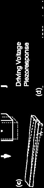
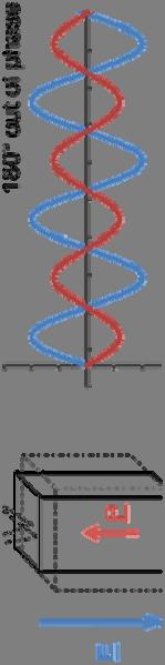
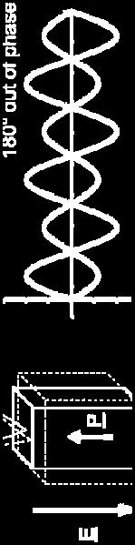
25 Piezo Force Microscopy Dielectrics Piezoelectrics Pyroelectrics Ferroelectrics Ref.: Piezoresponse_Force_Microscopy - Local distribution - Phase: Polarization direction detectable D. Oak Ridge Nat. Labs 25


26 Piezo Force Measurements 3 nm nm 2 1 a.u V -4.2 V Topography Piezo responce Phase polarization value visible two polarization direction - Most HfO 2 grains switchable - PFM serves as base for optimization of film composition D. Martin et al., Adv. Mat. submitted U. Schroeder et al., IWDTF 2013/ and crystallization on simple capacitor structures JJAP
27 Outline 1. Motivation: Ferroelectricity in HfO 2 2. Stabilization of the Ferroelectric HfO 2 Phase 3. Ferroelectric Switching Behavior 4. Device Application: 1T FeFET 5. Summary 27
28 Summary Material: A ferroelectric phase in HfO 2 thin films can be stabilized Ferroelectric phase most likely orthorhombic phase Several stabilizing dopants have been identified Ferroelectric Devices: 1T/1C: FE-HfO 2 adds the 3rd dimension to FRAM scaling World s first 28nm FeFET device HfO 2 -based FeFET added to ITRS roadmap in 2014: Most promising Emerging Memory concept FeFET meets already some DRAM and FLASH specification Superior control of dopant concentration in ALD nanolaminates and usbsequent crystallization of the film is mandatory 28
29 Thank you for your attention This work was supported in part by the EFRE fund of the European Commission within the scope of technology development and in part by the Free State of Saxony (Project: Cool Memory, Heiko, Merlin) and by funding of the Deutsche Forschungs Gemeinschaft(DFG) (Project: Inferox) 29
30 Thanks to the FeFET TEAM: and many more: U. Schröder 1, E. Yurchuk 1, J. Mueller 2, S. Mueller 1, T. Mikolajick 1 T. Boescke 4, D. Martin 1, D. Zhou 1, J. Sundqvist 2, P. Polakowski 2, T. Schenk 1, U. Boettger 5, D. Braeuhaus 5, S. Starschich 5, C. Adelmann 6, M. Popovici 6, T. Schloesser 3, M. Trentzsch 3, M. Goldbach 3, R.v. Bentum 3, S. Knebel 1, T. Olsen 1, R. Hoffmann 2, J. Paul 2, R. Boschke 3, A. Kumar 7, T.M. Arruda 7, S.V. Kalinin 7, M. Alexe 8, A. Morelli 8, A.Kersch 9, R. Maverick
Ferroelectric HfO 2 Thin Films
 Ferroelectric HfO 2 Thin Films May 12 th, 2015 JACKSON ANDERSON ELECTRICAL AND MICROELECTRONIC ENGINEERING ROCHESTER INSTITUTE OF TECHNOLOGY Outline Introduction Background Project Objectives Experimental
Ferroelectric Transistors with Monolayer Molybdenum Disulfide and. Ultra-thin Aluminum-Doped Hafnium Oxide
 Ferroelectric Transistors with Monolayer Molybdenum Disulfide and Ultra-thin Aluminum-Doped Hafnium Oxide Wui Chung Yap 1, Hao Jiang 2, Jialun Liu 1, Qiangfei Xia 2, and Wenjuan Zhu 1 1 Department of Electrical
MaxCaps Next Generation Dielectrics for Integrated Capacitors
 MaxCaps Next Generation Dielectrics for Integrated Capacitors Guenther Ruhl Infineon Technologies AG Σ! 2365 Semicon Europa 2011 Dresden, October 11, 2011 October 11, 2011 1 Outline Introduction MaxCaps
Inductive crystallization effect of atomic-layerdeposited
 Zhang et al. Nanoscale Research Letters (2015) 10:25 DOI 10.1186/s11671-014-0711-4 NANO EXPRESS Open Access Inductive crystallization effect of atomic-layerdeposited Hf 0.5 Zr 0.5 O 2 films for ferroelectric
N ano scale l S il ii lco i n B ased N o nvo lat l i atl ie l M em ory r Chungwoo Kim, Ph.D.
 cw_kim@samsung.com Acknowledgements Collaboration Funding Outline Introduction Current research status Nano fabrication Process Nanoscale patterning SiN thin film Si Nanoparticle Nano devices Nanoscale
Challenges and Opportunities. Prof. J. Raynien Kwo 年
 Nanoelectronics Beyond Si: Challenges and Opportunities Prof. J. Raynien Kwo 年 立 Si CMOS Device Scaling Beyond 22 nm node High κ,, Metal gates, and High mobility channel 1947 First Transistor 1960 1960
Review. Ferroelectric HfO 2 -based materials for next-generation ferroelectric memories
 Review JOURNAL OF ADVANCED DIELECTRICS Vol. 6, No. 2 (2016) 1630003 (11 pages) The Author(s) DOI: 10.1142/S2010135X16300036 Ferroelectric HfO 2 -based materials for next-generation ferroelectric memories
Steep Slope Transistors beyond the Tunnel FET concept. David Esseni, University of Udine
 Steep Slope Transistors beyond the Tunnel FET concept David Esseni, University of Udine Overcome Boltzmann s Tyranny Sub-threshold swing may be expressed as V g = φ s V S/D G In MOSFETs: - second term
Electrical Characterization with SPM Application Modules
 Electrical Characterization with SPM Application Modules Metrology, Characterization, Failure Analysis: Data Storage Magnetoresistive (MR) read-write heads Semiconductor Transistors Interconnect Ferroelectric
Steep-slope WSe 2 Negative Capacitance Field-effect Transistor
 Supplementary Information for: Steep-slope WSe 2 Negative Capacitance Field-effect Transistor Mengwei Si, Chunsheng Jiang, Wonil Chung, Yuchen Du, Muhammad A. Alam, and Peide D. Ye School of Electrical
Chapter 1. Introduction
 Chapter 1. Introduction In this chapter, ferroelectric materials are briefly introduced with emphasis on their nonvolatile memory properties and their potential impact on the current state of digital memories.
Pyroelectric Response in Crystalline Hafnium Zirconium Oxide (Hf 1-x Zr x O 2 ) Thin Films
 Thin Films") Pyroelectric Response in Crystalline Hafnium Zirconium Oxide (Hf 1-x Zr x O 2 ) Thin Films S. W. Smith, 1 A. R. Kitahara, 1, a) M. A. Rodriguez, 1 M. D. Henry, 1 M. T. Brumbach, 1 J. F. 1, b) Ihlefeld
Pyroelectric Response in Crystalline Hafnium Zirconium Oxide (Hf 1-x Zr x O 2 ) Thin Films S. W. Smith, 1 A. R. Kitahara, 1, a) M. A. Rodriguez, 1 M. D. Henry, 1 M. T. Brumbach, 1 J. F. 1, b) Ihlefeld
Multiple Gate CMOS and Beyond
 Multiple CMOS and Beyond Dept. of EECS, KAIST Yang-Kyu Choi Outline 1. Ultimate Scaling of MOSFETs - 3nm Nanowire FET - 8nm Non-Volatile Memory Device 2. Multiple Functions of MOSFETs 3. Summary 2 CMOS
Gold Nanoparticles Floating Gate MISFET for Non-Volatile Memory Applications
 Gold Nanoparticles Floating Gate MISFET for Non-Volatile Memory Applications D. Tsoukalas, S. Kolliopoulou, P. Dimitrakis, P. Normand Institute of Microelectronics, NCSR Demokritos, Athens, Greece S. Paul,
Electrical and Reliability Characteristics of RRAM for Cross-point Memory Applications. Hyunsang Hwang
 Electrical and Reliability Characteristics of RRAM for Cross-point Memory Applications Hyunsang Hwang Dept. of Materials Science and Engineering Gwangju Institute of Science and Technology (GIST), KOREA
New Ferroelectric Material for Embedded FRAM LSIs
 New Ferroelectric Material for Embedded FRAM LSIs V Kenji Maruyama V Masao Kondo V Sushil K. Singh V Hiroshi Ishiwara (Manuscript received April 5, 2007) The strong growth of information network infrastructures
How a single defect can affect silicon nano-devices. Ted Thorbeck
 How a single defect can affect silicon nano-devices Ted Thorbeck tedt@nist.gov The Big Idea As MOS-FETs continue to shrink, single atomic scale defects are beginning to affect device performance Gate Source
Design and Simulation of Short Channel Si:HfO2 Ferroelectric Field Effect Transistor (FeFET)
") Rochester Institute of Technology RIT Scholar Works Theses Thesis/Dissertation Collections 8-15-2014 Design and Simulation of Short Channel Si:HfO2 Ferroelectric Field Effect Transistor (FeFET) Idris H.
Rochester Institute of Technology RIT Scholar Works Theses Thesis/Dissertation Collections 8-15-2014 Design and Simulation of Short Channel Si:HfO2 Ferroelectric Field Effect Transistor (FeFET) Idris H.
Low Frequency Noise in MoS 2 Negative Capacitance Field-effect Transistor
 Low Frequency Noise in MoS Negative Capacitance Field-effect Transistor Sami Alghamdi, Mengwei Si, Lingming Yang, and Peide D. Ye* School of Electrical and Computer Engineering Purdue University West Lafayette,
Frequency dispersion effect and parameters. extraction method for novel HfO 2 as gate dielectric
 048 SCIENCE CHINA Information Sciences April 2010 Vol. 53 No. 4: 878 884 doi: 10.1007/s11432-010-0079-8 Frequency dispersion effect and parameters extraction method for novel HfO 2 as gate dielectric LIU
Influence of electrode materials on CeO x based resistive switching
 Influence of electrode materials on CeO x based resistive switching S. Kano a, C. Dou a, M. Hadi a, K. Kakushima b, P. Ahmet a, A. Nishiyama b, N. Sugii b, K. Tsutsui b, Y. Kataoka b, K. Natori a, E. Miranda
Supplementary Information for. Non-volatile memory based on ferroelectric photovoltaic effect
 Supplementary Information for Non-volatile memory based on ferroelectric photovoltaic effect Rui Guo 1, Lu You 1, Yang Zhou 1, Zhi Shiuh Lim 1, Xi Zou 1, Lang Chen 1, R. Ramesh 2, Junling Wang 1* 1 School
Moores Law for DRAM. 2x increase in capacity every 18 months 2006: 4GB
 MEMORY Moores Law for DRAM 2x increase in capacity every 18 months 2006: 4GB Corollary to Moores Law Cost / chip ~ constant (packaging) Cost / bit = 2X reduction / 18 months Current (2008) ~ 1 micro-cent
A Ferroelectric Semiconductor Field-Effect Transistor
 A Ferroelectric Semiconductor Field-Effect Transistor Mengwei Si 1,4, Shengjie Gao 2,4, Gang Qiu 1,4, Jingkai Qin 1,4, Yuqin Duan 1,4, Jie Jian 3, Haiyan Wang 3, Wenzhuo Wu 2,4 and Peide D. Ye 1,4, * 1
ECE 340 Lecture 39 : MOS Capacitor II
 ECE 340 Lecture 39 : MOS Capacitor II Class Outline: Effects of Real Surfaces Threshold Voltage MOS Capacitance-Voltage Analysis Things you should know when you leave Key Questions What are the effects
A final review session will be offered on Thursday, May 10 from 10AM to 12noon in 521 Cory (the Hogan Room).
.") A final review session will be offered on Thursday, May 10 from 10AM to 12noon in 521 Cory (the Hogan Room). The Final Exam will take place from 12:30PM to 3:30PM on Saturday May 12 in 60 Evans.» All of
A final review session will be offered on Thursday, May 10 from 10AM to 12noon in 521 Cory (the Hogan Room). The Final Exam will take place from 12:30PM to 3:30PM on Saturday May 12 in 60 Evans.» All of
JUNCTION LEAKAGE OF A SiC-BASED NON-VOLATILE RANDOM ACCESS MEMORY (NVRAM) K. Y. Cheong ABSTRACT INTRODUCTION
 K. Y. Cheong ABSTRACT INTRODUCTION") JUNCTION LEAKAGE OF A SiC-BASED NON-VOLATILE RANDOM ACCESS MEMORY (NVRAM) K. Y. Cheong Electronic Materials Research Group, School of Materials and Mineral Resources Engineering, Engineering Campus, Universiti
JUNCTION LEAKAGE OF A SiC-BASED NON-VOLATILE RANDOM ACCESS MEMORY (NVRAM) K. Y. Cheong Electronic Materials Research Group, School of Materials and Mineral Resources Engineering, Engineering Campus, Universiti
Negative-Bias Temperature Instability (NBTI) of GaN MOSFETs
 of GaN MOSFETs") Negative-Bias Temperature Instability (NBTI) of GaN MOSFETs Alex Guo and Jesús A. del Alamo Microsystems Technology Laboratories (MTL) Massachusetts Institute of Technology (MIT) Cambridge, MA, USA Sponsor:
Negative-Bias Temperature Instability (NBTI) of GaN MOSFETs Alex Guo and Jesús A. del Alamo Microsystems Technology Laboratories (MTL) Massachusetts Institute of Technology (MIT) Cambridge, MA, USA Sponsor:
An interfacial investigation of high-dielectric constant material hafnium oxide on Si substrate B
 Thin Solid Films 488 (2005) 167 172 www.elsevier.com/locate/tsf An interfacial investigation of high-dielectric constant material hafnium oxide on Si substrate B S.C. Chen a, T, J.C. Lou a, C.H. Chien
Recent Development of FinFET Technology for CMOS Logic and Memory
 Recent Development of FinFET Technology for CMOS Logic and Memory Chung-Hsun Lin EECS Department University of California at Berkeley Why FinFET Outline FinFET process Unique features of FinFET Mobility,
Quantum Mechanical Simulation for Ultra-thin High-k Gate Dielectrics Metal Oxide Semiconductor Field Effect Transistors
 Mechanical Simulation for Ultra-thin High-k Gate Dielectrics Metal Oxide Semiconductor Field Effect Transistors Shih-Ching Lo 1, Yiming Li 2,3, and Jyun-Hwei Tsai 1 1 National Center for High-Performance
CHAPTER-1 INTRODUCTION
 CHAPTER-1 INTRODUCTION 1.1 OVERVIEW In today s microelectronics computer industry, various types of memories are used for the data storage. Generally, memories are categorized into volatile and non-volatile.
Low leakage ZrO 2 based capacitors for sub 20 nm DRAM technology nodes
 Low leakage ZrO 2 based capacitors for sub 20 nm DRAM technology nodes Milan Pešić, 1 Steve Knebel, 1 Maximilian Geyer, 1 Sebastian Schmelzer 2, Ulrich Böttger 2, Nadiia Kolomiiets 3, Valeri V. Afanas
Characterization of Charge Trapping and Dielectric Breakdown of HfAlOx/SiON Dielectric Gate Stack
 Characterization of Charge Trapping and Dielectric Breakdown of HfAlOx/SiON Dielectric Gate Stack Y. Pei, S. Nagamachi, H. Murakami, S. Higashi, S. Miyazaki, T. Kawahara and K. Torii Graduate School of
Stretching the Barriers An analysis of MOSFET Scaling. Presenters (in order) Zeinab Mousavi Stephanie Teich-McGoldrick Aseem Jain Jaspreet Wadhwa
 Zeinab Mousavi Stephanie Teich-McGoldrick Aseem Jain Jaspreet Wadhwa") Stretching the Barriers An analysis of MOSFET Scaling Presenters (in order) Zeinab Mousavi Stephanie Teich-McGoldrick Aseem Jain Jaspreet Wadhwa Why Small? Higher Current Lower Gate Capacitance Higher
Stretching the Barriers An analysis of MOSFET Scaling Presenters (in order) Zeinab Mousavi Stephanie Teich-McGoldrick Aseem Jain Jaspreet Wadhwa Why Small? Higher Current Lower Gate Capacitance Higher
Laser Annealing of MOCVD Deposited Ferroelectric SrBi 2 Ta 2 O 9, Pb(Zr X Ti 1-X )O 3 and CeMnO 3 Thin Films
O 3 and CeMnO 3 Thin Films") 1 Laser Annealing of MOCVD Deposited Ferroelectric SrBi 2 Ta 2 O 9, Pb(Zr X Ti 1-X )O 3 and CeMnO 3 Thin Films N.M. Sbrockey 1, J.D. Cuchiaro 1, L.G. Provost 1, C.E. Rice 1, S. Sun 1, G.S. Tompa 1, R.L.
1 Laser Annealing of MOCVD Deposited Ferroelectric SrBi 2 Ta 2 O 9, Pb(Zr X Ti 1-X )O 3 and CeMnO 3 Thin Films N.M. Sbrockey 1, J.D. Cuchiaro 1, L.G. Provost 1, C.E. Rice 1, S. Sun 1, G.S. Tompa 1, R.L.
Floating Gate Devices: Operation and Compact Modeling
 Floating Gate Devices: Operation and Compact Modeling Paolo Pavan (1), Luca Larcher (1) and Andrea MarmirolI (2) (1) Università di Modena e Reggio Emilia, Via Fogliani, 1 42100 Reggio Emilia (Italy) -
Vanadium Dioxide (VO 2 ) is also a Ferroelectric: Properties from Memory Structures
 is also a Ferroelectric: Properties from Memory Structures") 211 11th IEEE International Conference on Nanotechnology Portland Marriott August 15-18, 211, Portland, Oregon, USA Vanadium Dioxide (VO 2 ) is also a Ferroelectric: Properties from Memory Structures S.
211 11th IEEE International Conference on Nanotechnology Portland Marriott August 15-18, 211, Portland, Oregon, USA Vanadium Dioxide (VO 2 ) is also a Ferroelectric: Properties from Memory Structures S.
CVD: General considerations.
 CVD: General considerations. PVD: Move material from bulk to thin film form. Limited primarily to metals or simple materials. Limited by thermal stability/vapor pressure considerations. Typically requires
NRAM: High Performance, Highly Reliable Emerging Memory
 NRAM: High Performance, Highly Reliable Emerging Memory Sheyang Ning,2, Tomoko Ogura Iwasaki, Darlene Viviani 2, Henry Huang 2, Monte Manning 2, Thomas Rueckes 2, Ken Takeuchi Chuo University 2 Nantero
ESE 570: Digital Integrated Circuits and VLSI Fundamentals
 ESE 570: Digital Integrated Circuits and VLSI Fundamentals Lec 4: January 29, 2019 MOS Transistor Theory, MOS Model Penn ESE 570 Spring 2019 Khanna Lecture Outline! CMOS Process Enhancements! Semiconductor
Reliability and Instability of GaN MIS-HEMTs for Power Electronics
 Reliability and Instability of GaN MIS-HEMTs for Power Electronics Jesús A. del Alamo, Alex Guo and Shireen Warnock Microsystems Technology Laboratories Massachusetts Institute of Technology 2016 Fall
Defects in Semiconductors
 Defects in Semiconductors Mater. Res. Soc. Symp. Proc. Vol. 1370 2011 Materials Research Society DOI: 10.1557/opl.2011. 771 Electronic Structure of O-vacancy in High-k Dielectrics and Oxide Semiconductors
Lecture 15 OUTLINE. MOSFET structure & operation (qualitative) Review of electrostatics The (N)MOS capacitor
 Review of electrostatics The (N)MOS capacitor") Lecture 15 OUTLINE MOSFET structure & operation (qualitative) Review of electrostatics The (N)MOS capacitor Electrostatics t ti Charge vs. voltage characteristic Reading: Chapter 6.1 6.2.1 EE105 Fall 2007
Lecture 15 OUTLINE MOSFET structure & operation (qualitative) Review of electrostatics The (N)MOS capacitor Electrostatics t ti Charge vs. voltage characteristic Reading: Chapter 6.1 6.2.1 EE105 Fall 2007
Ferroelectricity in yttrium-doped hafnium oxide
 Ferroelectricity in yttrium-doped hafnium oxide J. Müller, U. Schröder, T. S. Böscke, I. Müller, U. Böttger et al. Citation: J. Appl. Phys. 110, 114113 (2011); doi: 10.1063/1.3667205 View online: http://dx.doi.org/10.1063/1.3667205
During such a time interval, the MOS is said to be in "deep depletion" and the only charge present in the semiconductor is the depletion charge.
 Q1 (a) If we apply a positive (negative) voltage step to a p-type (n-type) MOS capacitor, which is sufficient to generate an inversion layer at equilibrium, there is a time interval, after the step, when
Supporting Information for: Sustained sub-60 mv/decade switching via the negative capacitance effect in MoS 2 transistors
 Supporting Information for: Sustained sub-60 mv/decade switching via the negative capacitance effect in MoS 2 transistors Felicia A. McGuire 1, Yuh-Chen Lin 1, Katherine Price 1, G. Bruce Rayner 2, Sourabh
Analysis of Band-to-band. Tunneling Structures. Title of Talk. Dimitri Antoniadis and Judy Hoyt (PIs) Jamie Teherani and Tao Yu (Students) 8/21/2012
 Jamie Teherani and Tao Yu (Students) 8/21/2012") 1 Analysis of Band-to-band Title of Talk Tunneling Structures Dimitri Antoniadis and Judy Hoyt (PIs) Jamie Teherani and Tao Yu (Students) 8/21/2012 A Science & Technology Center Vertical Type-II TFET Structure
1 Analysis of Band-to-band Title of Talk Tunneling Structures Dimitri Antoniadis and Judy Hoyt (PIs) Jamie Teherani and Tao Yu (Students) 8/21/2012 A Science & Technology Center Vertical Type-II TFET Structure
High Dielectric Constant (k) Materials
 Materials") Part 6: High Dielectric Constant (k), Gate Electrode, & Channel Materials O 2 gate ide is approaching physical limits Thickness & Current M O S poly-crystalline V Source W Source Contact Insulator n +
Part 6: High Dielectric Constant (k), Gate Electrode, & Channel Materials O 2 gate ide is approaching physical limits Thickness & Current M O S poly-crystalline V Source W Source Contact Insulator n +
Lecture 12: MOS Capacitors, transistors. Context
 Lecture 12: MOS Capacitors, transistors Context In the last lecture, we discussed PN diodes, and the depletion layer into semiconductor surfaces. Small signal models In this lecture, we will apply those
Mechanism of Switching and Related Challenges in Transition Metal Oxide Based RRAM Devices
 Mechanism of Switching and Related Challenges in Transition Metal Oxide Based RRAM Devices Rashmi Jha and Branden Long Dept. of Electrical Engineering and Computer Science University of Toledo Toledo,
Gate Carrier Injection and NC-Non- Volatile Memories
 Gate Carrier Injection and NC-Non- Volatile Memories Jean-Pierre Leburton Department of Electrical and Computer Engineering and Beckman Institute University of Illinois at Urbana-Champaign Urbana, IL 61801,
A Universal Memory Model for Design Exploration. Ketul Sutaria, Chi-Chao Wang, Yu (Kevin) Cao School of ECEE, ASU
 Cao School of ECEE, ASU") A Universal Memory Model for Design Exploration Ketul Sutaria, Chi-Chao Wang, Yu (Kevin) Cao School of ECEE, ASU Universal Memory Modeling because there is no universal memory device! Modeling needs in
A Universal Memory Model for Design Exploration Ketul Sutaria, Chi-Chao Wang, Yu (Kevin) Cao School of ECEE, ASU Universal Memory Modeling because there is no universal memory device! Modeling needs in
Magnetic core memory (1951) cm 2 ( bit)
 cm 2 ( bit)") Magnetic core memory (1951) 16 16 cm 2 (128 128 bit) Semiconductor Memory Classification Read-Write Memory Non-Volatile Read-Write Memory Read-Only Memory Random Access Non-Random Access EPROM E 2 PROM
Magnetic core memory (1951) 16 16 cm 2 (128 128 bit) Semiconductor Memory Classification Read-Write Memory Non-Volatile Read-Write Memory Read-Only Memory Random Access Non-Random Access EPROM E 2 PROM
This is the author s final accepted version.
 Al-Ameri, T., Georgiev, V.P., Adamu-Lema, F. and Asenov, A. (2017) Does a Nanowire Transistor Follow the Golden Ratio? A 2D Poisson- Schrödinger/3D Monte Carlo Simulation Study. In: 2017 International
R&D Issues for High-k Gate Dielectrics
 R&D Issues for High-k Gate Dielectrics T.P. Ma Yale University Spacer High-k Gate Dielectric Stack Source Drain Gate electrode, poly Upper interfacial region Bulk high-k film Lower interfacial region Substrate
Computational Science Studies toward Future Nano-Devices. Kenji Shiraishi. University of Tsukuba
 Computational Science Studies toward Future Nano-Devices Kenji Shiraishi University of Tsukuba 1 1. Introduction Contents 2. Key physics in ionic materials obtained by computational sciences. 3. Operation
3D Stacked Buck Converter with SrTiO 3 (STO) Capacitors on Silicon Interposer
 Capacitors on Silicon Interposer") 3D Stacked Buck Converter with SrTiO 3 (STO) Capacitors on Silicon Interposer Makoto Takamiya 1, Koichi Ishida 1, Koichi Takemura 2,3, and Takayasu Sakurai 1 1 University of Tokyo, Japan 2 NEC Corporation,
3D Stacked Buck Converter with SrTiO 3 (STO) Capacitors on Silicon Interposer Makoto Takamiya 1, Koichi Ishida 1, Koichi Takemura 2,3, and Takayasu Sakurai 1 1 University of Tokyo, Japan 2 NEC Corporation,
J. Price, 1,2 Y. Q. An, 1 M. C. Downer 1 1 The university of Texas at Austin, Department of Physics, Austin, TX
 Understanding process-dependent oxygen vacancies in thin HfO 2 /SiO 2 stacked-films on Si (100) via competing electron-hole injection dynamic contributions to second harmonic generation. J. Price, 1,2
Agenda. 1. Atomic Layer Deposition Technology
 Agenda 1. Atomic Layer Deposition Technology 2. What is ALD? Atomic Layer Deposition is invented in 1977 by T. Suntola et al. - New Deposition Method for Electro-Luminescent Display (ZnS:Mn Thin Films)
MODELING OF CV CHARACTERISTICS OF HIGH-k MIM CAPACITORS
 Chapter 6 MODELING OF CV CHARACTERISTICS OF HIGH-k MIM CAPACITORS 6.1 Introduction and Motivation Capacitance-Voltage characteristics and voltage linearity of MIM capacitor are important performance parameters
Electronics with 2D Crystals: Scaling extender, or harbinger of new functions?
 Electronics with 2D Crystals: Scaling extender, or harbinger of new functions? 1 st Workshop on Data Abundant Systems Technology Stanford, April 2014 Debdeep Jena (djena@nd.edu) Electrical Engineering,
Control of Flat Band Voltage by Partial Incorporation of La 2 O 3 or Sc 2 O 3 into HfO 2 in Metal/HfO 2 /SiO 2 /Si MOS Capacitors
 Control of Flat Band Voltage by Partial Incorporation of La 2 O 3 or Sc 2 O 3 into HfO 2 in Metal/HfO 2 /SiO 2 /Si MOS Capacitors M. Adachi 1, K. Okamoto 1, K. Kakushima 2, P. Ahmet 1, K. Tsutsui 2, N.
CURRICULUM VITAE HUAMIN LI UPDATED: DECEMBER 1, 2015 MAIN RESEARCH INTERESTS EDUCATION
 CURRICULUM VITAE HUAMIN LI UPDATED: DECEMBER 1, 2015 Postdoctoral Research Associate Center for Low Energy Systems Technology (LEAST), Department of Electrical Engineering University of Notre Dame, B20
Improved Interfacial and Electrical Properties of GaSb Metal Oxide
 Improved Interfacial and Electrical Properties of GaSb Metal Oxide Semiconductor Devices Passivated with Acidic (NH 4 ) 2 S Solution Lianfeng Zhao, Zhen Tan, Jing Wang, and Jun Xu * Tsinghua National Laboratory
Extrinsic and Intrinsic Frequency Dispersion of High-k Materials in Capacitance-Voltage Measurements
 Materials 01, 5, 1005-103; doi:10.3390/ma5061005 Review OPEN ACCESS materials ISSN 1996-1944 www.mdpi.com/journal/materials Extrinsic and Intrinsic Frequency Dispersion of High-k Materials in Capacitance-Voltage
Advanced Flash and Nano-Floating Gate Memories
 Advanced Flash and Nano-Floating Gate Memories Mater. Res. Soc. Symp. Proc. Vol. 1337 2011 Materials Research Society DOI: 10.1557/opl.2011.1028 Scaling Challenges for NAND and Replacement Memory Technology
The Pennsylvania State University. Kurt J. Lesker Company. North Carolina State University. Taiwan Semiconductor Manufacturing Company 1
 Enhancement Mode Strained (1.3%) Germanium Quantum Well FinFET (W fin =20nm) with High Mobility (μ Hole =700 cm 2 /Vs), Low EOT (~0.7nm) on Bulk Silicon Substrate A. Agrawal 1, M. Barth 1, G. B. Rayner
Chapter 3 Basics Semiconductor Devices and Processing
 Chapter 3 Basics Semiconductor Devices and Processing Hong Xiao, Ph. D. www2.austin.cc.tx.us/hongxiao/book.htm Hong Xiao, Ph. D. www2.austin.cc.tx.us/hongxiao/book.htm 1 Objectives Identify at least two
Enhanced Mobility CMOS
 Enhanced Mobility CMOS Judy L. Hoyt I. Åberg, C. Ni Chléirigh, O. Olubuyide, J. Jung, S. Yu, E.A. Fitzgerald, and D.A. Antoniadis Microsystems Technology Laboratory MIT, Cambridge, MA 02139 Acknowledge
ALD high-k and higher-k integration on GaAs
 ALD high-k and higher-k integration on GaAs Ozhan Koybasi 1), Min Xu 1), Yiqun Liu 2), Jun-Jieh Wang 2), Roy G. Gordon 2), and Peide D. Ye 1)* 1) School of Electrical and Computer Engineering, Purdue University,
Scaling up Chemical Vapor Deposition Graphene to 300 mm Si substrates
 Scaling up Chemical Vapor Deposition Graphene to 300 mm Si substrates Co- Authors Aixtron Alex Jouvray Simon Buttress Gavin Dodge Ken Teo The work shown here has received partial funding from the European
Experimental and Theoretical Study of Electrode Effects in HfO2 based RRAM
 Experimental and Theoretical Study of Electrode Effects in HfO2 based RRAM C. Cagli 1, J. Buckley 1, V. Jousseaume 1, T. Cabout 1, A. Salaun 1, H. Grampeix 1, J. F. Nodin 1,H. Feldis 1, A. Persico 1, J.
Thin Film Transistors (TFT)
") Thin Film Transistors (TFT) a-si TFT - α-si:h (Hydrogenated amorphous Si) deposited with a PECVD system (low temp. process) replaces the single crystal Si substrate. - Inverted staggered structure with
Thin Film Transistors (TFT) a-si TFT - α-si:h (Hydrogenated amorphous Si) deposited with a PECVD system (low temp. process) replaces the single crystal Si substrate. - Inverted staggered structure with
Effective Capacitance Enhancement Methods for 90-nm DRAM Capacitors
 Journal of the Korean Physical Society, Vol. 44, No. 1, January 2004, pp. 112 116 Effective Capacitance Enhancement Methods for 90-nm DRAM Capacitors Y. K. Park, Y. S. Ahn, S. B. Kim, K. H. Lee, C. H.
Carbon Nanotubes in Interconnect Applications
 Carbon Nanotubes in Interconnect Applications Page 1 What are Carbon Nanotubes? What are they good for? Why are we interested in them? - Interconnects of the future? Comparison of electrical properties
Carbon Nanotubes for Interconnect Applications Franz Kreupl, Andrew P. Graham, Maik Liebau, Georg S. Duesberg, Robert Seidel, Eugen Unger
 Carbon Nanotubes for Interconnect Applications Franz Kreupl, Andrew P. Graham, Maik Liebau, Georg S. Duesberg, Robert Seidel, Eugen Unger Infineon Technologies Corporate Research Munich, Germany Outline
Digital Integrated Circuits A Design Perspective
 Semiconductor Memories Adapted from Chapter 12 of Digital Integrated Circuits A Design Perspective Jan M. Rabaey et al. Copyright 2003 Prentice Hall/Pearson Outline Memory Classification Memory Architectures
Plasma-Surface Interactions in Patterning High-k k Dielectric Materials
 Plasma-Surface Interactions in Patterning High-k k Dielectric Materials October 11, 4 Feature Level Compensation and Control Seminar Jane P. Chang Department of Chemical Engineering University of California,
ESE 570: Digital Integrated Circuits and VLSI Fundamentals
 ESE 570: Digital Integrated Circuits and VLSI Fundamentals Lec 4: January 23, 2018 MOS Transistor Theory, MOS Model Penn ESE 570 Spring 2018 Khanna Lecture Outline! CMOS Process Enhancements! Semiconductor
RECENTLY, (Ba, Sr)TiO thin films have been intensively
TiO thin films have been intensively") 342 IEEE TRANSACTIONS ON ELECTRON DEVICES, VOL. 46, NO. 2, FEBRUARY 1999 Impact of Time Dependent Dielectric Breakdown and Stress-Induced Leakage Current on the Reliability of High Dielectric Constant
342 IEEE TRANSACTIONS ON ELECTRON DEVICES, VOL. 46, NO. 2, FEBRUARY 1999 Impact of Time Dependent Dielectric Breakdown and Stress-Induced Leakage Current on the Reliability of High Dielectric Constant
! CMOS Process Enhancements. ! Semiconductor Physics. " Band gaps. " Field Effects. ! MOS Physics. " Cut-off. " Depletion.
 ESE 570: Digital Integrated Circuits and VLSI Fundamentals Lec 4: January 9, 019 MOS Transistor Theory, MOS Model Lecture Outline CMOS Process Enhancements Semiconductor Physics Band gaps Field Effects
Lecture 15 OUTLINE. MOSFET structure & operation (qualitative) Review of electrostatics The (N)MOS capacitor
 Review of electrostatics The (N)MOS capacitor") Lecture 15 OUTLINE MOSFET structure & operation (qualitative) Review of electrostatics The (N)MOS capacitor Electrostatics Charge vs. voltage characteristic Reading: Chapter 6.1 6.2.1 EE15 Spring 28 Lecture
Lecture 15 OUTLINE MOSFET structure & operation (qualitative) Review of electrostatics The (N)MOS capacitor Electrostatics Charge vs. voltage characteristic Reading: Chapter 6.1 6.2.1 EE15 Spring 28 Lecture
Supporting Information
 Supporting Information Monolithically Integrated Flexible Black Phosphorus Complementary Inverter Circuits Yuanda Liu, and Kah-Wee Ang* Department of Electrical and Computer Engineering National University
3D capacitors on silicon with high density pore network and ZrO2 dielectric films deposited by MOCVD
 3D capacitors on silicon with high density pore network and ZrO2 dielectric films deposited by MOCVD Magali Brunet 1, Gérald Leclerc 1, Emmanuel Scheid 1, Jean- Louis Sanchez 1 1 LAAS-CNRS, University
Self-study problems and questions Processing and Device Technology, FFF110/FYSD13
 Self-study problems and questions Processing and Device Technology, FFF110/FYSD13 Version 2016_01 In addition to the problems discussed at the seminars and at the lectures, you can use this set of problems
DKDT: A Performance Aware Dual Dielectric Assignment for Tunneling Current Reduction
 DKDT: A Performance Aware Dual Dielectric Assignment for Tunneling Current Reduction Saraju P. Mohanty Dept of Computer Science and Engineering University of North Texas smohanty@cs.unt.edu http://www.cs.unt.edu/~smohanty/
AN ABSTRACT OF THE THESIS OF
 AN ABSTRACT OF THE THESIS OF Santosh Murali for the degree of Master of Science in Electrical and Computer Engineering presented on December 20, 2011. Title: Investigation of Bipolar Resistive Switching
Optimization of the Dielectric Constant of a Blocking Dielectric in the Nonvolatile Memory Based on Silicon Nitride
 ISSN 8756-699, Optoelectronics, Instrumentation and Data Processing, 9, Vol. 45, No. 4, pp. 48 5. c Allerton Press, Inc., 9. Original Russian Text c Y. N. Novikov, V. A. Gritsenko, K. A. Nasyrov, 9, published
Electric-Field Induced F - Migration in Self-Aligned InGaAs MOSFETs and Mitigation
 Electric-Field Induced F - Migration in Self-Aligned InGaAs MOSFETs and Mitigation X. Cai, J. Lin, D. A. Antoniadis and J. A. del Alamo Microsystems Technology Laboratories, MIT December 5, 2016 Sponsors:
Lecture 6 PN Junction and MOS Electrostatics(III) Metal-Oxide-Semiconductor Structure
 Metal-Oxide-Semiconductor Structure") Lecture 6 PN Junction and MOS Electrostatics(III) Metal-Oxide-Semiconductor Structure Outline 1. Introduction to MOS structure 2. Electrostatics of MOS in thermal equilibrium 3. Electrostatics of MOS with
Lecture 6 PN Junction and MOS Electrostatics(III) Metal-Oxide-Semiconductor Structure Outline 1. Introduction to MOS structure 2. Electrostatics of MOS in thermal equilibrium 3. Electrostatics of MOS with
Comparative studies of Ge and Si p-channel metal oxide semiconductor field-effect-transistors with HfSiON dielectric and TaN metal gate
 Comparative studies of Ge and Si p-channel metal oxide semiconductor field-effect-transistors with HfSiON dielectric and TaN metal gate Hu Ai-Bin( 胡爱斌 ) and Xu Qiu-Xia( 徐秋霞 ) Institute of Microelectronics,
FLCC Seminar. Spacer Lithography for Reduced Variability in MOSFET Performance
 1 Seminar Spacer Lithography for Reduced Variability in MOSFET Performance Prof. Tsu-Jae King Liu Electrical Engineering & Computer Sciences Dept. University of California at Berkeley Graduate Student:
High tunable dielectric response of Pb 0.87 Ba 0.1 La 0.02 (Zr 0.6 Sn 0.33 Ti 0.07 ) O 3 thin film
 O 3 thin film") Journal of Applied Physics, 2010, Volume 108, Issue 4, paper number 044107 High tunable dielectric response of Pb 0.87 Ba 0.1 La 0.02 (Zr 0.6 Sn 0.33 Ti 0.07 ) O 3 thin film T. M. Correia and Q. Zhang*
Journal of Applied Physics, 2010, Volume 108, Issue 4, paper number 044107 High tunable dielectric response of Pb 0.87 Ba 0.1 La 0.02 (Zr 0.6 Sn 0.33 Ti 0.07 ) O 3 thin film T. M. Correia and Q. Zhang*
Part 4: Heterojunctions - MOS Devices. MOSFET Current Voltage Characteristics
 MOS Device Uses: Part 4: Heterojunctions - MOS Devices MOSCAP capacitor: storing charge, charge-coupled device (CCD), etc. MOSFET transistor: switch, current amplifier, dynamic random access memory (DRAM-volatile),
Ferroelectric Field-Effect Transistors Based on MoS 2 and
 Supplementary Information for: Ferroelectric Field-Effect Transistors Based on MoS 2 and CuInP 2 S 6 Two-Dimensional Van der Waals Heterostructure Mengwei Si, Pai-Ying Liao, Gang Qiu, Yuqin Duan, and Peide
5. Building Blocks I: Ferroelectric inorganic micro- and nano(shell) tubes
 tubes") 5. Building Blocks I: Ferroelectric inorganic micro- and nano(shell) tubes 5.1 New candidates for nanoelectronics: ferroelectric nanotubes In this chapter, one of the core elements for a complex building
5. Building Blocks I: Ferroelectric inorganic micro- and nano(shell) tubes 5.1 New candidates for nanoelectronics: ferroelectric nanotubes In this chapter, one of the core elements for a complex building
Si Based Mis Devices with Ferroelectric Polymer Films for Non-Volatile Memory Applications
 University of Massachusetts Amherst ScholarWorks@UMass Amherst Masters Theses 1911 - February 2014 January 2007 Si Based Mis Devices with Ferroelectric Polymer Films for Non-Volatile Memory Applications
Nanocarbon Interconnects - From 1D to 3D
 Nanocarbon Interconnects - From 1D to 3D Cary Y. Yang Santa Clara University Outline Introduction CNT as 1D interconnect structure CNT-graphene as all-carbon 3D interconnect Summary Device Scaling driven
On the Ferroelectric Polarization Switching of Hafnium. Zirconium Oxide in Ferroelectric/Dielectric Stack
 On the Ferroelectric Polarization Switching of Hafnium Zirconium Oxide in Ferroelectric/Dielectric Stack Mengwei Si, Xiao Lyu, and Peide D. Ye School of Electrical and Computer Engineering and Birck Nanotechnology