Indian Institute of Technology Kanpur
|
|
|
- Helena Ramsey
- 5 years ago
- Views:
Transcription


1 Indian Institute of Technology Kanpur Nano-Science & Technology Initiative Department of Science and Technology, India Ashutosh Sharma Department of Chemical Engineering
2 DST Unit on IITK Mesoscale Structures, Patterning and Properties with Emphasis on Soft Materials and Thin Films A state-of-the-art facility and resources for soft matter nanoscience and nanotechnology. Explore new techniques of nano-fabrication based on a creative combination of top-down including soft lithography, self-assembly and selforganization. Projects related to nano-scale understanding, fabrication and use of soft materials in coatings, NEMS, functional interfaces and bulk-nano


3 Journey of the last two years!


4 Nano-Sciences at IITK: A Mega-Passion. ructure Property Behavior Micro- and Nano Fab Lithographies, Beams Self-assembly p- wn Bottom-up Self-organization
5 Highly Multidisciplinary AND Interdisciplinary Team CORE GROUP FACULTY (~ 10) Ashutosh Sharma (soft nano fabrication; nanomechanics) Ramesh C. Budhani (magnetic nanomaterials; spintronics) V. N. Kulkarni (ion beams; fabrication) Department of Chemical Engineering Animangsu Ghatak (microfluidics; soft fabrication) Yogesh Joshi (polymer-clay nanocomposites) Nishith Verma (carbon nanocomposites) Jayant K. Singh (simulations of soft materials)
6 Department of Chemistry Sandeep Verma (self-assembly; nano-bio) Department of Materials and Metallurgical Engineering Ashish Garg (thin films; nano-structures) Department of Mechanical Engineering Shantanu Bhatacharya (nano-fabrication; MEMS) Department of Physics Rajiv Gupta (SPM; Raman) (Additional members may be co-opted depending on the focus of research---soft materials based patterning and their expertise in the Unit resources)
7 Major Facilities at Nanosciences Center About 2500 sq. ft. of class clean rooms Fabrication resources Characterization resources Collaborations: Northwestern; UIUC; UCI; Cambridge; NIST; JNCASR; IISc. Fall 2007
8 Fabrication Focused Ion Beam (Dual Beam FIB) E-Beam Lithography Broad Beam Ion Mill Maskless Photolithography Pulse laser Coating Langmuir-Blodgett Deposition NSOM UV Lithography Nanoimprint Lithography Polymer Ink-jet Printing High temperature furnaces..
 SEM WAXRD; SAX SQUID Optical Microscopes Contact Angle")
9 Characterization Confocal Microscopy Micro-Raman Scanning Probe Microscopies Near-field Scanning Optical Microscopy (NSOM) Imaging and Spectroscopic Ellipsometry Profilometers (Mechanical and Optical) SEM WAXRD; SAX SQUID Optical Microscopes Contact Angle Goniometer..
10 Specific Scientific Objectives: Development of novel and facile techniques for patterning, structuring and fabrication using soft materials like polymers, gels, biological materials Development of functional interfaces such as superhydrophobic surfaces and super adhesives based on meso patterning of surfaces Attachment detachment energetics of sub-micron particles to surface and modulation by surfactants Synthesis of ordered arrays of quantum dots and nanowires including doped oxide and metal alloys and magnetic materials
11 Exploration of interfacial instabilities and failure mechanism in soft nano-structures Development of soft composites including polymernanoclay composites, thin film of meso-porous silica and its nano composites Magnetic nano particles and assemblies Development of computational nanomechanics Micro-SQUIDS and nanoscale magnetics including magnetic relaxation and supermagnetism Fabrication of carbon meso-structures based on soft fabrication techniques Microfluidic based devices and sensors
12 Current Areas of Nanosciences at IITK Fabrication using FIB, E-beam (masters; devices ) Novel soft-lithographies for large area, mesopatterning: top-down meets self-organization Nano- mechanics of soft confined materials Fabrication of novel MEMS: C-MEMS for microbattery and cell-arrays Nanocomposites: polymer, carbon, clays, silica... Meso-textured Smart functional surfaces: superwetting; smart adhesives; optical and printing surfaces
13 Interfacial/Colloidal interactions in aqueous media with polymer/surfactant adsorption Stability of soft nanostructures including structures produced by nanoimprint lithography Nanobiology: Scaffolds Nanoparticles, nanofibres and nanofilms: semiconductors, metals, polymers, carbon, ceramics, organics.. Nanostructured Magnetic Materials; spintronics
14 Nano-Patterning of Soft Materials In devices; MEMS/NEMS; Sensors; Smart Surfaces; Micro-fluidics; Super-capacitors and Batteries; Smart Adhesives; Functional Interfaces.. 1. Facilities for large area, rapid patterning: Inkjet Printing, Gravure Printing, Nanoimprint Lithography, Laser Writing, FIB, E-beam 2. Technology development for new patterning methods based on self-assembly, including e-field assisted patterning, phase change, dewetting, phase separation and stress-engineering, Nanocoatings; Fast micro/nano Texturing.
15 3. Products: Smart and Functional Surfaces by Patterning: Adhesives, Anti-reflective Coatings, Structured Colors, Anti-fouling, Difficult to fabricate Super-wetting Functional patterns Carbon patterning: MEMS, High Area Batteries Bio- and Chemical Sensors Fluidic Devices Opto-electronic Devices
16 Additional Recent Nano-Grants: Self organized patterning of polymers, British Council (UKIERI), Rs. 2.4 millions (co-pi from UK: Prof. Ullrich Steiner, Cambridge University). Carbon MEMS, part of Indo-US Center for Advanced and Futuristic Manufacturing, Indo-US Science and Technology Forum, Rs. 6.4 million (Coordinator: Prof. Amitabha Ghosh; US collaborator: Prof. Marc Madou, UCI). Manufacturing Robust Nanostructures: Materials, Methods and Metrology, Indo-US Science and Technology Forum, Frontiers of Engineering (FOE) Award for collaboration with NIST Rs. 2.5 million. (US co-pi: Christopher Soles). Mesostructured Functional Thin Films and Interfaces of Soft Materials, Department of Science and Technology, Rs. 49 million. Understanding adhesion of soft particles, Proctor & Gamble, Rs.3 million
17 Some Innovations A novel micro/nano fluidic adhesive has been prepared and shown to be vastly more effective A novel nano fabrication method based on gel miniaturization has been proposed Three novel methods for self-organized sub-micron patterning of polymers on large areas have been developed and currently being further fine-tuned for applications. A novel highly asymmetric nano-porous silica surface has been synthesized. One face of this surface is superhydrophobic and the other is hydrophilic. Potential applications are in textile and barrier coatings.
18 Application of electric fields to pattern the surfaces of soft visco-ealstic materails on sub-micron lengthscales by spatio-temporal variation of the e-field. A novel technique for synthesis of colloidal solution of nanoparticles has been developed. This pulsed laser based method allows synthesis of multicomponent oxide and metal alloy nanoparticles, which is rather difficult to achieve with the know methods. Stress tuning has been used to create novel 2- dimensional fractal networks of iron.
19 Over 70 publications in International Journals 3 patents filed and 1 disclosure 14 PhD students and several project staff trained In addition to the Unit funding ~ 15 Carores, 6 additional nano related projects ~ 7 carores generated; two industry supported Collaborations with Cambridge, NIST, Lehigh, UIC, JNCASR, Saha Institute, TRDDC, NUS.. Exciting new discoveries!!!!


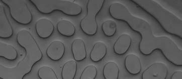
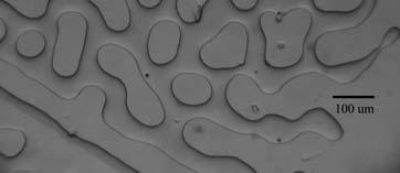
20
21 Grand Challenges of Soft Patterning Top-down Meets Self-Organization!! Sub-micron Features on Large areas (> cm; beyond!) Rapid (m per second!! ); (roll-to-roll?; parallel) Integration across Different Materials (hydrogels, ceramics, carbon ) Process Complexity; Resources, Cost. Patterning beyond Master: One Master, Many Slaves In-situ Tuning of Patterns Programmable Patterning


22 Functional Nano-structured Interfaces: Smart-adhesives

 Setae of Gecko Adhesive pads of")

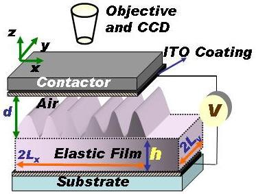
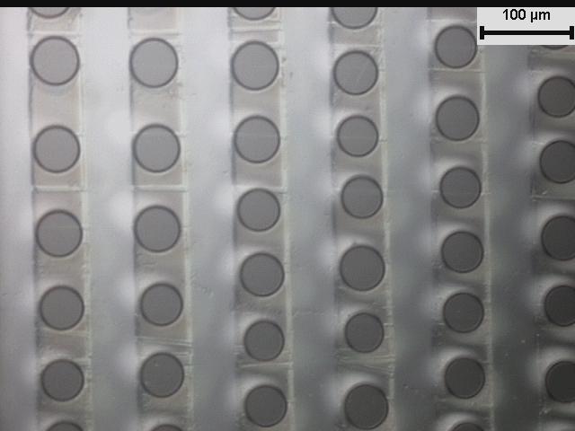
23 Producing High Strength Re-usable Soft Adhesives: Bio-inspired Adhesion Examples of Bioadhesives (Majumder, Ghatak & Sharma; Science, 2007) Setae of Gecko Adhesive pads of insects F G, Elastic Film t d h 0.9 J/m Microfluidic adhesive

24 Fabricating in Exotic Functional Materials: Carbon: Micro/nano Webs and C-MEMS Energy: micro battery, micro-fuel cell, super capacitor. Electronics: molecular switches, memory Biomaterials: C-MEMS. Environment: Adsorption & catalytic media With Marc Madou, UCI


25 Difficult to Fabricate Functional Materials: Carbon Energy: micro-fuel cell, micro battery, super capacitor.; Biomaterials. Functionalization: Collaborator: Marc Madou, UCI Carbon fibres Pyrolyzed Polymer structures!! Stability : Stick
26 Nano-Imprinting Challenges: Uniform high pressure/temperature Conformal contact/curved surfaces Stamp Removal Meeting the Challenges Flexible thin foil stamps Solvent vapor assisted softening of polymer films Spontaneous conformal contact by adhesive forces Soluble moulds/masters/stamps


27 Almost any polymer on any surface!! Sharma et al., Macromolecules 2006 Structural Colors by Micro-patterning: Adhesive Force Lithography with Flexible Foils: Variety of Surfaces and Materials PS polymer; 6 cm 2 Curved Hydrogel

28 Patterning Beyond Master : Pattern Miniaturization Sharma et al. 400 nm structures starting from 800 nm master

29 Patterning by Elastic Contact Instability: A New Micro/Nano Fabrication Tool pattern length scale ~ 3 H A. Positive Replica B. 2-D Bifurcation C. Compress: Negative replica D. Pull E. Feature size reduction: Thin film Sharma et al. Langmuir 2006 W ~ 2L

30 Patterning by Electric Fields: A New Fabrication Tool Sharma, Shenoy, Narayan et al., Adv Mat 2006


31 Controlled Self-organized Dewetting: A New Fabrication Tool Sharma et al.
 im print m aterial substrate im print (force,uv, heat) release ISSUES: RIE etch A.")
32 Robust Nanoimprint Lithography 1. Imprinting of soft elastic films Sharma & Soles (NIST) 2. Imprinting of viscous polymeric liquid films m old (Si, Q uartz) im print m aterial substrate im print (force,uv, heat) release ISSUES: RIE etch A. Stress, strain, flow and structure relationships B. Stability and fidelity of imprinted structures C. Metrology


33 Nano-Patterning of Surfaces by Self-assembly: Sandeep Verma Adenine- Silver Metallaquartet a b HOPG J. Am. Chem. Soc. 2006, 128, Adenine- Silver Duplex HOPG a b J. Am. Chem. Soc. 2007, 129,


34 Sandeep Verma, Chemistry a b a b J. Am. Chem. Soc. 2006, 128, J. Am. Chem. Soc. 2007, 129,


35 Peptide morphologies FFPP PPFF PFFP J. Pep. Sci. 2007, 14, Chem. Eur. J. 2008, 14, Angew. Chem. 2008, 47, Angew. Chem. 2008, 47,

 Ag colloid in aqueous SDS (R. Budhani et al.")
36 Laser Ablation Assisted Growth of Quantum Dots & Quantum Wires and Their Magnetic Properties 50 nm (a) Counts (b) (b) Diameter (nm) Ag colloid in aqueous SDS (R. Budhani et al.)
 (b) (c) M (emu/cc) -600 600 M (emu/cc) -600 600 M (emu/cc) 600 0 0 0-60 -30 0 30 60 (d) (e) (f) T G")

.")
37 T G = C 2.0 μm T G = C 2.0 μm T G = C 2.0 μm (a) (b) (c) M (emu/cc) M (emu/cc) M (emu/cc) (d) (e) (f) T G = C T G = C Perpendicular In-plane Applied field (koe) CoPt Fractals and Nano dots Budhani, Rakshit et al. Appl. Phys. Lett (2006) SEM images and Perpendicular magnetization loops of 50 nm CoPt thin films deposited at various substrate temperatures at a growth rate of 0.4 Å/sec on single crystal STO (001). All the samples were post annealed for 25 minutes. Magnetization panel for the sample grown C also shows data for in-plane configuration.
38 Fabrication using FIB 1. 2-D Patterning (masks, molds, stamps) 2. 3-D Structures (AFM tips, cantilevers, devices)


39 Focused Ion Beam: Nanomachining and Beyond Nova NanoLab NOVA NANO ANOLAB AB Nano- Milling Deposition Ion Beam (Ga KeV) Spot size 7 nm Scan Generator for SEM Scan Genera tor for FIB Sample (mounted on a precision SE D/ SI D Monit or


40 EXAMPLES Micro Squid with Nb Films; Anjan Gupta et al. Holes (100 nm dia.) drilled in NbSe2 for patterning the magnetic vortex states; Satyajit Banerjee et al. Platinum electrodes separation 50 nm; I-V characteristics; Child Langmuir law at nanometer scales; S. Bhattacharjee


41 Superconducting Nano-Devices 4 V-I CHARACTERISTIC of Nb JJ (180(L) x 170(w) x 80(t) nm 3 ) 4 V-I Characteristic of Nb SQUID (H=0) 2 2 voltage in mv dv/di in ohm I C ~ 80 µa PLOT of dv/di vs I Current in ma Current in ma Voltage in mv dv/di in ohm Current in ma Current in ma SQUID Loop Area: (3.3 x 3.3) μm 2 JJs:: 200(L) x 180(w) nm 2 Maskless optical lithography + FIB milling; A. Gupta et al.


42 Carbon Cantilevers and Particles on AFM Tip AFM measurements of force-distance require dense spherical carbon particles 2-5 micron attached to the AFM tip Kulkarni et al. Sharma et al.
![AFM Tips for Nanoindentation AFM tip of well defined shapes are required; grown Tungsten tips of hemispherical shape with the required end radius of 50 nm s [piezo displacement, nm] 160 140 120 100](/docs-images/80/82482251/images/43-0.jpg "80 60 40 20 (z 2,s 2 ) (z 1,s 1 ) range of analysis z =(z 1 -z 2 ) s = (s 2 -s 1 ) h = (z-s) tip movement Elastic modulus [MPa] 400 350 300 250 200 150 100 0 50-20 50 100 150 200 250 300 350 400 450")
43 AFM Tips for Nanoindentation AFM tip of well defined shapes are required; grown Tungsten tips of hemispherical shape with the required end radius of 50 nm s [piezo displacement, nm] (z 2,s 2 ) (z 1,s 1 ) range of analysis z =(z 1 -z 2 ) s = (s 2 -s 1 ) h = (z-s) tip movement Elastic modulus [MPa] z [diflection, nm] Fig 2. Vertical displacement h [indentation depth, nm] Fig. 3 Modulus vs indentation depth Sharma, Kar, Deva et al.


44 Meso-patterning of thin polymer films by atomic force microscope assisted electrohydrodynamic nanolithography 0 th 1 st 2 nd Xie, Chung, Bandyopadhyay, Sharma, et al, J. Applied Phys. 103, (2008). selected paper in Virtual Journal of Nanoscale Science &


45 Fabrication of Small Things: Ghatak, Sharma et al. Adv Mat (2007) Top-Down Bottom-up Self-organization Miniaturization
46 Over 70 publications in International Journals 3 patents filed and 1 disclosure 14 PhD students and several project staff trained In addition to the Unit funding ~ 15 Carores, 6 additional nano related projects ~ 7 carores generated Collaborations with Cambridge, NIST, Lehigh, UIC, JNCASR, Saha Institute, TRDDC, NUS.. Exciting new discoveries!!!!


47 Best way to predict the future is to invent it.
NPTEL. Instability and Patterning of Thin Polymer Films - Video course. Chemical Engineering.
 NPTEL Syllabus Instability and Patterning of Thin Polymer Films - Video course COURSE OUTLINE T h i s course will expose students to the science of sub-micron, meso and nanoscale patterning of surfaces
Nova 600 NanoLab Dual beam Focused Ion Beam IITKanpur
 Nova 600 NanoLab Dual beam Focused Ion Beam system @ IITKanpur Dual Beam Nova 600 Nano Lab From FEI company (Dual Beam = SEM + FIB) SEM: The Electron Beam for SEM Field Emission Electron Gun Energy : 500
There's Plenty of Room at the Bottom
 There's Plenty of Room at the Bottom 12/29/1959 Feynman asked why not put the entire Encyclopedia Britannica (24 volumes) on a pin head (requires atomic scale recording). He proposed to use electron microscope
Nanotechnology Fabrication Methods.
 Nanotechnology Fabrication Methods. 10 / 05 / 2016 1 Summary: 1.Introduction to Nanotechnology:...3 2.Nanotechnology Fabrication Methods:...5 2.1.Top-down Methods:...7 2.2.Bottom-up Methods:...16 3.Conclusions:...19
Superhydrophobic Surfaces
 Superhydrophobic Surfaces Glen McHale and Mike Newton School of Biomedical & Natural Sciences Nottingham Trent University, UK Email: glen.mchale@ntu.ac.uk The Laboratory Themes & Expertise Wetting of surfaces
Nano Materials and Devices
 Nano Materials and Devices Professor Michael Austin Platform Technologies Research Institute Nano Materials and Devices Program Aim: to develop an integrated capability in nanotechnology Design and modelling
Title Single Row Nano-Tribological Printing: A novel additive manufacturing method for nanostructures
 Nano-Tribological Printing: A novel additive manufacturing method for nanostructures H.S. Khare, N.N. Gosvami, I. Lahouij, R.W. Carpick 1 Mechanical Engineering and Applied Mechanics, University of Pennsylvania,
Title Single Row Nano-Tribological Printing: A novel additive manufacturing method for nanostructures
 Nano-Tribological Printing: A novel additive manufacturing method for nanostructures H.S. Khare, N.N. Gosvami, I. Lahouij, R.W. Carpick hkhare@seas.upenn.edu carpick@seas.upenn.edu carpick.seas.upenn.edu
Techniken der Oberflächenphysik (Techniques of Surface Physics)
") Techniken der Oberflächenphysik (Techniques of Surface Physics) Prof. Yong Lei & Dr. Yang Xu (& Liying Liang) Fachgebiet 3D-Nanostrukturierung, Institut für Physik Contact: yong.lei@tu-ilmenau.de; yang.xu@tu-ilmenau.de;
Techniken der Oberflächenphysik (Techniques of Surface Physics) Prof. Yong Lei & Dr. Yang Xu (& Liying Liang) Fachgebiet 3D-Nanostrukturierung, Institut für Physik Contact: yong.lei@tu-ilmenau.de; yang.xu@tu-ilmenau.de;
Research Activities Centre for Nanotechnology Indian Institute of Technology Guwahati
 Research Activities Centre for Nanotechnology Indian Institute of Technology Guwahati BROADER OBJECTIVES BROADER OBJECTIVES BROADER OBJECTIVES OF THE CENTRE FOR NANOTECHNOLOGY: To provide a state-of-the-art
Nanostructures Fabrication Methods
 Nanostructures Fabrication Methods bottom-up methods ( atom by atom ) In the bottom-up approach, atoms, molecules and even nanoparticles themselves can be used as the building blocks for the creation of
Deposition of Multilayer Fibers and Beads by Near-Field Electrospinning for Texturing and 3D Printing Applications
 Deposition of Multilayer Fibers and Beads by Near-Field Electrospinning for Texturing and 3D Printing Applications Nicolas Martinez-Prieto, Jian Cao, and Kornel Ehmann Northwestern University SmartManufacturingSeries.com
Scanning Probe Microscopy. Amanda MacMillan, Emmy Gebremichael, & John Shamblin Chem 243: Instrumental Analysis Dr. Robert Corn March 10, 2010
 Scanning Probe Microscopy Amanda MacMillan, Emmy Gebremichael, & John Shamblin Chem 243: Instrumental Analysis Dr. Robert Corn March 10, 2010 Scanning Probe Microscopy High-Resolution Surface Analysis
ESH Benign Processes for he Integration of Quantum Dots (QDs)
") ESH Benign Processes for he Integration of Quantum Dots (QDs) PIs: Karen K. Gleason, Department of Chemical Engineering, MIT Graduate Students: Chia-Hua Lee: PhD Candidate, Department of Material Science
ESH Benign Processes for he Integration of Quantum Dots (QDs) PIs: Karen K. Gleason, Department of Chemical Engineering, MIT Graduate Students: Chia-Hua Lee: PhD Candidate, Department of Material Science
Nanomechanics Measurements and Standards at NIST
 Nanomechanics Measurements and Standards at NIST Robert F. Cook Deputy Chief, Ceramics Division Leader, Nanomechanical Properties Group robert.cook@nist.gov NIST Mission Promote U.S. innovation and industrial
Integrating MEMS Electro-Static Driven Micro-Probe and Laser Doppler Vibrometer for Non-Contact Vibration Mode SPM System Design
 Tamkang Journal of Science and Engineering, Vol. 12, No. 4, pp. 399 407 (2009) 399 Integrating MEMS Electro-Static Driven Micro-Probe and Laser Doppler Vibrometer for Non-Contact Vibration Mode SPM System
Fabrication at the nanoscale for nanophotonics
 Fabrication at the nanoscale for nanophotonics Ilya Sychugov, KTH Materials Physics, Kista silicon nanocrystal by electron beam induced deposition lithography Outline of basic nanofabrication methods Devices
Fabrication of ordered array at a nanoscopic level: context
 Fabrication of ordered array at a nanoscopic level: context Top-down method Bottom-up method Classical lithography techniques Fast processes Size limitations it ti E-beam techniques Small sizes Slow processes
Imaging Polymer Morphology Using Atomic Force Microscopy
 Imaging Polymer Morphology Using Atomic Force Microscopy Russell J. Composto Materials Science and Engineering, and the Laboratory for Research on the Structure of Matter, University of Pennsylvania Agilent
Nanomaterials and their Optical Applications
 Nanomaterials and their Optical Applications Winter Semester 2013 Lecture 02 rachel.grange@uni-jena.de http://www.iap.uni-jena.de/multiphoton Lecture 2: outline 2 Introduction to Nanophotonics Theoretical
NANO SCIENCE AND TECHNOLOGY THE INDIAN SCENE
 NANO SCIENCE AND TECHNOLOGY THE INDIAN SCENE DR. PRAVEER ASTHANA MINISTRY OF SCIENCE AND TECHNOLOGY (DEPARTMENT OF SCIENCE AND TECHNOLOGY) GOVERNMENT OF INDIA WHAT HAVE WE DONE SO FAR? Basic Research in
Institute for Electron Microscopy and Nanoanalysis Graz Centre for Electron Microscopy
 Institute for Electron Microscopy and Nanoanalysis Graz Centre for Electron Microscopy Micromechanics Ass.Prof. Priv.-Doz. DI Dr. Harald Plank a,b a Institute of Electron Microscopy and Nanoanalysis, Graz
Research to Improve Photovoltaic (PV) Cell Efficiency by Hybrid Combination of PV and Thermoelectric Cell Elements.
 Cell Efficiency by Hybrid Combination of PV and Thermoelectric Cell Elements.") UNIVERSITY OF CENTRAL FLORIDA Research to Improve Photovoltaic (PV) Cell Efficiency by Hybrid Combination of PV and Thermoelectric Cell Elements. Page 129 PI: Nicoleta Sorloaica-Hickman, Robert Reedy Students:
UNIVERSITY OF CENTRAL FLORIDA Research to Improve Photovoltaic (PV) Cell Efficiency by Hybrid Combination of PV and Thermoelectric Cell Elements. Page 129 PI: Nicoleta Sorloaica-Hickman, Robert Reedy Students:
Positioning, Structuring and Controlling with Nanoprecision
 Positioning, Structuring and Controlling with Nanoprecision Regine Hedderich 1,2, Tobias Heiler 2,3, Roland Gröger 2,3, Thomas Schimmel 2,3 and Stefan Walheim 2,3 1 Network NanoMat 2 Institute of Nanotechnology,
Technologies VII. Alternative Lithographic PROCEEDINGS OF SPIE. Douglas J. Resnick Christopher Bencher. Sponsored by. Cosponsored by.
 PROCEEDINGS OF SPIE Alternative Lithographic Technologies VII Douglas J. Resnick Christopher Bencher Editors 23-26 February 2015 San Jose, California, United States Sponsored by SPIE Cosponsored by DNS
Contents. Foreword by Darrell H. Reneker
 Table of Foreword by Darrell H. Reneker Preface page xi xiii 1 Introduction 1 1.1 How big is a nanometer? 1 1.2 What is nanotechnology? 1 1.3 Historical development of nanotechnology 2 1.4 Classification
Electrochemically Synthesized Multi-block
 Electrochemically Synthesized Multi-block Nanorods Sungho Park SungKyunKwan University, Department of Chemistry & SKKU Advanced Institute of Nanotechnology (SAINT) J. Am. Chem. Soc. 2003, 125, 2282-2290
Printing Silver Nanogrids on Glass: A Hands-on Investigation of Transparent Conductive Electrodes
 Printing Silver Nanogrids on Glass: A Hands-on Investigation of Transparent Conductive Electrodes Silver Nanogrid/Nanowire Importance The next generation of optoelectronic devices requires transparent
SELF-ASSEMBLY AND NANOTECHNOLOGY A Force Balance Approach
 SELF-ASSEMBLY AND NANOTECHNOLOGY A Force Balance Approach Yoon S. Lee Scientific Information Analyst Chemical Abstracts Service A Division of the American Chemical Society Columbus, Ohio WILEY A JOHN WILEY
A Novel Self-aligned and Maskless Process for Formation of Highly Uniform Arrays of Nanoholes and Nanopillars
 Nanoscale Res Lett (2008) 3: 127 DOI 10.1007/s11671-008-9124-6 NANO EXPRESS A Novel Self-aligned and Maskless Process for Formation of Highly Uniform Arrays of Nanoholes and Nanopillars Wei Wu Æ Dibyendu
Positioning, Structuring and Controlling with Nanoprecision
 Positioning, Structuring and Controlling with Nanoprecision Regine Hedderich 1,2, Tobias Heiler 2,3, Roland Gröger 2,3, Thomas Schimmel 2,3, and Stefan Walheim 2,3 1 Network NanoMat 2 Institute of Nanotechnology,
29: Nanotechnology. What is Nanotechnology? Properties Control and Understanding. Nanomaterials
 29: Nanotechnology What is Nanotechnology? Properties Control and Understanding Nanomaterials Making nanomaterials Seeing at the nanoscale Quantum Dots Carbon Nanotubes Biology at the Nanoscale Some Applications
Characterization of MEMS Devices
 MEMS: Characterization Characterization of MEMS Devices Prasanna S. Gandhi Assistant Professor, Department of Mechanical Engineering, Indian Institute of Technology, Bombay, Recap Characterization of MEMS
2D Materials Research Activities at the NEST lab in Pisa, Italy. Stefan Heun NEST, Istituto Nanoscienze-CNR and Scuola Normale Superiore, Pisa, Italy
 2D Materials Research Activities at the NEST lab in Pisa, Italy Stefan Heun NEST, Istituto Nanoscienze-CNR and Scuola Normale Superiore, Pisa, Italy 2D Materials Research Activities at the NEST lab in
Research Team name: Technology Research Center Laboratory, Selcuk University Presenter name: Prof. Dr. Mustafa Ersoz
 Research Team name: Technology Research Center Laboratory, Selcuk University Presenter name: Prof. Dr. Mustafa Ersoz Team Presentation Annual Workshop, COST Action MP1106 Dublin, September, 2012 Research
Chapter 10. Nanometrology. Oxford University Press All rights reserved.
 Chapter 10 Nanometrology Oxford University Press 2013. All rights reserved. 1 Introduction Nanometrology is the science of measurement at the nanoscale level. Figure illustrates where nanoscale stands
High-resolution Characterization of Organic Ultrathin Films Using Atomic Force Microscopy
 High-resolution Characterization of Organic Ultrathin Films Using Atomic Force Microscopy Jing-jiang Yu Nanotechnology Measurements Division Agilent Technologies, Inc. Atomic Force Microscopy High-Resolution
MEMS Metrology. Prof. Tianhong Cui ME 8254
 MEMS Metrology Prof. Tianhong Cui ME 8254 What is metrology? Metrology It is the science of weights and measures Refers primarily to the measurements of length, weight, time, etc. Mensuration- A branch
Chapter 1 Introduction
 Chapter 1 Introduction A nanometer (nm) is one billionth (10-9 ) of a meter. Nanoscience can be defined as the science of objects and phenomena occurring at the scale of 1 to 100 nm. The range of 1 100
Nanostrukturphysik (Nanostructure Physics)
") Nanostrukturphysik (Nanostructure Physics) Prof. Yong Lei & Dr. Yang Xu Fachgebiet 3D-Nanostrukturierung, Institut für Physik Contact: yong.lei@tu-ilmenau.de; yang.xu@tu-ilmenau.de Office: Unterpoerlitzer
Nanostrukturphysik (Nanostructure Physics) Prof. Yong Lei & Dr. Yang Xu Fachgebiet 3D-Nanostrukturierung, Institut für Physik Contact: yong.lei@tu-ilmenau.de; yang.xu@tu-ilmenau.de Office: Unterpoerlitzer
A. Optimizing the growth conditions of large-scale graphene films
 1 A. Optimizing the growth conditions of large-scale graphene films Figure S1. Optical microscope images of graphene films transferred on 300 nm SiO 2 /Si substrates. a, Images of the graphene films grown
NANOCOMPOSITE THIN FILMS:
 NANOCOMPOSITE THIN FILMS: Assembly, Characterizations, & Applications Chaoyang Jiang Department of Chemistry The University of South Dakota St. Louis, June 26, 2008 Forest Products &Nanocomposite P. Monteiro@UC
Instrumentation and Operation
 Instrumentation and Operation 1 STM Instrumentation COMPONENTS sharp metal tip scanning system and control electronics feedback electronics (keeps tunneling current constant) image processing system data
And Manipulation by Scanning Probe Microscope
 Basic 15 Nanometer Scale Measurement And Manipulation by Scanning Probe Microscope Prof. K. Fukuzawa Dept. of Micro/Nano Systems Engineering Nagoya University I. Basics of scanning probe microscope Basic
Nanoscale Issues in Materials & Manufacturing
 Nanoscale Issues in Materials & Manufacturing ENGR 213 Principles of Materials Engineering Module 2: Introduction to Nanoscale Issues Top-down and Bottom-up Approaches for Fabrication Winfried Teizer,
Diamond-like-carbon (DLC) master creation for use in soft lithography using the Atomic Force Microscope (AFM)
 master creation for use in soft lithography using the Atomic Force Microscope (AFM)") Diamond-like-carbon (DLC) master creation for use in soft lithography using the Atomic Force Microscope (AFM) Author Watson, Gregory, Myhra, S., Watson, Jolanta Published 2007 Journal Title Journal of
Diamond-like-carbon (DLC) master creation for use in soft lithography using the Atomic Force Microscope (AFM) Author Watson, Gregory, Myhra, S., Watson, Jolanta Published 2007 Journal Title Journal of
Micro/nano and precision manufacturing technologies and applications
 The 4th China-American Frontiers of Engineering Symposium Micro/nano and precision manufacturing technologies and applications Dazhi Wang School of Mechanical Engineering Dalian University of Technology
Lab to Market. T.A. Abinandanan Indian Institute of Science Bengaluru
 Lab to Market T.A. Abinandanan Indian Institute of Science Bengaluru Simputer (2002) from IISc pioneered the concept of research-based start-ups NanoSniff from IIT-B PathShodh (IISc) NHHID (Anna University)
Nanostructure. Materials Growth Characterization Fabrication. More see Waser, chapter 2
 Nanostructure Materials Growth Characterization Fabrication More see Waser, chapter 2 Materials growth - deposition deposition gas solid Physical Vapor Deposition Chemical Vapor Deposition Physical Vapor
Please allow us to demonstrate our capabilities and test us testing your samples!
 We determine properties of surfaces, thin films, and layer structures Hardness Young s modulus Scratch, friction, and wear tests Topography Mapping of thermal, magnetic, and electronic properties Please
Revealing High Fidelity of Nanomolding Process by Extracting the Information from AFM Image with Systematic Artifacts
 Revealing High Fidelity of Nanomolding Process by Extracting the Information from AFM Image with Systematic Artifacts Sajal Biring* Department of Electronics Engineering and Organic Electronics Research
Dip-Pen Lithography 1
 Dip-Pen Lithography 1 A Brief History of Writing Instruments From Quills and Bamboos to fountain pens and brushes M. Klein and Henry W. Wynne received US patent #68445 in 1867 for an ink chamber and delivery
Seminars in Nanosystems - I
 Seminars in Nanosystems - I Winter Semester 2011/2012 Dr. Emanuela Margapoti Emanuela.Margapoti@wsi.tum.de Dr. Gregor Koblmüller Gregor.Koblmueller@wsi.tum.de Seminar Room at ZNN 1 floor Topics of the
Supporting Information. Fast Synthesis of High-Performance Graphene by Rapid Thermal Chemical Vapor Deposition
 1 Supporting Information Fast Synthesis of High-Performance Graphene by Rapid Thermal Chemical Vapor Deposition Jaechul Ryu, 1,2, Youngsoo Kim, 4, Dongkwan Won, 1 Nayoung Kim, 1 Jin Sung Park, 1 Eun-Kyu
General concept and defining characteristics of AFM. Dina Kudasheva Advisor: Prof. Mary K. Cowman
 General concept and defining characteristics of AFM Dina Kudasheva Advisor: Prof. Mary K. Cowman Overview Introduction History of the SPM invention Technical Capabilities Principles of operation Examples
Appendix A. Assessments Points 4 Mode of Assessments. New Course Code and Title Course Coordinator. MS741M Nanomaterials
 New Course Code and Title Course Coordinator Details of Course MS741M Nanomaterials AP Jason Xu (Course Coordinator) AP Xue Can Rationale for introducing this course This course will cover the subject
Dr. Aoife Morrin. School of Chemical Sciences Dublin City University Ireland. The National Centre for Sensor Research
 INVESTIGATION OF NANOSTRUCTURED MATERIALS FOR NOVEL BIOSENSOR FABRICATION METHODOLOGIES Dr. Aoife Morrin National Centre for Sensor Research School of Chemical Sciences Dublin City University Ireland Introduction
In the name of Allah
 In the name of Allah Nano chemistry- 4 th stage Lecture No. 1 History of nanotechnology 16-10-2016 Assistance prof. Dr. Luma Majeed Ahmed lumamajeed2013@gmail.com, luma.ahmed@uokerbala.edu.iq Nano chemistry-4
Bringing optics into the nanoscale a double-scanner AFM brings advanced optical experiments within reach
 Bringing optics into the nanoscale a double-scanner AFM brings advanced optical experiments within reach Beyond the diffraction limit The resolution of optical microscopy is generally limited by the diffraction
Chapter 12. Nanometrology. Oxford University Press All rights reserved.
 Chapter 12 Nanometrology Introduction Nanometrology is the science of measurement at the nanoscale level. Figure illustrates where nanoscale stands in relation to a meter and sub divisions of meter. Nanometrology
Overview of the main nano-lithography techniques
 Overview of the main nano-lithography techniques Soraya Sangiao sangiao@unizar.es Outline Introduction: Nanotechnology. Nano-lithography techniques: Masked lithography techniques: Photolithography. X-ray
Graphene Fundamentals and Emergent Applications
 Graphene Fundamentals and Emergent Applications Jamie H. Warner Department of Materials University of Oxford Oxford, UK Franziska Schaffel Department of Materials University of Oxford Oxford, UK Alicja
Flexible nonvolatile polymer memory array on
 Supporting Information for Flexible nonvolatile polymer memory array on plastic substrate via initiated chemical vapor deposition Byung Chul Jang, #a Hyejeong Seong, #b Sung Kyu Kim, c Jong Yun Kim, a
Course file PPY15204 Nanoscience and Nanomaterials Table of Contents
 Department Physics Nanotechnology : M.sc Physics Course file PPY15204 Table Contents Second Year MSc Physics (2015-2016 Regulation) Detailed Lesson Plan UNIT-I: INTRODUCTION TO NANOTECHNOLOGY History Importance
26.542: COLLOIDAL NANOSCIENCE & NANOSCALE ENGINEERING Fall 2013
 26.542: COLLOIDAL NANOSCIENCE & NANOSCALE ENGINEERING Fall 2013 Classes: Thurs, 6-9 pm; Ball Hall Room 208 Professor: Dr. B. Budhlall Office: Ball Hall 203B, Phone: 978-934-3414 Email: Bridgette_Budhlall@uml.edu
Image courtesy of Dr James Bendall, University of Cambridge, UK. Discover the secrets h of the Nanoworld
 Image courtesy of Dr James Bendall, University of Cambridge, UK. Discover the secrets h of the Nanoworld Nano has become a buzz word in popular culture to just mean small. To understand nanotechnology
Self-assembled nanostructures for antireflection optical coatings
 Self-assembled nanostructures for antireflection optical coatings Yang Zhao 1, Guangzhao Mao 2, and Jinsong Wang 1 1. Deaprtment of Electrical and Computer Engineering 2. Departmentof Chemical Engineering
Mechanical Characterization of High Aspect Ratio Silicon Nanolines
 Mater. Res. Soc. Symp. Proc. Vol. 1086 2008 Materials Research Society 1086-U05-07 Mechanical Characterization of High Aspect Ratio Silicon Nanolines Bin Li 1, Huai Huang 1, Qiu Zhao 1, Zhiquan Luo 1,
A New Dielectrophoretic Coating Process for Depositing Thin Uniform Coatings on Films and Fibrous Surfaces
 A New Dielectrophoretic Coating Process for Depositing Thin Uniform Coatings on Films and Fibrous Surfaces by Angelo Yializis Ph.D., Xin Dai Ph.D. Sigma Technologies International Tucson, AZ USA SIGMA
Crystalline Surfaces for Laser Metrology
 Crystalline Surfaces for Laser Metrology A.V. Latyshev, Institute of Semiconductor Physics SB RAS, Novosibirsk, Russia Abstract: The number of methodological recommendations has been pronounced to describe
Supporting Information
 Supporting Information Superstructural Raman Nanosensors with Integrated Dual Functions for Ultrasensitive Detection and Tunable Release of Molecules Jing Liu #, Jianhe Guo #, Guowen Meng and Donglei Fan*
Nanotechnology. Gavin Lawes Department of Physics and Astronomy
 Nanotechnology Gavin Lawes Department of Physics and Astronomy Earth-Moon distance 4x10 8 m (courtesy NASA) Length scales (Part I) Person 2m Magnetic nanoparticle 5x10⁻⁹ m 10 10 m 10 5 m 1 m 10-5 m 10-10
Imaging Methods: Scanning Force Microscopy (SFM / AFM)
") Imaging Methods: Scanning Force Microscopy (SFM / AFM) The atomic force microscope (AFM) probes the surface of a sample with a sharp tip, a couple of microns long and often less than 100 Å in diameter.
Imaging Methods: Scanning Force Microscopy (SFM / AFM) The atomic force microscope (AFM) probes the surface of a sample with a sharp tip, a couple of microns long and often less than 100 Å in diameter.
Physics and Chemistry of Interfaces
 Hans Jürgen Butt, Karlheinz Graf, and Michael Kappl Physics and Chemistry of Interfaces Second, Revised and Enlarged Edition WILEY- VCH WILEY-VCH Verlag GmbH & Co. KGaA Contents Preface XI 1 Introduction
Nanostrukturphysik (Nanostructure Physics)
") Nanostrukturphysik (Nanostructure Physics) Prof. Yong Lei & Dr. Yang Xu Fachgebiet 3D-Nanostrukturierung, Institut für Physik Contact: yong.lei@tu-ilmenau.de; yang.xu@tu-ilmenau.de Office: Unterpoerlitzer
Nanostrukturphysik (Nanostructure Physics) Prof. Yong Lei & Dr. Yang Xu Fachgebiet 3D-Nanostrukturierung, Institut für Physik Contact: yong.lei@tu-ilmenau.de; yang.xu@tu-ilmenau.de Office: Unterpoerlitzer
JOHN G. EKERDT RESEARCH FOCUS
 JOHN G. EKERDT RESEARCH FOCUS We study the surface, growth and materials chemistry of metal, dielectric, ferroelectric, and polymer thin films. We seek to understand and describe nucleation and growth
Current and Emergent Developments
 Self Assembly and Biologically Inspired Processes in Applied Nanotechnology: Current and Emergent Developments Charles Ostman VP, Electronics & Photonics Forum chair NanoSig Senior Consultant Silicon Valley
Contents. Preface...xv List of Contributors...xvii
 Preface...xv List of Contributors...xvii CHAPTER 1 Nanotechnology to Nanomanufacturing... 1 1.1 Introduction...1 1.2 Approaches to Nanotechnology...2 1.3 Transition from Nanotechnology to Nanomanufacturing...3
Fabrication and Domain Imaging of Iron Magnetic Nanowire Arrays
 Abstract #: 983 Program # MI+NS+TuA9 Fabrication and Domain Imaging of Iron Magnetic Nanowire Arrays D. A. Tulchinsky, M. H. Kelley, J. J. McClelland, R. Gupta, R. J. Celotta National Institute of Standards
Supplementary Figure 1 Detailed illustration on the fabrication process of templatestripped
 Supplementary Figure 1 Detailed illustration on the fabrication process of templatestripped gold substrate. (a) Spin coating of hydrogen silsesquioxane (HSQ) resist onto the silicon substrate with a thickness
MSN551 LITHOGRAPHY II
 MSN551 Introduction to Micro and Nano Fabrication LITHOGRAPHY II E-Beam, Focused Ion Beam and Soft Lithography Why need electron beam lithography? Smaller features are required By electronics industry:
Title of file for HTML: Supplementary Information Description: Supplementary Figures and Supplementary References
 Title of file for HTML: Supplementary Information Description: Supplementary Figures and Supplementary References Supplementary Figure 1. SEM images of perovskite single-crystal patterned thin film with
From nanophysics research labs to cell phones. Dr. András Halbritter Department of Physics associate professor
 From nanophysics research labs to cell phones Dr. András Halbritter Department of Physics associate professor Curriculum Vitae Birth: 1976. High-school graduation: 1994. Master degree: 1999. PhD: 2003.
Subject Index. See https://pubs.acs.org/sharingguidelines for options on how to legitimately share published articles.
 Subject Index Downloaded via 148.251.232.83 on July 22, 2018 at 01:11:58 (UTC). See https://pubs.acs.org/sharingguidelines for options on how to legitimately share published articles. A American Chemical
Nanotechnology Nanofabrication of Functional Materials. Marin Alexe Max Planck Institute of Microstructure Physics, Halle - Germany
 Nanotechnology Nanofabrication of Functional Materials Marin Alexe Max Planck Institute of Microstructure Physics, Halle - Germany Contents Part I History and background to nanotechnology Nanoworld Nanoelectronics
SEMATECH Knowledge Series 2010
 SEMATECH Knowledge Series 2010 Summary of the SEMATECH Workshop on Directed Self Assembly Lloyd Litt SEMATECH/GF Bill Hinsberg - IBM 20 October 2010 Kobe, Japan Copyright 2010 Advanced Materials Research
ALIGNMENT ACCURACY IN A MA/BA8 GEN3 USING SUBSTRATE CONFORMAL IMPRINT LITHOGRAPHY (SCIL)
") ALIGNMENT ACCURACY IN A MA/BA8 GEN3 USING SUBSTRATE CONFORMAL IMPRINT LITHOGRAPHY (SCIL) Robert Fader Fraunhofer Institute for Integrated Systems and Device Technology (IISB) Germany Ulrike Schömbs SUSS
ALIGNMENT ACCURACY IN A MA/BA8 GEN3 USING SUBSTRATE CONFORMAL IMPRINT LITHOGRAPHY (SCIL) Robert Fader Fraunhofer Institute for Integrated Systems and Device Technology (IISB) Germany Ulrike Schömbs SUSS
State of São Paulo. Brasil. Localization. Santo André
 Brasil State of São Paulo Localization Santo André The Group www.crespilho.com Frank N. Crespilho Pablo R. S. Abdias Group Leader Synthesis of nanostructured materials using polyelectrolytes Andressa R.
OPTI510R: Photonics. Khanh Kieu College of Optical Sciences, University of Arizona Meinel building R.626
 OPTI510R: Photonics Khanh Kieu College of Optical Sciences, University of Arizona kkieu@optics.arizona.edu Meinel building R.626 Announcements HW#3 is assigned due Feb. 20 st Mid-term exam Feb 27, 2PM
Keywords- Focused Ion Beams, Nanostructuring, Polymers, Functionalization, Electron Microscopy, Surface Modification
 THE USE OF FOCUSED ELECTRON AND ION BEAMS FOR THE FUNCTIONALIZATION AND NANOSTRUCTURING OF POLYMER SURFACES 1 MELTEM SEZEN, 2 FERAY BAKAN 1,2 SUNUM Sabanci University Turkey E-mail: 1 meltemsezen@sabanciuniv.edu,
EV Group. Engineered Substrates for future compound semiconductor devices
 EV Group Engineered Substrates for future compound semiconductor devices Engineered Substrates HB-LED: Engineered growth substrates GaN / GaP layer transfer Mobility enhancement solutions: III-Vs to silicon
Basic Laboratory. Materials Science and Engineering. Atomic Force Microscopy (AFM)
") Basic Laboratory Materials Science and Engineering Atomic Force Microscopy (AFM) M108 Stand: 20.10.2015 Aim: Presentation of an application of the AFM for studying surface morphology. Inhalt 1.Introduction...
Basic Laboratory Materials Science and Engineering Atomic Force Microscopy (AFM) M108 Stand: 20.10.2015 Aim: Presentation of an application of the AFM for studying surface morphology. Inhalt 1.Introduction...
Master Thesis Projects at NanoLab
 Master Thesis Projects at NanoLab Micro and Nanostructured Materials Lab - NanoLab Department of Energy (Cesnef site Building 19) Leonardo Campus NEMAS Center for NanoEngineered Materials and Surfaces
Metrology is not a cost factor, but a profit center
 Edition February 2018 Semiconductor technology & processing Metrology is not a cost factor, but a profit center In recent years, remarkable progress has been made in the field of metrology, which is crucial
Molecular Electronics For Fun and Profit(?)
") Molecular Electronics For Fun and Profit(?) Prof. Geoffrey Hutchison Department of Chemistry University of Pittsburgh geoffh@pitt.edu July 22, 2009 http://hutchison.chem.pitt.edu Moore s Law: Transistor
Molecular Electronics For Fun and Profit(?) Prof. Geoffrey Hutchison Department of Chemistry University of Pittsburgh geoffh@pitt.edu July 22, 2009 http://hutchison.chem.pitt.edu Moore s Law: Transistor
MICRO-SCALE SHEET RESISTANCE MEASUREMENTS ON ULTRA SHALLOW JUNCTIONS
 MICRO-SCALE SHEET RESISTANCE MEASUREMENTS ON ULTRA SHALLOW JUNCTIONS Christian L. Petersen, Rong Lin, Dirch H. Petersen, Peter F. Nielsen CAPRES A/S, Burnaby, BC, Canada CAPRES A/S, Lyngby, Denmark We
Solutions for Assignment-8
 Solutions for Assignment-8 Q1. The process of adding impurities to a pure semiconductor is called: [1] (a) Mixing (b) Doping (c) Diffusing (d) None of the above In semiconductor production, doping intentionally
Contents. What is AFM? History Basic principles and devices Operating modes Application areas Advantages and disadvantages
 Contents What is AFM? History Basic principles and devices Operating modes Application areas Advantages and disadvantages Figure1: 2004 Seth Copen Goldstein What is AFM? A type of Scanning Probe Microscopy
Reactive Inkjet Printing. Patrick J. Smith University of Sheffield
 Reactive Inkjet Printing Patrick J. Smith University of Sheffield 15 th November 2017 Sheffield Applied Inkjet Research Lab Here we are! Main Research themes Tissue engineering Reactive Inkjet Printing
Nanotechnology: Today and tomorrow
 Nanotechnology: Today and tomorrow Horst-Günter Rubahn NanoSYD Mads Clausen Instituttet Syddansk Universitet Alsion 2 6400 Sønderborg Agenda Alsion A bit about nano Nanoproducts Top down vs. bottom up