Visit
|
|
|
- Melissa Quinn
- 5 years ago
- Views:
Transcription

1 FUNCTIONALIZATION AND APPLICATION OF NANOMATERIALS FOR ELECTRONIC APPLICATIONS Dr Toby Sainsbury Materials Division National Physical Laboratory, London, United Kingdom Your Delegate Webinar Control Panel Open and close your panel Full screen view Raise hand for Q&A at the end Submit text questions during or at the end NPL Management Ltd -Commercial 2
2 NPL EI Free Technology Webinars Environmental Robustness: Performance Coatings & High Temperature Interconnects Tuesday 3 September NPL Cleaning & Contamination Testing Causes & Cures Webinar Tuesday 22nd October Other Group Activity NPL Cleaning & Contamination Testing Center at Productronica th November Productronica, Germany Conformal Coating Application & Testing Center - NEW Electronics Birmingham th April 2014 NEC Birmingham Productronica, Germany NPL Cleaning & Contamination Testing Center th November Images show NPL Cleaning & Contamination Testing Center at IPC APEX 2013


3 Cleaning & Contamination Testing Center A FUNCTIONALIZATION AND APPLICATION OF NANOMATERIALS FOR ELECTRONIC APPLICATIONS Dr Toby Sainsbury Materials Division National Physical Laboratory, London, United Kingdom

4 OUTLINE NANOTECHNOLOGY PROPERTIES OF NANOMATERIALS 2D NANOMATERIALS GRAPHENE HEXAGONAL BORON NITRIDE ALTERNATIVE 2D NANOSHEETS FUNCTIONALIZED NANOMATERIALS ELECTRONIC APPLICATIONS OF FUNCTIONALIZED NANOMATERIALS CARBON NANOTUBE COMPOSITE SYSTEMS FUNCTIONALIZED 2D NANOSHEET SYSTEMS SUMMARY NANOTECHNOLOGY Nanotechnology: Technology involving benefits or attributes specifically assigned to the use or inclusion of materials which have one or more of their dimensions less than 100 nm. Synthesis of nanomaterials Application by assembly, processing, and integration of materials and structures Result: Stronger, more conductive, lighter, brighter, thermally conductive, smaller, faster, cheaper Bottom line. Financial, environmental, medical, societal, and scientific benefits resulting from nanotechnology NANOMATERIALS 1D NANOMATERIALS NANOTUBES: C, BN, WS 2, TiO 2 SnS 2, MoS 2, Wse NbS 2 NANOWIRES: Si, Ge, CdSe, ZnO, GaN, Au 3D NANOMATERIALS NANOPARTICLES Au, Ag, Cu, Pd, Pt, SiO 2, TiO 2, ZnO, NANORODS CdS, CdSe, PbSe, PbS, Au, Ag QUANTUM DOTS CdS, CdSe, CdTe, PbS, PbSe, PbTe DNA ASSEMBLIES TETRAPODS PEPTIDE FIBRES MX2 ONIONS MoS 2, WS 2 C 60 2D NANOMATERIALS GRAPHENE

 Non polar bonds ( = 0) Thermal conductivity (~5000 Wm 1 K 1 ) Planar structure (sp 2 ) Optical transmittance : 97.")
5 NANOMATERIALS PROPERTIES 1D NANOMATERIALS High aspect ratio Highly conductive Highly insulating Semi conductive Super conductive UV lasing Thermally conductive High strength 3D NANOMATERIALS Size tuneable plasmonic Conductive Semi conductive Insulating Fluorescent Catalytic Biocompatible Anti oxidative 2D NANOMATERIALS GRAPHENE PROPERTIES 2D NANOMATERIALS: GRAPHENE Conductive (mobility:200,000 cm 2 v 1 s 1 ) Chemically stability (<400 o C) Young's modulus: ~1 TPa Surface area: 2630 m 2 g 1 Low density (2.3 gcm 3 ) Non polar bonds ( = 0) Thermal conductivity (~5000 Wm 1 K 1 ) Planar structure (sp 2 ) Optical transmittance : 97.7% Crystalline ENVISAGED APPLICATIONS Thermal management metrology standards ( ) Composite materials Electronic (sub/super) Batteries/supercapacitors Sensing and Diagnostics Optoelectronics Catalysis CHALLENGES TO UTILIZATION: exfoliation, compatibilization, large area synthesis 10


6 Graphene: Theoretical surface area High intrinsic mobility High Youngs modulus Thermal conductivity Optical transmittance band gap Colour SYNTHESIS ADVANTAGES DRAWBACKS NEED RISK 2D NANOMATERIALS : GRAPHENE CVD, epitaxial SiC, exfoliation reasonably low cost, chemically stable yet highly amenable to specific chemistries. Abundant C as source material. Grain boundaries, defects, dislocations, intrinsic tendency to aggregate and stack. incompatible with large proportion of solvents, resins, condensed phase and molecular compounds. Zero band gap. Highly sensitive to environmental contaminants, substrate effects. Quality control assessment and metrology surrounding standard graphene reliable, scalable strategies for chemical integration strategies for production scale electronic integration with suitable substrates and electrodes. Drawbacks are pertinent and realistic reasons why graphene may not reach anywhere near the theoretical potential discussed at present. Highlights the need for metrology, manufacturing and processing research to be accelerated and for chemistries to be investigated. Alternative nanosheet materials require immediate attention. PROPERTIES 2D NANOMATERIALS : HEXAGONAL BORON NITRIDE Insulator (Eg ~5.5 ev) Chemically stability (0 850 o C) Mechanically robust (E 2d = 270 Nm 1 ) Large surface area Low density (2.3 gcm 3 ) Heteropolar bonds ( = 1) Thermal conductivity (0.3 W.cm 2. o C 1 ) Planar structure (sp 2 ) Macroscopic colour Crystalline ENVISAGED APPLICATIONS Thermal management Radiation Shielding Composite materials Electronic (sub/super) Storage/ Fuel Cell Sensing and Diagnostics Optoelectronics Catalysis CHALLENGES TO UTILIZATION: exfoliation, compatibilization, large area synthesis 12
 mobili es2 >60 cm2 V 1 s 1 (MoS2) on off current ra os up to 10 8 (MoS2) Thermoelectric (Bi2Te3) Topol ogical insulator (Bi2Te3) Range of mechanical properties Range of thermal properties")
7 2D NANOMATERIALS :ALTERNATIVE 2D NANOSHEETS RANGE OF MATERIAL PROPERTIES Band gap 0 6 ev, conductive to insulating Range of optical absorption wavelengths Luminescence quantum efficiency 1000 X bulk (MoS2) mobili es2 >60 cm2 V 1 s 1 (MoS2) on off current ra os up to 10 8 (MoS2) Thermoelectric (Bi2Te3) Topol ogical insulator (Bi2Te3) Range of mechanical properties Range of thermal properties APPLICATION OF 2D NANOMATERIALS catalysis Lubricant additives Nanoelectronics Sensors Nanocomposites Batteries Supercapacitors, Hydrogen storage Environmental science Metrology standards Themal management Barriers/membranes Dielectrics KEY FACTORS Synthesis, manipulation, integration Chemical functionalization FUNCTIONALIZED NANOMATERIALS
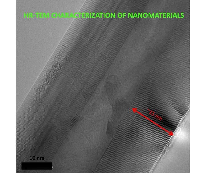
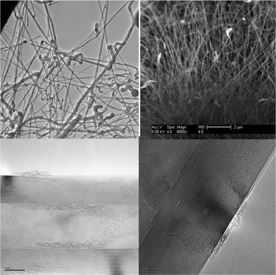
8 15 BNNT FUNCTIONALIZATION I TEM CHARACTERIZATION OF BNNTS 16

9 NANOTUBE FUNCTIONALIZATION NANOTUBE FUNCTIONALIZATION AMINE FUNCTIONALIZED BNNTS: BASE MATERIAL FOR EXTENSIVE LIBRARY OF FUNCTIONALIZED BNNTS 18


10 SELF ASSEMBLY: HYBRID SYSTEMS 19 SELF ASSEMBLY: HYBRID SYSTEMS BNNT-METAL SYSTEMS: Self-Assembly of Gold Nanoparticles at the Surface of Amine- and Thiol- Functionalized BNNTs 20
.")

11 SELF ASSEMBLY: HYBRID SYSTEMS Preparation of BNNT Pd nanoparticle Hybrid Structures Aqueous suspensions of thiol functionalized BNNTs and palladium nanoparticles are combined and allowed equilibrate (6h). Palladium nanoparticles are self assembled at the surface of BNNTs in solution. Interaction is mediated by the thiol Pd covalent bond formation. Typical Low resolution TEM images of DMAP-stabilized palladium nanoparticles self-assembled at the surface of different thiol-functionalized BNNTs. 21 ELECTRONIC APPLICATIONS OF FUNCTIONALIZED NANOTUBE SYSTEMS

 Silicon oxide is grown on a silicon wafer (2) Silicon nitride film is deposited by CVD (3) The silicon is then selectively back-etched with")
12 APPLICATION OF BNNT MATERIALS SENSING AND DIAGNOSTIC CdS QRs BNNTs 23 APPLICATION OF BNNT MATERIALS SENSING AND DIAGNOSTIC Electronic Transport properties of Au-NP/BNNT TEM compatible devices: Standard TEM architectures do not allow electron transmission. Silicon nitride (Si3N4) membranes have been used as electron transparent supports for TEM imaging. Schematic illustration of typical TEM compatible device structure. Fabrication process: (1) Silicon oxide is grown on a silicon wafer (2) Silicon nitride film is deposited by CVD (3) The silicon is then selectively back-etched with KOH (4) The oxide and nitride layers are exposed to HF to remove silicon oxide. 24
13 APPLICATION OF BNNT MATERIALS SENSING AND DIAGNOSTIC Current-Voltage characteristic of Gold Nanoparticle-functionalized BNNT structure (a) Current-voltage (I-V) property of gold nanoparticle-functionalized BNNT on the membrane device, which is measured at room temperature, and (b) a magnified I-V property of (a) and differential conductance plotted versus bias voltage. A series of current steps is observed. The charging energy and the energy between step levels are estimated to be 1 ev and 0.25 ev, respectively. The capacitance of the device is approximately 0.16 af. 25 APPLICATION OF BNNT MATERIALS SENSING AND DIAGNOSTIC Optical Response on the Transport Properties of Gold Nanoparticle Functionalized BNNTs 532 nm, <5mW Resistance ( ) 633 nm, =5mW Resistance ( ) 3.0x x x Frequency (Hz) 1.4x Conductance (S) Im[Z] ( ) Conductance (S) -3.0x R (M ) C (pf) Dark nm nm Nyquist plots: Optical Response of DPAP-Au-BNNT device Dark 532nm 633nm Frequency (Hz) Re[ Z] ( ) x
14 CARBON NANOTUBE COMPOSITE SYSTEMS CARBON NANOTUBE POLYMER COMPOSITES CNT Polymer composites Conductive Shielding materials Protective materials High strength composites Thermal management materials Properties highly dependent on nanotube type and dispersion.


15 ELECTRONIC CHARACTERIZATION OF CARBON NANOTUBE EPOXY COMPOSITES KEY ROLE OF DISPERSION NANOTUBE STRUCTURE POOR DISPERSION PERCOLATION HIGHLY CONDUCTIVE THERMAL CONDUCTION POOR MECHANICAL CONDUCTIVE POLYMER ESD MANAGEMENT ELECTRODE STRUCTURES NLO PROPERTIES ELECTRONIC CHARACTERIZATION OF CARBON NANOTUBE EPOXY COMPOSITES CHOICE OF NANOTUBE FIXED WEIGHT PERCENT: 1% SWNT MWNT DWNT F CNT I VARIABLE QUALITY WALL STRUCTURE DEFECTS LENGTH CHEMISTRY CLEAR DEMONSTRATION OF VARIABLE DISPERSION: VARIABLE CONDUCTIVITY COMPOSITES V
16 VARIABLE LOADING MWNT EPOXY COMPOSITES SINGLE VENDOR NANOTUBES ELECTRONIC CHARACTERIZATION OF CARBON NANOTUBE EPOXY COMPOSITES CHEMICAL FUNCTIONALIZATION OF CARBON NANOTUBES Manipulates surface energy of CNTs Introduces chemical functional groups Facilitates compatibility and specific chemical integration via bonding RESULTING DISPERSION DICTATES ELECTRICAL, THERMAL AND MECHANICAL PROPERTIESS
17 ELECTRONIC CHARACTERIZATION OF CARBON NANOTUBE EPOXY COMPOSITES HIGH QUALITY DIPSERSION ELECTRICAL ANALYSIS UNIFORM PROPERTIES CORRELATE WITH ALTERNATIVE CHARACTERIZATION ELECTRONIC CHARACTERIZATION OF CARBON NANOTUBE EPOXY COMPOSITES x10-9 MWCNT CT TCT 1% Epoxy Composite 0 to +/ 1000V EXCELLENT DISPERSION MECHANICALLY REINFORCING THERMALLY CONDUCTIVE HIGH TURN ON V DIELECTRIC PROPS BREAKDOWN PROTECTION ESD MANAGEMENT MATERIALS

18 ELECTRONIC CHARACTERIZATION OF CARBON NANOTUBE EPOXY COMPOSITES ESD AND LIGHTNING STRIKE MANAGEMENT Application of ESD event V Analysis of V vs T FORMULATION MANIPULATION: 1. High pulse : 1000 V Clamping at 1000 V: conductor 2. Lowering of Vc clamp voltage 3. CNT loading manipulated Vc 4. Vc controlled: 1000 V clamping at 50 V V V V T T T ELECTRONIC CHARACTERIZATION OF CARBON NANOTUBE EPOXY COMPOSITES ESD AND LIGHTNING STRIKE MANAGEMENT Leakage testing pre and post ESD pulse vs CNT loading Pre: A Post: 10 4 A Pre: A Post: 10 6 A Pre: A Post: A
 FUNCTIONALIZED 2D NANOSHEET")
19 ELECTRONIC CHARACTERIZATION OF CARBON NANOTUBE EPOXY COMPOSITES ESD AND LIGHTNING STRIKE MANAGEMENT V T (ms) FUNCTIONALIZED 2D NANOSHEET SYSTEMS


20 FUNCTIONALIZED NANOSHEET SYSTEMS FUNCTIONALIZED H BN : OH, COOH, BROMINE MECHANICAL REINFORCEMENT, THERMAL CONDUCTIVITY, BARRIER COMPOSITES, DI ELECTRIC COATINGS, BAND GAP MANIPULATION FUNCTIONALIZED GRAPHENE: BROMINE, CHLORINE, IODINE BAND GAP MANIPULATION SEMI CONDUCTING APPLICATIONS SENSING CHEMICAL DERIVITIZATION COMPOSITES FUNCTIONALIZED MoS2 : COOH, OH, PFO, Au, Pd MECHANICAL REINFORCEMENT, THERMAL CONDUCTIVITY, BARRIER COMPOSITES, BAND GAP MANIPULATION GAS SENSING FUNCTIONALIZATION OF BNNSs Chemical functionalization of h BN nanosheets: Mechanical reinforcement of polymer systems Indicates chemical compatibilization Chemical bonding Utilization of h BN intrinsic properties Implications towards, thermal, barrier, chemical protection, Dielectric applications

21 FUNCTIONALIZATION OF GRAPHENE Chemical functionalization of Graphene Distortion of delocalized electron system Chemical doping Chemical functionality Band gap manipulation Application: Sensing Electronics Composites catalysis Gold Nanoparticle functionalization of MoS2 nanosheets: Gas sensing Ammonia H 2 S SO 2 Chemically Functionalized MoS 2 nanosheets FUNCTIONALIZATION OF MoS 2 Carboxy functionalized MoS 2 Fluorine functionalized MoS 2 Applications: sensing Composites electronics
22 SUMMARY NANOMATERIAL SYSTEMS NANOTUBES 2D NANOSHEETS FUNCTIONALIZATION OF NANOMATERIALS ELECTRONIC APPLICATIONS OF NANOMATERIALS SENSORS AND DIAGNOSTIC PLATFORMS COMPOSITES FOR ELECTRONIC APPLICATIONS FUNCTIONALIZATION AND APPLICATION OF NANOMATERIALS FOR ELECTRONIC APPLICATIONS Dr Toby Sainsbury Materials Division National Physical Laboratory, London, United Kingdom
23 NPL EI Free Technology Webinars Environmental Robustness: Performance Coatings & High Temperature Interconnects Tuesday 3 September NPL Cleaning & Contamination Testing Causes & Cures Webinar Tuesday 22nd October Other Group Activity NPL Cleaning & Contamination Testing Center at Productronica th November Productronica, Germany Conformal Coating Application & Testing Center - NEW Electronics Birmingham th April 2014 NEC Birmingham
Wafer-scale fabrication of graphene
 Wafer-scale fabrication of graphene Sten Vollebregt, MSc Delft University of Technology, Delft Institute of Mircosystems and Nanotechnology Delft University of Technology Challenge the future Delft University
Carbon Nanotubes in Interconnect Applications
 Carbon Nanotubes in Interconnect Applications Page 1 What are Carbon Nanotubes? What are they good for? Why are we interested in them? - Interconnects of the future? Comparison of electrical properties
What are Carbon Nanotubes? What are they good for? Why are we interested in them?
 Growth and Properties of Multiwalled Carbon Nanotubes What are Carbon Nanotubes? What are they good for? Why are we interested in them? - Interconnects of the future? - our vision Where do we stand - our
Graphene Fundamentals and Emergent Applications
 Graphene Fundamentals and Emergent Applications Jamie H. Warner Department of Materials University of Oxford Oxford, UK Franziska Schaffel Department of Materials University of Oxford Oxford, UK Alicja
Carbon Nanomaterials: Nanotubes and Nanobuds and Graphene towards new products 2030
 Carbon Nanomaterials: Nanotubes and Nanobuds and Graphene towards new products 2030 Prof. Dr. Esko I. Kauppinen Helsinki University of Technology (TKK) Espoo, Finland Forecast Seminar February 13, 2009
CVD growth of Graphene. SPE ACCE presentation Carter Kittrell James M. Tour group September 9 to 11, 2014
 CVD growth of Graphene SPE ACCE presentation Carter Kittrell James M. Tour group September 9 to 11, 2014 Graphene zigzag armchair History 1500: Pencil-Is it made of lead? 1789: Graphite 1987: The first
2D MBE Activities in Sheffield. I. Farrer, J. Heffernan Electronic and Electrical Engineering The University of Sheffield
 2D MBE Activities in Sheffield I. Farrer, J. Heffernan Electronic and Electrical Engineering The University of Sheffield Outline Motivation Van der Waals crystals The Transition Metal Di-Chalcogenides
Materials and Structural Design for Advanced Energy Storage Devices
 Materials and Structural Design for Advanced Energy Storage Devices Imran Shakir Sustainable Energy Technologies Center (SET) King Saud University Saudi Arabia Specific Power (W/kg) Introduction and Motivation
Solutions for Assignment-8
 Solutions for Assignment-8 Q1. The process of adding impurities to a pure semiconductor is called: [1] (a) Mixing (b) Doping (c) Diffusing (d) None of the above In semiconductor production, doping intentionally
Top down and bottom up fabrication
 Lecture 24 Top down and bottom up fabrication Lithography ( lithos stone / graphein to write) City of words lithograph h (Vito Acconci, 1999) 1930 s lithography press Photolithography d 2( NA) NA=numerical
There's Plenty of Room at the Bottom
 There's Plenty of Room at the Bottom 12/29/1959 Feynman asked why not put the entire Encyclopedia Britannica (24 volumes) on a pin head (requires atomic scale recording). He proposed to use electron microscope
Use of Multi-Walled Carbon Nanotubes for UV radiation detection
 Use of Multi-Walled Carbon Nanotubes for UV radiation detection Viviana Carillo 11th Topical Seminar on Innovative Particle and Radiation Detectors (IPRD08) 1-4 October 2008 Siena, Italy A new nanostructured
Novel Tooling for Scaling of High Quality CVD Graphene Production. Karlheinz Strobl, Mathieu Monville, Riju Singhal and Samuel Wright
 Novel Tooling for Scaling of High Quality CVD Graphene Production Karlheinz Strobl, Mathieu Monville, Riju Singhal and Samuel Wright 1 Commercialization of Nano Materials Commercialization Volume production
Overview. Carbon in all its forms. Background & Discovery Fabrication. Important properties. Summary & References. Overview of current research
 Graphene Prepared for Solid State Physics II Pr Dagotto Spring 2009 Laurene Tetard 03/23/09 Overview Carbon in all its forms Background & Discovery Fabrication Important properties Overview of current
Currently, worldwide major semiconductor alloy epitaxial growth is divided into two material groups.
 ICQNM 2014 Currently, worldwide major semiconductor alloy epitaxial growth is divided into two material groups. Cubic: Diamond structures: group IV semiconductors (Si, Ge, C), Cubic zinc-blende structures:
Industrialization of boron nitride nanotubes: Synthesis, chemistry, assemblies and composites
 Nano-Israel 2016 February 22-23, 2016, Tel Aviv Industrialization of boron nitride nanotubes: Synthesis, chemistry, assemblies and composites Dr. Benoit Simard Principal Research Officer and Group Leader,
2D Materials for Gas Sensing
 2D Materials for Gas Sensing S. Guo, A. Rani, and M.E. Zaghloul Department of Electrical and Computer Engineering The George Washington University, Washington DC 20052 Outline Background Structures of
Seminars in Nanosystems - I
 Seminars in Nanosystems - I Winter Semester 2011/2012 Dr. Emanuela Margapoti Emanuela.Margapoti@wsi.tum.de Dr. Gregor Koblmüller Gregor.Koblmueller@wsi.tum.de Seminar Room at ZNN 1 floor Topics of the
Nanotechnology 5 th lecture
 Nanotechnology 5 th lecture (c) http://www.nccr-nano.org/nccr_data/ gallery/gallery_01/gallery_01_03/pics_06/ internet/nanotube_spiral.jpg Plan for today: http://www.nccr-nano.org/nccr_data/gallery/ gallery_01/gallery_01_03/pics_04/internet/
Nanomaterial based Environmental Sensing. Sung Ik Yang Kyung Hee University
 Nanomaterial based Environmental Sensing Sung Ik Yang Kyung Hee University What is Nanotechnology? - understanding and control of matter at dimensions less than 100 nanometers- unique phenomena enable
Graphene films on silicon carbide (SiC) wafers supplied by Nitride Crystals, Inc.
 wafers supplied by Nitride Crystals, Inc.") 9702 Gayton Road, Suite 320, Richmond, VA 23238, USA Phone: +1 (804) 709-6696 info@nitride-crystals.com www.nitride-crystals.com Graphene films on silicon carbide (SiC) wafers supplied by Nitride Crystals,
9702 Gayton Road, Suite 320, Richmond, VA 23238, USA Phone: +1 (804) 709-6696 info@nitride-crystals.com www.nitride-crystals.com Graphene films on silicon carbide (SiC) wafers supplied by Nitride Crystals,
Introduction to Nanotechnology Chapter 5 Carbon Nanostructures Lecture 1
 Introduction to Nanotechnology Chapter 5 Carbon Nanostructures Lecture 1 ChiiDong Chen Institute of Physics, Academia Sinica chiidong@phys.sinica.edu.tw 02 27896766 Carbon contains 6 electrons: (1s) 2,
A semiconductor is an almost insulating material, in which by contamination (doping) positive or negative charge carriers can be introduced.
 positive or negative charge carriers can be introduced.") Semiconductor A semiconductor is an almost insulating material, in which by contamination (doping) positive or negative charge carriers can be introduced. Page 2 Semiconductor materials Page 3 Energy levels
Semiconductor A semiconductor is an almost insulating material, in which by contamination (doping) positive or negative charge carriers can be introduced. Page 2 Semiconductor materials Page 3 Energy levels
Low Voltage Field Emission SEM (LV FE-SEM): A Promising Imaging Approach for Graphene Samples
: A Promising Imaging Approach for Graphene Samples") Low Voltage Field Emission SEM (LV FE-SEM): A Promising Imaging Approach for Graphene Samples Jining Xie Agilent Technologies May 23 rd, 2012 www.agilent.com/find/nano Outline 1. Introduction 2. Agilent
Low Voltage Field Emission SEM (LV FE-SEM): A Promising Imaging Approach for Graphene Samples Jining Xie Agilent Technologies May 23 rd, 2012 www.agilent.com/find/nano Outline 1. Introduction 2. Agilent
Plasma Deposition (Overview) Lecture 1
 Lecture 1") Plasma Deposition (Overview) Lecture 1 Material Processes Plasma Processing Plasma-assisted Deposition Implantation Surface Modification Development of Plasma-based processing Microelectronics needs (fabrication
Plasma Deposition (Overview) Lecture 1 Material Processes Plasma Processing Plasma-assisted Deposition Implantation Surface Modification Development of Plasma-based processing Microelectronics needs (fabrication
Electrical Characterization with SPM Application Modules
 Electrical Characterization with SPM Application Modules Metrology, Characterization, Failure Analysis: Data Storage Magnetoresistive (MR) read-write heads Semiconductor Transistors Interconnect Ferroelectric
The goal of this project is to enhance the power density and lowtemperature efficiency of solid oxide fuel cells (SOFC) manufactured by atomic layer
 manufactured by atomic layer") Stanford University Michael Shandalov1, Shriram Ramanathan2, Changhyun Ko2 and Paul McIntyre1 1Department of Materials Science and Engineering, Stanford University 2Division of Engineering and Applied
Stanford University Michael Shandalov1, Shriram Ramanathan2, Changhyun Ko2 and Paul McIntyre1 1Department of Materials Science and Engineering, Stanford University 2Division of Engineering and Applied
Transparent Electrode Applications
 Transparent Electrode Applications LCD Solar Cells Touch Screen Indium Tin Oxide (ITO) Zinc Oxide (ZnO) - High conductivity - High transparency - Resistant to environmental effects - Rare material (Indium)
Computational Materials Design and Discovery Energy and Electronic Applications Synthesis Structure Properties
 Computational Materials Design and Discovery Energy and Electronic Applications Synthesis Structure Properties Supercapacitors Rechargeable batteries Supercomputer Photocatalysts Fuel cell catalysts First
Plasmonic Hot Hole Generation by Interband Transition in Gold-Polyaniline
 Supplementary Information Plasmonic Hot Hole Generation by Interband Transition in Gold-Polyaniline Tapan Barman, Amreen A. Hussain, Bikash Sharma, Arup R. Pal* Plasma Nanotech Lab, Physical Sciences Division,
Gold Nanoparticles Floating Gate MISFET for Non-Volatile Memory Applications
 Gold Nanoparticles Floating Gate MISFET for Non-Volatile Memory Applications D. Tsoukalas, S. Kolliopoulou, P. Dimitrakis, P. Normand Institute of Microelectronics, NCSR Demokritos, Athens, Greece S. Paul,
Enhancing Composite Materials with Functionalized Graphene & CNTs Haydale Technologies Thailand (HTT) November 9, 2016
 November 9, 2016") Enhancing Composite Materials with Functionalized Graphene & CNTs Haydale Technologies Thailand (HTT) November 9, 2016 Brief Overview of HTT HAYDALE TECHNOLOGIES (THAILAND), is a subsidiary of Haydale
Enhancing Composite Materials with Functionalized Graphene & CNTs Haydale Technologies Thailand (HTT) November 9, 2016 Brief Overview of HTT HAYDALE TECHNOLOGIES (THAILAND), is a subsidiary of Haydale
The design of an integrated XPS/Raman spectroscopy instrument for co-incident analysis
 The design of an integrated XPS/Raman spectroscopy instrument for co-incident analysis Tim Nunney The world leader in serving science 2 XPS Surface Analysis XPS +... UV Photoelectron Spectroscopy UPS He(I)
Supporting Information. Fast Synthesis of High-Performance Graphene by Rapid Thermal Chemical Vapor Deposition
 1 Supporting Information Fast Synthesis of High-Performance Graphene by Rapid Thermal Chemical Vapor Deposition Jaechul Ryu, 1,2, Youngsoo Kim, 4, Dongkwan Won, 1 Nayoung Kim, 1 Jin Sung Park, 1 Eun-Kyu
Nanostructures. Lecture 13 OUTLINE
 Nanostructures MTX9100 Nanomaterials Lecture 13 OUTLINE -What is quantum confinement? - How can zero-dimensional materials be used? -What are one dimensional structures? -Why does graphene attract so much
Review of Semiconductor Fundamentals
 ECE 541/ME 541 Microelectronic Fabrication Techniques Review of Semiconductor Fundamentals Zheng Yang (ERF 3017, email: yangzhen@uic.edu) Page 1 Semiconductor A semiconductor is an almost insulating material,
Scalable Nanomaterials and Nanostructures for Energy and Flexible Electronics
 Scalable Nanomaterials and Nanostructures for Energy and Flexible Electronics Liangbing (Bing) Hu MSE & Energy Center University of Maryland College Park Email: binghu@umd.edu 1 Transparent Paper from
Novel Dispersion and Self-Assembly
 Novel Dispersion and Self-Assembly of Carbon Nanotubes Mohammad F. Islam 100g Department of Chemical Engineering and Department of Materials Science & Engineering Funding Agencies http://islamgroup.cheme.cmu.edu
Nanostrukturphysik (Nanostructure Physics)
") Nanostrukturphysik (Nanostructure Physics) Prof. Yong Lei & Dr. Yang Xu Fachgebiet 3D-Nanostrukturierung, Institut für Physik Contact: yong.lei@tu-ilmenau.de; yang.xu@tu-ilmenau.de Office: Unterpoerlitzer
Nanostrukturphysik (Nanostructure Physics) Prof. Yong Lei & Dr. Yang Xu Fachgebiet 3D-Nanostrukturierung, Institut für Physik Contact: yong.lei@tu-ilmenau.de; yang.xu@tu-ilmenau.de Office: Unterpoerlitzer
Optimization of MnO2 Electrodeposits using Graphenated Carbon Nanotube Electrodes for Supercapacitors
 Optimization of MnO2 Electrodeposits using Graphenated Carbon Nanotube Electrodes for Supercapacitors Waleed Nusrat, 100425398 PHY 3090U Material Science Thursday April 9 th 2015 Researchers optimize the
SUPPLEMENTARY INFORMATION
 SUPPLEMENTARY INFORMATION Facile Synthesis of High Quality Graphene Nanoribbons Liying Jiao, Xinran Wang, Georgi Diankov, Hailiang Wang & Hongjie Dai* Supplementary Information 1. Photograph of graphene
Institut für Energie und Umwelttechnik e.v.
 Institut für Energie und Umwelttechnik e.v. Continuous synthesis of highly-specific nanopowder on the pilot-plant scale Tim Hülser Successful R&I 2015, Düsseldorf Duisburg, North-Rhine-Westphalia, Germany
Development of active inks for organic photovoltaics: state-of-the-art and perspectives
 Development of active inks for organic photovoltaics: state-of-the-art and perspectives Jörg Ackermann Centre Interdisciplinaire de Nanoscience de Marseille (CINAM) CNRS - UPR 3118, MARSEILLE - France
what happens if we make materials smaller?
 what happens if we make materials smaller? IAP VI/10 ummer chool 2007 Couvin Prof. ns outline Introduction making materials smaller? ynthesis how do you make nanomaterials? Properties why would you make
MSE 310/ECE 340: Electrical Properties of Materials Fall 2014 Department of Materials Science and Engineering Boise State University
 MSE 310/ECE 340: Electrical Properties of Materials Fall 2014 Department of Materials Science and Engineering Boise State University Practice Final Exam 1 Read the questions carefully Label all figures
ME 4875/MTE C16. Introduction to Nanomaterials and Nanotechnology. Lecture 2 - Applications of Nanomaterials + Projects
 ME 4875/MTE 575 - C16 Introduction to Nanomaterials and Nanotechnology Lecture 2 - Applications of Nanomaterials + Projects 1 Project Teams of 4 students each Literature review of one application of nanotechnology
Session V: Graphene. Matteo Bruna CAMBRIDGE UNIVERSITY DEPARTMENT OF ENGINEERING
 Session V: Graphene Matteo Bruna Graphene: Material in the Flatland Graphite Graphene Properties: Thinnest imaginable material Good(and tunable) electrical conductor Strongest ever measured Stiffest known
Carbon Nanotube Thin-Films & Nanoparticle Assembly
 Nanodevices using Nanomaterials : Carbon Nanotube Thin-Films & Nanoparticle Assembly Seung-Beck Lee Division of Electronics and Computer Engineering & Department of Nanotechnology, Hanyang University,
REFRACTORY METAL OXIDES: FABRICATION OF NANOSTRUCTURES, PROPERTIES AND APPLICATIONS
 REFRACTORY METAL OXIDES: FABRICATION OF NANOSTRUCTURES, PROPERTIES AND APPLICATIONS S.K. Lazarouk, D.A. Sasinovich BELARUSIAN STATE UNIVERSITY OF INFORMATICS AND RADIOELECTRONICS Outline: -- experimental
UNIT I: Electronic Materials.
 SIDDHARTH INSTITUTE OF ENGINEERING & TECHNOLOGY :: PUTTUR Siddharth Nagar, Narayanavanam Road 517583 QUESTION BANK (DESCRIPTIVE) Subject with Code: SEMICONDUCTOR PHYSICS (18HS0851) Course & Branch: B.Tech
CVD-3 LFSIN SiN x Process
 CVD-3 LFSIN SiN x Process Top Electrode, C Bottom Electrode, C Pump to Base Time (s) SiH 4 Flow Standard LFSIN Process NH 3 Flow N 2 HF (watts) LF (watts) Pressure (mtorr Deposition Time min:s.s Pump to
Chapter 1 Overview of Semiconductor Materials and Physics
 Chapter 1 Overview of Semiconductor Materials and Physics Professor Paul K. Chu Conductivity / Resistivity of Insulators, Semiconductors, and Conductors Semiconductor Elements Period II III IV V VI 2 B
TABLE OF CONTENTS 1 RESEARCH METHODOLOGY Investment analysis Market impediment analysis EXECUTIVE SUMMARY...
 TABLE OF CONTENTS 1 RESEARCH METHODOLOGY... 22 1.1 Investment analysis...... 22 1.2 Market impediment analysis... 24 2 EXECUTIVE SUMMARY... 27 2.1 Products...... 27 2.2 Production in 2017...... 29 2.3
CHAPTER 6: Etching. Chapter 6 1
 Chapter 6 1 CHAPTER 6: Etching Different etching processes are selected depending upon the particular material to be removed. As shown in Figure 6.1, wet chemical processes result in isotropic etching
In the name of Allah
 In the name of Allah Nano chemistry- 4 th stage Lecture No. 1 History of nanotechnology 16-10-2016 Assistance prof. Dr. Luma Majeed Ahmed lumamajeed2013@gmail.com, luma.ahmed@uokerbala.edu.iq Nano chemistry-4
Contents. Foreword by Darrell H. Reneker
 Table of Foreword by Darrell H. Reneker Preface page xi xiii 1 Introduction 1 1.1 How big is a nanometer? 1 1.2 What is nanotechnology? 1 1.3 Historical development of nanotechnology 2 1.4 Classification
In today s lecture, we will cover:
 In today s lecture, we will cover: Metal and Metal oxide Nanoparticles Semiconductor Nanocrystals Carbon Nanotubes 1 Week 2: Nanoparticles Goals for this section Develop an understanding of the physical
Supplementary Figure S1. AFM image and height profile of GO. (a) AFM image
 AFM image") Supplementary Figure S1. AFM image and height profile of GO. (a) AFM image and (b) height profile of GO obtained by spin-coating on silicon wafer, showing a typical thickness of ~1 nm. 1 Supplementary
Supplementary Figure S1. AFM image and height profile of GO. (a) AFM image and (b) height profile of GO obtained by spin-coating on silicon wafer, showing a typical thickness of ~1 nm. 1 Supplementary
Chapter 2. Atomic Structure
 Chapter 2 Atomic Structure 2 6 (a) Aluminum foil used for storing food weighs about 0. g per square cm. How many atoms of aluminum are contained in one 6.25 cm 2 size of foil? (b) Using the densities and
Carbon Nanotubes for Interconnect Applications Franz Kreupl, Andrew P. Graham, Maik Liebau, Georg S. Duesberg, Robert Seidel, Eugen Unger
 Carbon Nanotubes for Interconnect Applications Franz Kreupl, Andrew P. Graham, Maik Liebau, Georg S. Duesberg, Robert Seidel, Eugen Unger Infineon Technologies Corporate Research Munich, Germany Outline
Figure 1: Graphene release, transfer and stacking processes. The graphene stacking began with CVD
 Supplementary figure 1 Graphene Growth and Transfer Graphene PMMA FeCl 3 DI water Copper foil CVD growth Back side etch PMMA coating Copper etch in 0.25M FeCl 3 DI water rinse 1 st transfer DI water 1:10
Supporting Information
 Supporting Information Dynamic Interaction between Methylammonium Lead Iodide and TiO 2 Nanocrystals Leads to Enhanced Photocatalytic H 2 Evolution from HI Splitting Xiaomei Wang,, Hong Wang,, Hefeng Zhang,,
Segmented 1.55um Laser with 400% Differential Quantum Efficiency J. Getty, E. Skogen, L. Coldren, University of California, Santa Barbara, CA.
 Segmented 1.55um Laser with 400% Differential Quantum Efficiency J. Getty, E. Skogen, L. Coldren, University of California, Santa Barbara, CA. Abstract: By electrically segmenting, and series-connecting
materials, devices and systems through manipulation of matter at nanometer scale and exploitation of novel phenomena which arise because of the
 Nanotechnology is the creation of USEFUL/FUNCTIONAL materials, devices and systems through manipulation of matter at nanometer scale and exploitation of novel phenomena which arise because of the nanometer
Supplementary information for Tunneling Spectroscopy of Graphene-Boron Nitride Heterostructures
 Supplementary information for Tunneling Spectroscopy of Graphene-Boron Nitride Heterostructures F. Amet, 1 J. R. Williams, 2 A. G. F. Garcia, 2 M. Yankowitz, 2 K.Watanabe, 3 T.Taniguchi, 3 and D. Goldhaber-Gordon
CNT STABILITY WITHIN POLYMER NANOCOMPOSITE MEMBRANE MATRICES
 CNT STABILITY WITHIN POLYMER NANOCOMPOSITE MEMBRANE MATRICES Nov. 3 rd, 2013 Charles-François de Lannoy, Katie Gloe, and Prof. Mark Wiesner Sustainable Material Development and Use Exposure Concern NP
III-V nanostructured materials synthesized by MBE droplet epitaxy
 III-V nanostructured materials synthesized by MBE droplet epitaxy E.A. Anyebe 1, C. C. Yu 1, Q. Zhuang 1,*, B. Robinson 1, O Kolosov 1, V. Fal ko 1, R. Young 1, M Hayne 1, A. Sanchez 2, D. Hynes 2, and
EECS143 Microfabrication Technology
 EECS143 Microfabrication Technology Professor Ali Javey Introduction to Materials Lecture 1 Evolution of Devices Yesterday s Transistor (1947) Today s Transistor (2006) Why Semiconductors? Conductors e.g
UNIVERSITY OF CALIFORNIA College of Engineering Department of Electrical Engineering and Computer Sciences. Fall Exam 1
 UNIVERSITY OF CALIFORNIA College of Engineering Department of Electrical Engineering and Computer Sciences EECS 143 Fall 2008 Exam 1 Professor Ali Javey Answer Key Name: SID: 1337 Closed book. One sheet
Synthesis Breakout. Overarching Issues
 Synthesis Breakout. Overarching Issues 1. What are fundamental structural and electronic factors limiting Jsc, Voc, and FF in typical polymer bulk-heterojunction cells? Rational P- and N-type materials
One-Dimensional Nanomaterials for Energy and Electronics Applications
 #1/28 One-Dimensional Nanomaterials for Energy and Electronics Applications Latika Menon Advanced Nanomaterials Laboratory Department of Physics l.menon@neu.edu 617-373-4530 617-373-4530 Menon Laboratories,
A HYDROGEN SENSITIVE Pd/GaN SCHOTTKY DIODE SENSOR
 Journal of Physical Science, Vol. 17(2), 161 167, 2006 161 A HYDROGEN SENSITIVE Pd/GaN SCHOTTKY DIODE SENSOR A.Y. Hudeish 1,2* and A. Abdul Aziz 1 1 School of Physics, Universiti Sains Malaysia, 11800
Lecture 6: Individual nanoparticles, nanocrystals and quantum dots
 Lecture 6: Individual nanoparticles, nanocrystals and quantum dots Definition of nanoparticle: Size definition arbitrary More interesting: definition based on change in physical properties. Size smaller
Optimizing Graphene Morphology on SiC(0001)
") Optimizing Graphene Morphology on SiC(0001) James B. Hannon Rudolf M. Tromp Graphene sheets Graphene sheets can be formed into 0D,1D, 2D, and 3D structures Chemically inert Intrinsically high carrier mobility
Optimizing Graphene Morphology on SiC(0001) James B. Hannon Rudolf M. Tromp Graphene sheets Graphene sheets can be formed into 0D,1D, 2D, and 3D structures Chemically inert Intrinsically high carrier mobility
DEPOSITION OF THIN TiO 2 FILMS BY DC MAGNETRON SPUTTERING METHOD
 Chapter 4 DEPOSITION OF THIN TiO 2 FILMS BY DC MAGNETRON SPUTTERING METHOD 4.1 INTRODUCTION Sputter deposition process is another old technique being used in modern semiconductor industries. Sputtering
Chapter 10. Nanometrology. Oxford University Press All rights reserved.
 Chapter 10 Nanometrology Oxford University Press 2013. All rights reserved. 1 Introduction Nanometrology is the science of measurement at the nanoscale level. Figure illustrates where nanoscale stands
OPTI510R: Photonics. Khanh Kieu College of Optical Sciences, University of Arizona Meinel building R.626
 OPTI510R: Photonics Khanh Kieu College of Optical Sciences, University of Arizona kkieu@optics.arizona.edu Meinel building R.626 Announcements Homework #6 is assigned, due May 1 st Final exam May 8, 10:30-12:30pm
Workshop II Nanomaterials Surfaces and Layers Commercialising Carbon Nanotubes
 Workshop II Nanomaterials Surfaces and Layers Commercialising Carbon Nanotubes Harry Swan, Carbon Nanomaterials Business Manager, Thomas Swan & Co. Ltd. Introduction Thomas Swan & Co. Ltd. Carbon Nanotubes
status solidi Department of Physics, University of California at Berkeley, Berkeley, CA, USA 2
 physica pss status solidi basic solid state physics b Extreme thermal stability of carbon nanotubes G. E. Begtrup,, K. G. Ray, 3, B. M. Kessler, T. D. Yuzvinsky,, 3, H. Garcia,,, 3 and A. Zettl Department
smal band gap Saturday, April 9, 2011
 small band gap upper (conduction) band empty small gap valence band filled 2s 2p 2s 2p hybrid (s+p)band 2p no gap 2s (depend on the crystallographic orientation) extrinsic semiconductor semi-metal electron
Lecture 2. Introduction to semiconductors Structures and characteristics in semiconductors
 Lecture 2 Introduction to semiconductors Structures and characteristics in semiconductors Semiconductor p-n junction Metal Oxide Silicon structure Semiconductor contact Literature Glen F. Knoll, Radiation
Recap (so far) Low-Dimensional & Boundary Effects
 Low-Dimensional & Boundary Effects") Recap (so far) Ohm s & Fourier s Laws Mobility & Thermal Conductivity Heat Capacity Wiedemann-Franz Relationship Size Effects and Breakdown of Classical Laws 1 Low-Dimensional & Boundary Effects Energy
Recap (so far) Ohm s & Fourier s Laws Mobility & Thermal Conductivity Heat Capacity Wiedemann-Franz Relationship Size Effects and Breakdown of Classical Laws 1 Low-Dimensional & Boundary Effects Energy
White Paper: Transparent High Dielectric Nanocomposite
 Zhiyun (Gene) Chen, Ph.D., Vice President of Engineering Pixelligent Technologies 64 Beckley Street, Baltimore, Maryland 2224 Email: zchen@pixelligent.com February 205 Abstract High dielectric constant
GaN for use in harsh radiation environments
 4 th RD50 - Workshop on radiation hard semiconductor devices for very high luminosity colliders GaN for use in harsh radiation environments a (W Cunningham a, J Grant a, M Rahman a, E Gaubas b, J Vaitkus
Semiconductor Device Physics
 1 Semiconductor Device Physics Lecture 1 http://zitompul.wordpress.com 2 0 1 3 2 Semiconductor Device Physics Textbook: Semiconductor Device Fundamentals, Robert F. Pierret, International Edition, Addison
Electrical Conductive Adhesives with Nanotechnologies
 Yi Li Daniel Lu C.P. Wong Electrical Conductive Adhesives with Nanotechnologies Springer 1 Introduction 1 1.1 Electronics Packaging and Interconnect 1 1.2 Interconnection Materials 11 1.2.1 Lead-Free Interconnect
Carbon nanotubes in a nutshell
 Carbon nanotubes in a nutshell What is a carbon nanotube? Start by considering graphite. sp 2 bonded carbon. Each atom connected to 3 neighbors w/ 120 degree bond angles. Hybridized π bonding across whole
EE143 Fall 2016 Microfabrication Technologies. Evolution of Devices
 EE143 Fall 2016 Microfabrication Technologies Prof. Ming C. Wu wu@eecs.berkeley.edu 511 Sutardja Dai Hall (SDH) 1-1 Evolution of Devices Yesterday s Transistor (1947) Today s Transistor (2006) 1-2 1 Why
Electrical and Optical Properties. H.Hofmann
 Introduction to Nanomaterials Electrical and Optical Properties H.Hofmann Electrical Properties Ohm: G= σw/l where is the length of the conductor, measured in meters [m], A is the cross-section area of
Nanostrukturphysik Übung 2 (Class 3&4)
") Nanostrukturphysik Übung 2 (Class 3&4) Prof. Yong Lei & Dr. Yang Xu 2017.05.03 Fachgebiet 3D-Nanostrukturierung, Institut für Physik Contact: yong.lei@tu-ilmenau.de (3748), yang.xu@tuilmenau.de (4902)
Nanostrukturphysik Übung 2 (Class 3&4) Prof. Yong Lei & Dr. Yang Xu 2017.05.03 Fachgebiet 3D-Nanostrukturierung, Institut für Physik Contact: yong.lei@tu-ilmenau.de (3748), yang.xu@tuilmenau.de (4902)
Plasmon enhanced UV electroluminescence in SiO 2 with percolating conduction sustained by free-exciton emitting SnO 2 nanoparticles
 Dipartimento di Scienza dei Materiali Università di Milano-Bicocca TITLE Plasmon enhanced UV electroluminescence in O 2 with percolating conduction sustained by free-exciton emitting SnO 2 nanoparticles
4FNJDPOEVDUPS 'BCSJDBUJPO &UDI
 2010.5.4 1 Major Fabrication Steps in CMOS Process Flow UV light oxygen Silicon dioxide Silicon substrate Oxidation (Field oxide) photoresist Photoresist Coating Mask exposed photoresist Mask-Wafer Exposed
EE130: Integrated Circuit Devices
 EE130: Integrated Circuit Devices (online at http://webcast.berkeley.edu) Instructor: Prof. Tsu-Jae King (tking@eecs.berkeley.edu) TA s: Marie Eyoum (meyoum@eecs.berkeley.edu) Alvaro Padilla (apadilla@eecs.berkeley.edu)
Hydrogenation of Single Walled Carbon Nanotubes
 Hydrogenation of Single Walled Carbon Nanotubes Anders Nilsson Stanford Synchrotron Radiation Laboratory (SSRL) and Stockholm University Coworkers and Ackowledgement A. Nikitin 1), H. Ogasawara 1), D.
CHAPTER 3. FABRICATION TECHNOLOGIES OF CdSe/ZnS / Au NANOPARTICLES AND NANODEVICES. 3.1 THE SYNTHESIS OF Citrate-Capped Au NANOPARTICLES
 CHAPTER 3 FABRICATION TECHNOLOGIES OF CdSe/ZnS / Au NANOPARTICLES AND NANODEVICES 3.1 THE SYNTHESIS OF Citrate-Capped Au NANOPARTICLES Au NPs with ~ 15 nm were prepared by citrate reduction of HAuCl 4
Supplementary Information
 Supplementary Information Chemical and Bandgap Engineering in Monolayer Hexagonal Boron Nitride Kun Ba 1,, Wei Jiang 1,,Jingxin Cheng 2, Jingxian Bao 1, Ningning Xuan 1,Yangye Sun 1, Bing Liu 1, Aozhen
Nano Materials and Devices
 Nano Materials and Devices Professor Michael Austin Platform Technologies Research Institute Nano Materials and Devices Program Aim: to develop an integrated capability in nanotechnology Design and modelling
Special Properties of Au Nanoparticles
 Special Properties of Au Nanoparticles Maryam Ebrahimi Chem 7500/750 March 28 th, 2007 1 Outline Introduction The importance of unexpected electronic, geometric, and chemical properties of nanoparticles
Energy Storage material status and challenges for KSA and practical application of 3D holey-graphene structure. Imran Shakir
 Energy Storage material status and challenges for KSA and practical application of 3D holey-graphene structure Imran Shakir Specific Power (W/kg) Energy Storage Research Group Objective Development of
Nanotechnology in Consumer Products
 Nanotechnology in Consumer Products June 17, 2015 October 31, 2014 The webinar will begin at 1pm Eastern Time Perform an audio check by going to Tools > Audio > Audio Setup Wizard Chat Box Chat Box Send