Techniken der Oberflächenphysik (Techniques of Surface Physics)
|
|
|
- Alyson Wilcox
- 5 years ago
- Views:
Transcription
1 Techniken der Oberflächenphysik (Techniques of Surface Physics) Prof. Yong Lei & Dr. Yang Xu, Dr. Huaping Zhao Fachgebiet Angewante Nanophysik, Institut für Physik Contact: Office: Heisenbergbau (Gebäude V) 202, Unterpörlitzer Straße 38 (tel: 3748) Vorlesung: Donnerstag (U), 17:00 18:30, F 3001 Übung: Donnerstag (G), 17:00 18:30, F 3001
2 Surface Physics - Why? Objects are contacted via their surface. Chemical reactions: Catalysis, electrodes of batteries Many properties are related: Friction and Lubrication Nanotechnology is Surface Physics
3 Surfaces become more important for smaller objects Almost all aspects of physical properties are related to their surfaces (nano-surfaces): Optical properties (band-gap, defect emissions) Sensing properties (gas, chemical and bio-sensors) Field-emission properties Devices (super-capacitors, sensors, optical )
4 Class 1 (an introduction) A general introduction of the fundamentals of surface physics and their most important points (what are the main properties of surfaces) (how to characterize surfaces) (how to fabricate surfaces especially within nano-sized range) (what s the main applications of surfaces)


 & H.")
5 Nobel Prizes with researches related to surface physics and structures: Kai M. Siegbahn (Swedish) Nobel Prize 1981 Physics Developing the method of Electron Spectroscopy for Chemical Analysis, usually described as X-ray photoelectron spectroscopy (XPS) G. Binnig (German) & H. Rohrer (Swiss) Nobel Prize 1986 Physics Designing of the scanning tunneling microscope (STM) SPM systems

6 2. Manipulation of single atoms or single molecules
 with defects and")
7 Constant current image (topography) of an atomic layer iron on W(001) with defects and atoms.
 (7nm x")
")
8 High performance STM image showing atomic resolution on Si(111) (7nm x 7nm) cobalt sulfide "nanoflower" structure synthesized on a Au(111) surface (9nm x 9nm)
 & Peter")
 which is a breakthrough in gigabyte")
9 Gerhard Ertl (German) Nobel Prize 2007 Chemistry for his studies of chemical processes on solid surfaces Albert Fert (French) & Peter Grünberg (German) Nobel Prize 2007 Physics Interfaces - Giant magnetoresistance effect (GMR) which is a breakthrough in gigabyte hard disk drives.

10 Konstantin Novoselov & Andre Geim (Russian) Nobel Prize 2010 Physics for groundbreaking experiments regarding the two-dimensional graphene 10

11 1996: Curl, Kroto, Smalley 1985 or 1986: fullerenes (C60, bucky balls); 2010: Geim, Novoselov : 2D graphene The allotropes of carbon: hardest natural substance, diamond one of the softest known substances, graphite. For carbon nanotubes CNT (by Ijima in 1991) and the equally important discovery of inorganic fullerene structures (by Tenne) Allotropes of carbon: a) diamond; b) graphite; c) lonsdaleite; d f) fullerenes (C 60, C 540, C 70 ); g) amorphous carbon; h) carbon nanotube. from

12 Graphene is a 1-atom thickness sheet of sp 2 -bonded carbon atoms that are densely packed in a honeycomb crystal lattice. Graphene is easily visualized as an atomic-scale wire made of carbon atoms and their bonds. Graphite consists of many graphene sheets stacked together. (


13 Zigzag carbon nanotube could be either semiconducting or metallic


14 Armchair carbon nanotube all metallic
15 Most important structural aspects of nanostructures: Surface Extremely large surface area (very large surface/volume ratio): when the dimensions decrease from micron level to nano level, the surface area increases by 3 orders in magnitude. This will lead to much improved and enhanced physical properties (sensing, optical, catalysis...): Cube Cubic structures divided into 8 pieces surface area 2 times (doubled) Cube Cubic structures divided into 1000 pieces surface area 10 times

16 Surface charge properties of structures are the major point of functions of sensing devices. The main reason of the high interest in the use of nanostructures is the large surface-to-volume ratio, so that more surface atoms to participate in the surface reactions The electronic, chemical, and optical processes on metal oxides concerning the sensing, which is benefit from reduction in size to the nano range (Kolmakov, Annu Rev Mater Res 2004)
17 Characterization of surfaces An appropriate characterization will play a crucial role in determining various surface structures and their properties (especially for nanosurfaces). Three broadly approved aspects of characterization are 1. Morphology 2. Crystalline structure 3. Chemical analysis
18 SEM: Scanning Electron Microscope; STM/AFM: Scanning Tunneling Microscope/Atomic Force Microscope TEM: Analytical Transmission Electron Microscope X-Ray: X-ray Morphology; IP: Image Processing; LM: Lightweight Morphology; RBS: Rutherford Backscattering Spectrometry (Kelsall et al., Nanoscale science and technology. 2005)

19 Secondary electrons (SE-SEM) & Back scattered electrons (BSE) Cross-section SE-SEM image, showing UTAM filled with SnO2. The present of two different materials can not be observed clearly. BSE detection proves the existence of 2 materials. Cross-section BSE image, showing pore opening, pore wall, and SnO2 layer. Al2O3 membrane and SnO2 show different contrast. Tin dioxide is brighter compared to Al2O3 because of higher z-value
20 TEM: Analytical Transmission Electron Microscopy; AES: Auger Electron Spectrometer; XRD: X-ray Diffraction; RBS: Rutherford Backscattering Spectrometry; XPS: X-ray Photoelectron Spectrometer; (Kelsall et al., Nanoscale science and technology. 2005)
21 SEM: Scanning Electron Microscopy; ATEM: Analytical Transmission Electron Microscopy; AEM: Auger Electron Microscopy. XRD: X-ray Diffraction; LEED: Lowenergy electron diffraction; RBS: Rutherford Backscattering Spectrometry (Kelsall et al., Nanoscale science and technology. 2005)


22 Surface patterns in nature Structural color function of surface patterns butterfly 1 µm peacock packing of melanin cylinders (provided by L Chi)
 devices Dual-core CPU feature-size 45 nm From Intel Homepage, Public")
23 Surface patterns and structures (artificial) and their applications in diverse (micro-electronic) devices Dual-core CPU feature-size 45 nm From Intel Homepage, Public Relations
24 Surface Nano-Patterning Fabrication of surface nanostructures Memory devices with high integration density; Field emission devices; Sensors with high sensitivity; Optical devices with tunable properties What is an excellent surface nano-patterning technique? 1. Ability to prepare surface patterns within the nanosized range; 2. Well-defined surface nano-patterns; 3. Large pattern area high throughput; 4. A general process applicable; 5. Low cost. Perfect?
25 Some surface nano-patterning techniques in fabricating ordered surface nanostructures Electron-beam lithography Excellent structural controlling Low throughput High equipment costs Imprint technologies High throughput Wear Structures with low aspect ratio Self assembly Low costs High throughput Limited class of materials Low structural controlling Alternative method that combines these advantages and is applicable for a broad range of surface nanostructures? UTAM (ultra-thin alumina mask) surface nano-patterning: Template-based surface nano-fabrications
 Configuration diagram of the")
26 Porous Alumina Membranes (PAMs) Interesting and useful features: highly ordered pore arrays + large area Nanometer-sized pores High aspect ratio size controllable ( nm) Configuration diagram of the PAMs
 after the removal of PAM, the diameter is about 90")
 and 40 (b),")
27 Porous Alumina Membranes (PAMs) (a) (b) Regular arrays of short (a) and long Ni nanowires (b) after the removal of PAM, the diameter is about 90 nm, the length is about nm (a) and 3-4 μm (b), respectively. thus the aspect ratio of the nanowires are about 10 (a) and 40 (b), respectively.
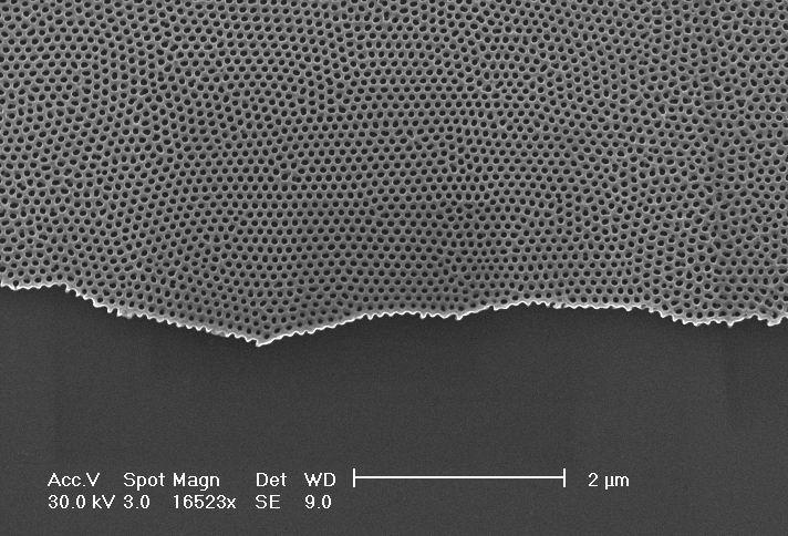
28 UTAM surface nano-patterning technique Fabrication of Highly Ordered Nanoparticle Arrays Using Ultra-thin Alumina Mask (UTAM) Motivation Use ultra-thin ordered porous alumina as evaporation or etching masks, and transfer the regularity of the pore arrays to the nanostructure arrays on substrates.
29 Fabrication process Fabricating ultra-thin alumina masks (UTAM) on Al foils and then mounting them onto the surface of silicon wafers First alumina layer Al Si foil wafer Ultra-thin Second alumina layer mask
30
31 Fabrication of the nanodot arrays Ultra-thin Nanoparticle alumina array mask Si wafer

32 CdS replicated mask Alumina CdS nanodots Highly ordered CdS nanodot arrays, UTAMs and CdS top layer on the surface of the UTAM.


33 Nanodots (top view, Pd) Nanoholes (top view, Si)
34 Tuning of the shapes and sizes of UTAM-prepared nanostructures To control the structural parameters (shape, size and spacing) is very important Controllable sizes and shapes: The pore diameters of the UTAMs can be adjusted from about 10 to 400 nm to yield nanoparticles of corresponding size. Nanometer-sized discs, hemispheres, hemi-ellipsoids, and conics (by changing the aspect ratio of the pores of the UTAMs, and the amount of material deposited through the UTAMs).


35 Highly ordered nano-disc arrays Highly ordered nano-disc arrays. Pore diameter, cell size and thickness of the UTAM are about 80, 105, and 160 nm, respectively. The aspect ratio of the apertures of the UTAM is about 1:2. The average height and size of the nano-discs are approximately 1.5 and 80 nm, respectively.
36 AFM Section Analysis of the nano-discs, the average height and size of the nano-discs are approximately 1.5 and 80 nm, respectively.


37 Highly ordered nano-hemisphere arrays Highly ordered nano-hemisphere arrays. Pore diameter, cell size and thickness of the UTAM are about 80, 105, and 240 nm, respectively. The aspect ratio of the apertures of the UTAM is about 1:3. The average height and base diameter of the nano-hemispheres are approximately and 75 nm, respectively.
38 AFM Section Analysis of the nano-hemisphere. To accurately reflect the shape of the nanoparticles, we used the same dimension scale for the horizontal and vertical coordinates. The average height and base diameter of the nanohemispheres are approximately and 75 nm, respectively.


39 Highly ordered nano-hemiellipsoid arrays Ordered nano-hemiellipsoid arrays. Pore diameter, cell size and thickness of the UTAM are about 80, 105, and 310 nm, respectively. The aspect ratio of the apertures of the UTAM is about 1:4. The average height and base diameter of the nano-hemiellipsoids are approximately and 65 nm, respectively.
40 AFM Section Analysis of the nano-hemiellipsoids. To accurately reflect the shape of the nanoparticles, we used the same dimension scale for the horizontal and vertical coordinates. The average height and base diameter of the nanohemiellipsoids are approximately and 65 nm, respectively.

41 Highly ordered nano-conic arrays Ordered nano-conic arrays. Pore diameter, cell size and thickness of the UTAM used in the fabrication process are about 80, 105, and 650 nm, respectively. The aspect ratio of the apertures of the UTAM is about 1:8. The average height and base diameter of the nano-conics are approximately and 60 nm, respectively.
42 AFM Section Analysis of the nano-conics. To accurately reflect the shape of the nanoparticles, we used the same dimension scale for the horizontal and vertical coordinates. The average height and base diameter of the nano-conics are approximately and 60 nm, respectively.
43 Aspect ratio and deposition duration Closure-effect Shadowing-effect Schematic outline of the shape and size adjustment of nanoparticles by changing the aspect ratio of the apertures of the UTAMs and the amount of material deposited through the UTAMs. (Y Lei, et al., Chem. Mater., 17, 580, 2005.)
44 Attractive features of the UTAM surface nano-patterning: Large pattern area (> 1cm 2 ) and high throughput; high density of the surface nanostructures ( cm -2 ); a general process to prepare different patterns (semiconductors, metals); well-defined nanostructures; low equipment costs.
45 A challenging technical point for UTAM technique to realize quantum-sized surface structures (below nm) Minimum pore diameter of UTAMs is about 10 nm impossible to synthesize surface structures smaller than 10 nm; the arrangement regularity and monodispersity of the pores are poor when the pore diameter is smaller than 20 nm; Prevents the fabrication of surface structures within or close to the quantum-sized range (below nm) using the UTAM patterning technique largely limits the investigation of the quantum confinement effect using the UTAM surface nano-patterning process.
46 Well-controlled pore-opening process to the barrier layer of UTAMs realizing pore-opening and surface nanostructures within the quantumsized range An alumina barrier layer between the pore bottom and the aluminum foil of asprepared PAMs. It has a hemispherical and scalloped geometry. Using acidic etching solutions, the barrier layer can be thinned and finally removed.
 under 25 V at 4 o C, cell-size 60 nm, pore-diameter 20")

![solution only etch on the bottom surface. (a) (b) 18.76 [nm] 20.00 [nm] 200.00 nm 500.00 x 500.](/docs-images/89/98913247/images/47-2.jpg "00 nm o min 1:1 Before etching in 5 wt% H 3 PO 4 solution (30 o C) 0.00 200.00 nm 500.00 x 500.")
47 UTAMs used in the pore-opening process were prepared using 0.3 M modulated H 2 SO 4 solutions (glycol/water: 3:2) under 25 V at 4 o C, cell-size 60 nm, pore-diameter 20 nm, barrier layer thickness 20 nm Pore-opening process was carried out using a 5 wt% H 3 PO 4 solution at 30 o C Before the etching, UTAMs were covered by a protecting PMMA layer on the top so that the H 3 PO 4 solution only etch on the bottom surface. (a) (b) [nm] [nm] nm x nm o min 1:1 Before etching in 5 wt% H 3 PO 4 solution (30 o C) nm x nm 10 mins surface 0.00 After 8 min etching in 5 wt% H 3 PO 4 solution (30 o C)
![(c) (d) 24.08 [nm] 46.16 [nm] 200.00 nm 500.00 x 500.00 nm 10min 1:1 0.](/docs-images/89/98913247/images/48-0.jpg "00 After 15 min etching in 5wt% H 3 PO 4 solution (30 o C) The pore")
 The pore")
![diameter is about 10 nm (f) 40.98 [nm] 54.12 [nm] 200.00 nm 500.00 x 500.](/docs-images/89/98913247/images/48-2.jpg "00 nm 2-24mins 0.00 200.00 nm 500.00 x 500.00 nm h20 30mins 0.")

48 (c) (d) [nm] [nm] nm x nm 10min 1: After 15 min etching in 5wt% H 3 PO 4 solution (30 o C) The pore diameter is about 5 nm (e) nm x nm 2-18mins edge 0.00 After 18 min etching in 5 wt% H 3 PO 4 solution (30 o C) The pore diameter is about 10 nm (f) [nm] [nm] nm x nm 2-24mins nm x nm h20 30mins 0.00 After 24 min etching in 5 wt% H 3 PO 4 solution (30 o C) The pore diameter is about 17 nm After 30 min etching in 5 wt% H 3 PO 4 solution (30 o C) The pore diameter is about 22 nm
49 UTAM surface nano-patterning Attractive features of the UTAM surface nano-patterning Large pattern area (> 1cm 2 ) and high throughput; high density of the surface nanostructures ( cm -2 ); a general process to prepare different patterns (semiconductors, metals); well-defined nanostructures; low equipment costs. Y. Lei, et.al., J. Am. Chem. Soc., 127, 1487, 2005; Chem. Mater., 17, 580, 2005; Chem. Mater., 16, 2757, 2004; Appl. Phys. Lett., 86, , 2005; Nanotechnology, 16, 1892, Y. Lei, et al., Progress in Materials Science, 52, 465, 2007.


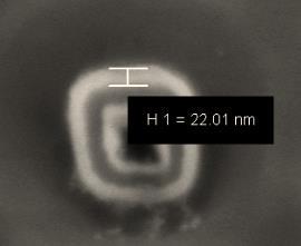
50 UTAM surface nano-patterning Barrier layer Quantum dot array 5 nm 10 nm 17 nm Small 2010, 6 (5),

51 Sub-100-nm Nanoparticle Arrays with Perfect Ordering, Tunable and Uniform Dimensions Fabricated by Combining Nanoimprinting with UTAM Technique Zhan Z.B., Lei Y., et al., ACS Nano, 8 (4), , 2014.
 UTAM transferring Al-Haddad, Lei, et al.")
52 Wafer-scale (4 in. ) UTAM transferring Al-Haddad, Lei, et al., ACS Nano, 9(8): , 2015
 UTAM transferring Perfect mounting without any")

53 Wafer-scale (4 in. ) UTAM transferring Perfect mounting without any twisting, folding, cracking and contamination A free-standing 4-in. wafer-scale UTAM with the residual Al frame Al-Haddad, Lei, et al., ACS Nano, 9(8): , 2015


54 Surface patterning using polystyrene (PS) sphere template The diameter of PS spheres can be controlled within 200 nm μm Fabrication of Ag Nanoshell Arrays S. Yang, Y. Lei, et al., Adv. Funct. Mater., 2010, 20, 2527
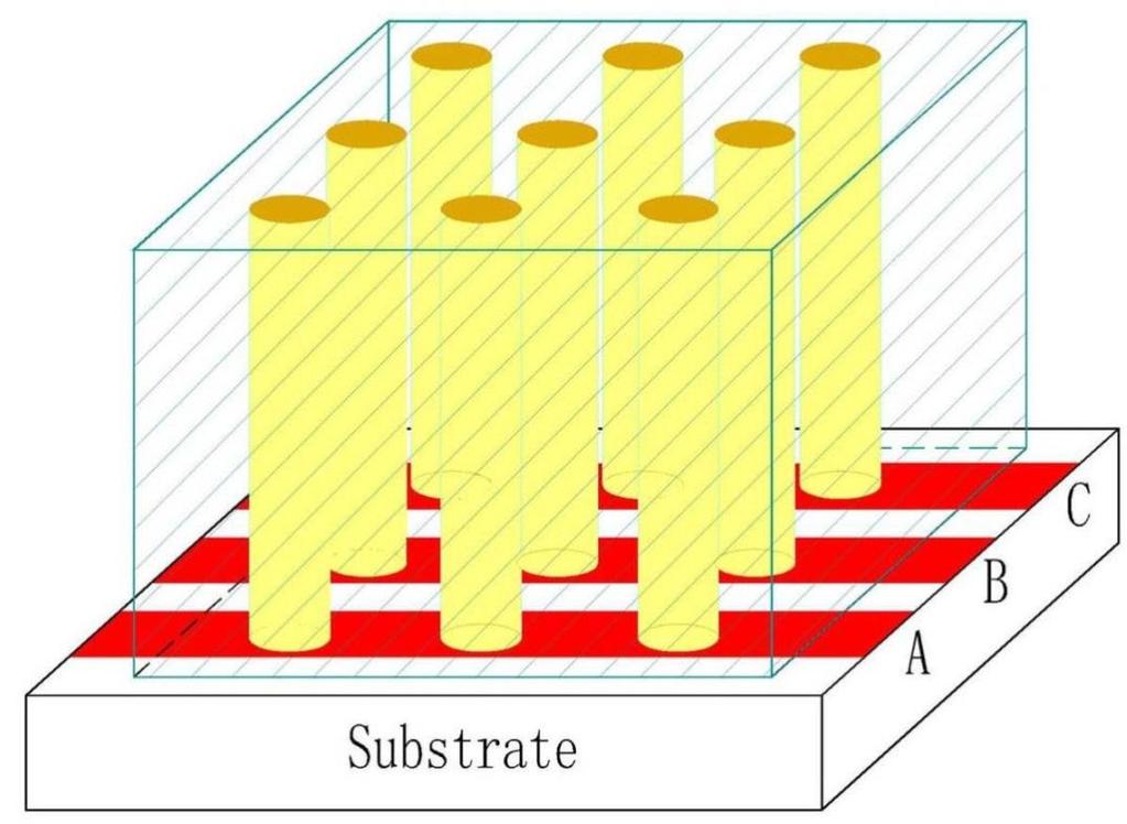
55 Three-Dimensional Surface Nano-Patterning Multifunctional surface nano-structures Dual-core CPU feature-size 45 nm From Intel Homepage, Public Relations An efficient evolution from 2-D to 3-D surface nano-patterning: Change from nanodots or nanorings to nanowires or nanotubes
56 Three-Dimensional Surface Nano-Patterning Multifunctional surface nano-structures One of the most attractive advantages of nanomaterials (extremely large surface area) is missing in the existing 2-D surface nano-patterns nanodots Only way to increase the device density is to decrease the pattern size nanorings Large contacting influence from the substrate very large signal noises degrades device performance An efficient evolution from 2-D to 3-D surface nano-patterning: Change from nanodots or nanorings to nanowires or nanotubes
57 Three-Dimensional Surface Nano-Patterning Multifunctional surface nano-structures A much larger surface area nanowires Possible to increase the device density in the lateral direction Much lower contacting influence from the substrate nanotubes An efficient evolution from 2-D to 3-D surface nano-patterning: Change from nanodots or nanorings to nanowires or nanotubes
58 From 2D to 3D surface patterns using templates Large-scale free-standing metallic nanowires for 3D surface patterns: (Left): top view of nanowire array of an area of about 775 μm 2. (Right): high regularity of nanowire arrays.


59 From 2D to 3D surface patterns using templates Large-scale free-standing metallic nanowires for 3D surface patterns: (Left): top view of nanowire array of an area of about 775 μm 2. (Right): high regularity of nanowire arrays.
")

60 Metallic nanotube arrays (by ALD) Cover almost all inner surface of AAO


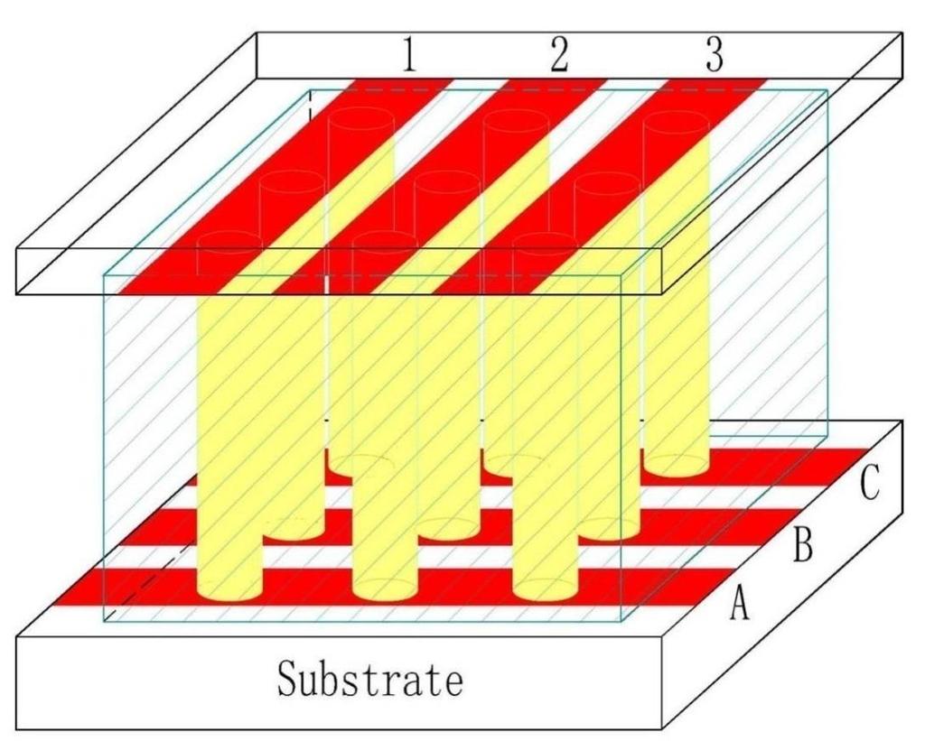
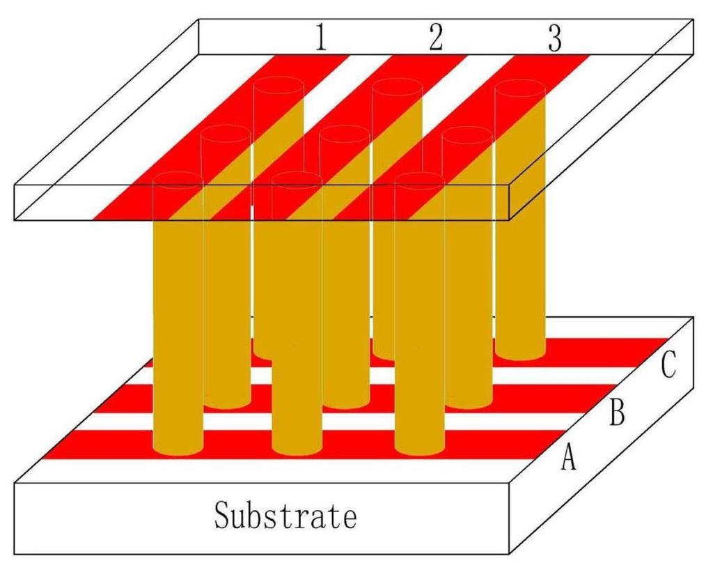
61 3D Surface Nano-Patterning: Addressing Addressing System for 3-D surface nanostructures with nano-scale resolution nanowire 1A Schematic of the addressing system (only shows an array of 3 3)

62 Addressing system
 2.")
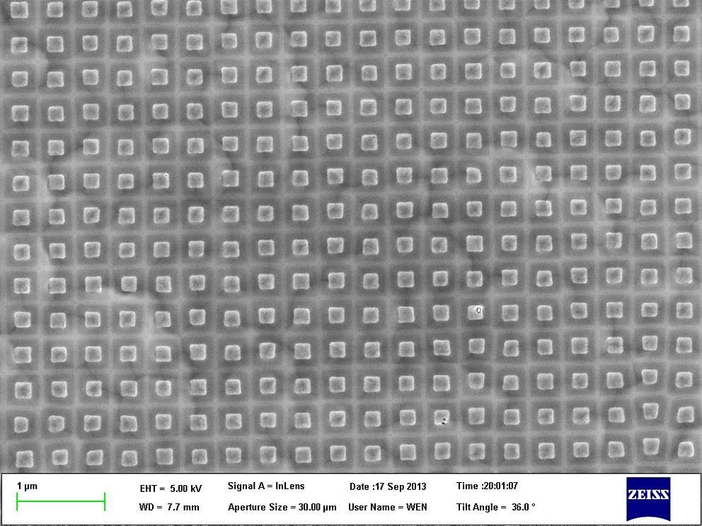
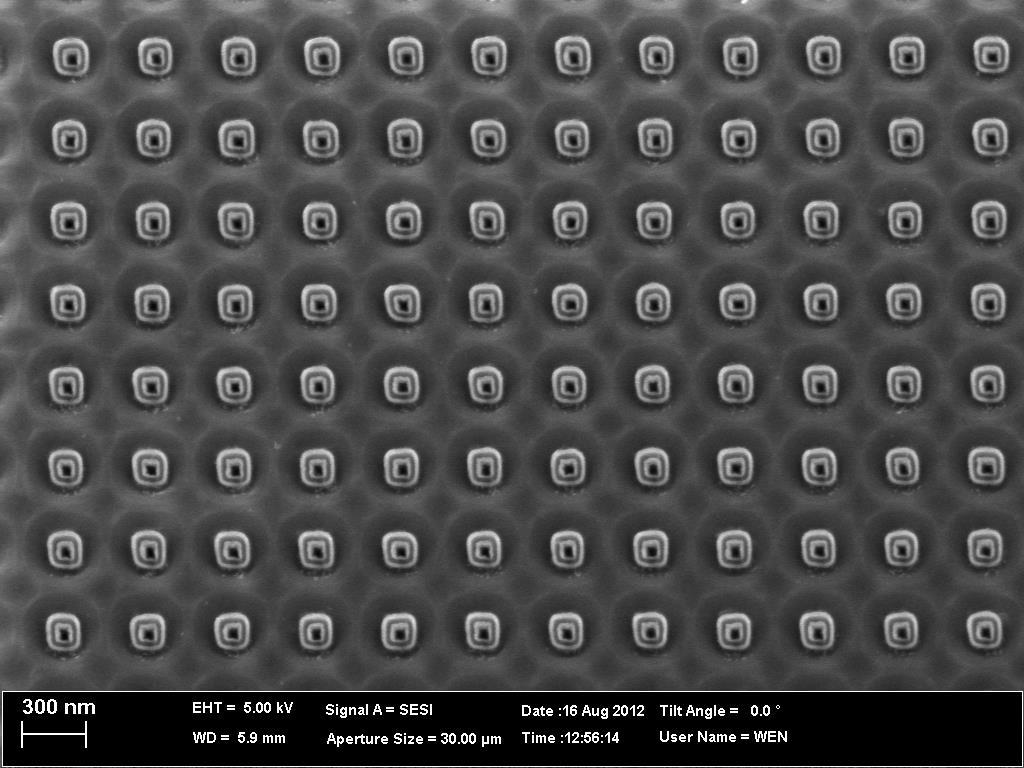
63 3D Surface Nano-Patterning: nano-templates with large-scale (up to 1 mm 2 ) perfect pore arrays without defects 1. The short-range pore regularity of UTAMs or AAO templates Template with large-scale perfect pore arrays (to mm 2 or even to cm 2 ) 2. Hexagonal pore arrangement Rectangular pore arrangement

64 Templates with large-scale (1 mm 2 ) perfect rectangular pore arrays without defect


65 Templates with large-scale (1 mm 2 ) perfect rectangular pore arrays without defect


66 TiO 2 nanotubes grown in the template (Before removing template)
67


68 Addressing system Focus Ion Beam Lithography Visual operation Drawback: 1. Time consuming. 2. The pattern area is too small to the semiconductor process.


69 Addressing system Alignment between the top of nanowire and the electrode lines.


70 Addressing system We success realizing perfect match between the top of nanowire and the electrode lines!


71 Addressing system Then, how to realizing the backside electrode lines? Glass or Si PDMS Al Al PDMS Glass or Si
72 Addressing system New process- a metal supporting layer Ag 10 um Ag 200 nm Al Al Ag 200 nm Ag 10 um


73 Addressing system How to match the both side electrode lines as we design???? Front side Back side

74 Addressing system We success realizing good matching between the top and bottom electrode lines!!!

75 Addressing system We success realizing good matching between the top and bottom electrode lines!!!
76 Thank you and have a nice day!
Techniken der Oberflächenphysik (Technique of Surface Physics)
") Techniken der Oberflächenphysik (Technique of Surface Physics) Yong Lei & Fabian Grote Fachgebiet 3D-Nanostrukturierung, Institut für Physik Contact: yong.lei@tu-ilmenau.de; fabian.grote@tu-ilmenau.de
Techniken der Oberflächenphysik (Technique of Surface Physics) Yong Lei & Fabian Grote Fachgebiet 3D-Nanostrukturierung, Institut für Physik Contact: yong.lei@tu-ilmenau.de; fabian.grote@tu-ilmenau.de
Nanostrukturphysik (Nanostructure Physics)
") Nanostrukturphysik (Nanostructure Physics) Prof. Yong Lei & Dr. Yang Xu Fachgebiet 3D-Nanostrukturierung, Institut für Physik Contact: yong.lei@tu-ilmenau.de; yang.xu@tu-ilmenau.de Office: Unterpoerlitzer
Nanostrukturphysik (Nanostructure Physics) Prof. Yong Lei & Dr. Yang Xu Fachgebiet 3D-Nanostrukturierung, Institut für Physik Contact: yong.lei@tu-ilmenau.de; yang.xu@tu-ilmenau.de Office: Unterpoerlitzer
Techniken der Oberflächenphysik (Techniques of Surface Physics)
") Techniken der Oberflächenphysik (Techniques of Surface Physics) Prof. Yong Lei & Dr. Yang Xu Fachgebiet 3D-Nanostrukturierung, Institut für Physik Contact: yong.lei@tu-ilmenau.de yang.xu@tu-ilmenau.de
Techniken der Oberflächenphysik (Techniques of Surface Physics) Prof. Yong Lei & Dr. Yang Xu Fachgebiet 3D-Nanostrukturierung, Institut für Physik Contact: yong.lei@tu-ilmenau.de yang.xu@tu-ilmenau.de
Nanostrukturphysik (Nanostructure Physics)
") Nanostrukturphysik (Nanostructure Physics) Yong Lei & Fabian Grote Fachgebiet 3D-Nanostrukturierung, Institut für Physik Contact: yong.lei@tu-ilmenau.de; fabian.grote@tu-ilmenau.de Office: Heliosbau 1102,
Nanostrukturphysik (Nanostructure Physics) Yong Lei & Fabian Grote Fachgebiet 3D-Nanostrukturierung, Institut für Physik Contact: yong.lei@tu-ilmenau.de; fabian.grote@tu-ilmenau.de Office: Heliosbau 1102,
Nanostrukturphysik (Nanostructure Physics)
") Nanostrukturphysik (Nanostructure Physics) Prof. Yong Lei & Dr. Huaping Zhao Fachgebiet Angewandte Nanophysik, Institut für Physik Contact: yong.lei@tu-ilmenau.de; huaping.zhao@tu-ilmenau.de Office: Unterpoerlitzer
Nanostrukturphysik (Nanostructure Physics) Prof. Yong Lei & Dr. Huaping Zhao Fachgebiet Angewandte Nanophysik, Institut für Physik Contact: yong.lei@tu-ilmenau.de; huaping.zhao@tu-ilmenau.de Office: Unterpoerlitzer
Techniken der Oberflächenphysik (Techniques of Surface Physics)
") Techniken der Oberflächenphysik (Techniques of Surface Physics) Prof. Yong Lei Dr. Ynag Xu and Mr. Grote Fabian Fachgebiet 3D-Nanostrukturierung, Institut für Physik Contact: yong.lei@tu-ilmenau.de; yang.xu@tu-ilmenau.de
Techniken der Oberflächenphysik (Techniques of Surface Physics) Prof. Yong Lei Dr. Ynag Xu and Mr. Grote Fabian Fachgebiet 3D-Nanostrukturierung, Institut für Physik Contact: yong.lei@tu-ilmenau.de; yang.xu@tu-ilmenau.de
Nanostrukturphysik (Nanostructure Physics)
") Nanostrukturphysik (Nanostructure Physics) Prof. Yong Lei & Dr. Yang Xu Fachgebiet 3D-Nanostrukturierung, Institut für Physik Contact: yong.lei@tu-ilmenau.de; yang.xu@tu-ilmenau.de Office: Unterpoerlitzer
Nanostrukturphysik (Nanostructure Physics) Prof. Yong Lei & Dr. Yang Xu Fachgebiet 3D-Nanostrukturierung, Institut für Physik Contact: yong.lei@tu-ilmenau.de; yang.xu@tu-ilmenau.de Office: Unterpoerlitzer
Halbleiter Prof. Yong Lei Prof. Thomas Hannappel
 Halbleiter Prof. Yong Lei Prof. Thomas Hannappel yong.lei@tu-ilmenau.de thomas.hannappel@tu-ilmenau.de http:///nanostruk/ Organic semiconductors Small-molecular materials Rubrene Pentacene Polymers PEDOT:PSS
Techniken der Oberflächenphysik (Techniques of Surface Physics)
") Techniken der Oberflächenphysik (Techniques of Surface Physics) Prof. Yong Lei & Dr. Yang Xu (& Liying Liang) Fachgebiet 3D-Nanostrukturierung, Institut für Physik Contact: yong.lei@tu-ilmenau.de; yang.xu@tu-ilmenau.de;
Techniken der Oberflächenphysik (Techniques of Surface Physics) Prof. Yong Lei & Dr. Yang Xu (& Liying Liang) Fachgebiet 3D-Nanostrukturierung, Institut für Physik Contact: yong.lei@tu-ilmenau.de; yang.xu@tu-ilmenau.de;
From nanophysics research labs to cell phones. Dr. András Halbritter Department of Physics associate professor
 From nanophysics research labs to cell phones Dr. András Halbritter Department of Physics associate professor Curriculum Vitae Birth: 1976. High-school graduation: 1994. Master degree: 1999. PhD: 2003.
Chapter 10. Nanometrology. Oxford University Press All rights reserved.
 Chapter 10 Nanometrology Oxford University Press 2013. All rights reserved. 1 Introduction Nanometrology is the science of measurement at the nanoscale level. Figure illustrates where nanoscale stands
Nanostrukturphysik (Nanostructure Physics)
") Nanostrukturphysik (Nanostructure Physics) Prof. Yong Lei & Dr. Yang Xu Fachgebiet 3D-Nanostrukturierung, Institut für Physik Contact: yong.lei@tu-ilmenau.de; yang.xu@tu-ilmenau.de Office: Unterpoerlitzer
Nanostrukturphysik (Nanostructure Physics) Prof. Yong Lei & Dr. Yang Xu Fachgebiet 3D-Nanostrukturierung, Institut für Physik Contact: yong.lei@tu-ilmenau.de; yang.xu@tu-ilmenau.de Office: Unterpoerlitzer
High-resolution Characterization of Organic Ultrathin Films Using Atomic Force Microscopy
 High-resolution Characterization of Organic Ultrathin Films Using Atomic Force Microscopy Jing-jiang Yu Nanotechnology Measurements Division Agilent Technologies, Inc. Atomic Force Microscopy High-Resolution
Halbleiter. Prof. Yong Lei. Prof. Thomas Hannappel.
 Halbleiter Prof. Yong Lei Prof. Thomas Hannappel yong.lei@tu-ilemnau.de thomas.hannappel@tu-ilmenau.de Important Events in Semiconductors History 1833 Michael Faraday discovered temperature-dependent conductivity
SUPPLEMENTARY INFORMATION
 In the format provided by the authors and unedited. DOI: 10.1038/NNANO.2016.257 Multiple nanostructures based on anodized aluminium oxide templates Liaoyong Wen, Rui Xu, Yan Mi, Yong Lei * 1 NATURE NANOTECHNOLOGY
Nanostrukturphysik Übung 2 (Class 3&4)
") Nanostrukturphysik Übung 2 (Class 3&4) Prof. Yong Lei & Dr. Yang Xu 2017.05.03 Fachgebiet 3D-Nanostrukturierung, Institut für Physik Contact: yong.lei@tu-ilmenau.de (3748), yang.xu@tuilmenau.de (4902)
Nanostrukturphysik Übung 2 (Class 3&4) Prof. Yong Lei & Dr. Yang Xu 2017.05.03 Fachgebiet 3D-Nanostrukturierung, Institut für Physik Contact: yong.lei@tu-ilmenau.de (3748), yang.xu@tuilmenau.de (4902)
Chapter 12. Nanometrology. Oxford University Press All rights reserved.
 Chapter 12 Nanometrology Introduction Nanometrology is the science of measurement at the nanoscale level. Figure illustrates where nanoscale stands in relation to a meter and sub divisions of meter. Nanometrology
EN2912C: Future Directions in Computing Lecture 08: Overview of Near-Term Emerging Computing Technologies
 EN2912C: Future Directions in Computing Lecture 08: Overview of Near-Term Emerging Computing Technologies Prof. Sherief Reda Division of Engineering Brown University Fall 2008 1 Near-term emerging computing
MS482 Materials Characterization ( 재료분석 ) Lecture Note 11: Scanning Probe Microscopy. Byungha Shin Dept. of MSE, KAIST
 Lecture Note 11: Scanning Probe Microscopy. Byungha Shin Dept. of MSE, KAIST") 2015 Fall Semester MS482 Materials Characterization ( 재료분석 ) Lecture Note 11: Scanning Probe Microscopy Byungha Shin Dept. of MSE, KAIST 1 Course Information Syllabus 1. Overview of various characterization
2015 Fall Semester MS482 Materials Characterization ( 재료분석 ) Lecture Note 11: Scanning Probe Microscopy Byungha Shin Dept. of MSE, KAIST 1 Course Information Syllabus 1. Overview of various characterization
Nanostrukturphysik. Prof. Yong Lei & Dr. Yang Xu Fachgebiet 3D-Nanostrukturierung, Institut für Physik
 Nanostrukturphysik Prof. Yong Lei & Dr. Yang Xu Fachgebiet 3D-Nanostrukturierung, Institut für Physik Contact: yong.lei@tu-ilmenau.de (3748), yang.xu@tuilmenau.de (4902) Office: Gebäude V202, Unterpörlitzer
Initial Stages of Growth of Organic Semiconductors on Graphene
 Initial Stages of Growth of Organic Semiconductors on Graphene Presented by: Manisha Chhikara Supervisor: Prof. Dr. Gvido Bratina University of Nova Gorica Outline Introduction to Graphene Fabrication
Carbon based Nanoscale Electronics
 Carbon based Nanoscale Electronics 09 02 200802 2008 ME class Outline driving force for the carbon nanomaterial electronic properties of fullerene exploration of electronic carbon nanotube gold rush of
performance electrocatalytic or electrochemical devices. Nanocrystals grown on graphene could have
 Nanocrystal Growth on Graphene with Various Degrees of Oxidation Hailiang Wang, Joshua Tucker Robinson, Georgi Diankov, and Hongjie Dai * Department of Chemistry and Laboratory for Advanced Materials,
Fabrication at the nanoscale for nanophotonics
 Fabrication at the nanoscale for nanophotonics Ilya Sychugov, KTH Materials Physics, Kista silicon nanocrystal by electron beam induced deposition lithography Outline of basic nanofabrication methods Devices
Graphene films on silicon carbide (SiC) wafers supplied by Nitride Crystals, Inc.
 wafers supplied by Nitride Crystals, Inc.") 9702 Gayton Road, Suite 320, Richmond, VA 23238, USA Phone: +1 (804) 709-6696 info@nitride-crystals.com www.nitride-crystals.com Graphene films on silicon carbide (SiC) wafers supplied by Nitride Crystals,
9702 Gayton Road, Suite 320, Richmond, VA 23238, USA Phone: +1 (804) 709-6696 info@nitride-crystals.com www.nitride-crystals.com Graphene films on silicon carbide (SiC) wafers supplied by Nitride Crystals,
Nanostructure. Materials Growth Characterization Fabrication. More see Waser, chapter 2
 Nanostructure Materials Growth Characterization Fabrication More see Waser, chapter 2 Materials growth - deposition deposition gas solid Physical Vapor Deposition Chemical Vapor Deposition Physical Vapor
General concept and defining characteristics of AFM. Dina Kudasheva Advisor: Prof. Mary K. Cowman
 General concept and defining characteristics of AFM Dina Kudasheva Advisor: Prof. Mary K. Cowman Overview Introduction History of the SPM invention Technical Capabilities Principles of operation Examples
Nanotechnology. Yung Liou P601 Institute of Physics Academia Sinica
 Nanotechnology Yung Liou P601 yung@phys.sinica.edu.tw Institute of Physics Academia Sinica 1 1st week Definition of Nanotechnology The Interagency Subcommittee on Nanoscale Science, Engineering and Technology
CHARACTERIZATION of NANOMATERIALS KHP
 CHARACTERIZATION of NANOMATERIALS Overview of the most common nanocharacterization techniques MAIN CHARACTERIZATION TECHNIQUES: 1.Transmission Electron Microscope (TEM) 2. Scanning Electron Microscope
Nanostructure Fabrication Using Selective Growth on Nanosize Patterns Drawn by a Scanning Probe Microscope
 Nanostructure Fabrication Using Selective Growth on Nanosize Patterns Drawn by a Scanning Probe Microscope Kentaro Sasaki, Keiji Ueno and Atsushi Koma Department of Chemistry, The University of Tokyo,
There's Plenty of Room at the Bottom
 There's Plenty of Room at the Bottom 12/29/1959 Feynman asked why not put the entire Encyclopedia Britannica (24 volumes) on a pin head (requires atomic scale recording). He proposed to use electron microscope
Unconventional Nano-patterning. Peilin Chen
 Unconventional Nano-patterning Peilin Chen Reference Outlines History of patterning Traditional Nano-patterning Unconventional Nano-patterning Ancient Patterning "This is the Elks' land". A greeting at
ESH Benign Processes for he Integration of Quantum Dots (QDs)
") ESH Benign Processes for he Integration of Quantum Dots (QDs) PIs: Karen K. Gleason, Department of Chemical Engineering, MIT Graduate Students: Chia-Hua Lee: PhD Candidate, Department of Material Science
ESH Benign Processes for he Integration of Quantum Dots (QDs) PIs: Karen K. Gleason, Department of Chemical Engineering, MIT Graduate Students: Chia-Hua Lee: PhD Candidate, Department of Material Science
Seminars in Nanosystems - I
 Seminars in Nanosystems - I Winter Semester 2011/2012 Dr. Emanuela Margapoti Emanuela.Margapoti@wsi.tum.de Dr. Gregor Koblmüller Gregor.Koblmueller@wsi.tum.de Seminar Room at ZNN 1 floor Topics of the
Graphene. Tianyu Ye November 30th, 2011
 Graphene Tianyu Ye November 30th, 2011 Outline What is graphene? How to make graphene? (Exfoliation, Epitaxial, CVD) Is it graphene? (Identification methods) Transport properties; Other properties; Applications;
Kavli Workshop for Journalists. June 13th, CNF Cleanroom Activities
 Kavli Workshop for Journalists June 13th, 2007 CNF Cleanroom Activities Seeing nm-sized Objects with an SEM Lab experience: Scanning Electron Microscopy Equipment: Zeiss Supra 55VP Scanning electron microscopes
Introduction to Nanotechnology Chapter 5 Carbon Nanostructures Lecture 1
 Introduction to Nanotechnology Chapter 5 Carbon Nanostructures Lecture 1 ChiiDong Chen Institute of Physics, Academia Sinica chiidong@phys.sinica.edu.tw 02 27896766 Section 5.2.1 Nature of the Carbon Bond
Imaging Methods: Scanning Force Microscopy (SFM / AFM)
") Imaging Methods: Scanning Force Microscopy (SFM / AFM) The atomic force microscope (AFM) probes the surface of a sample with a sharp tip, a couple of microns long and often less than 100 Å in diameter.
Imaging Methods: Scanning Force Microscopy (SFM / AFM) The atomic force microscope (AFM) probes the surface of a sample with a sharp tip, a couple of microns long and often less than 100 Å in diameter.
Large-Area and Uniform Surface-Enhanced Raman. Saturation
 Supporting Information Large-Area and Uniform Surface-Enhanced Raman Spectroscopy Substrate Optimized by Enhancement Saturation Daejong Yang 1, Hyunjun Cho 2, Sukmo Koo 1, Sagar R. Vaidyanathan 2, Kelly
29: Nanotechnology. What is Nanotechnology? Properties Control and Understanding. Nanomaterials
 29: Nanotechnology What is Nanotechnology? Properties Control and Understanding Nanomaterials Making nanomaterials Seeing at the nanoscale Quantum Dots Carbon Nanotubes Biology at the Nanoscale Some Applications
Graphene Fundamentals and Emergent Applications
 Graphene Fundamentals and Emergent Applications Jamie H. Warner Department of Materials University of Oxford Oxford, UK Franziska Schaffel Department of Materials University of Oxford Oxford, UK Alicja
Wafer-scale fabrication of graphene
 Wafer-scale fabrication of graphene Sten Vollebregt, MSc Delft University of Technology, Delft Institute of Mircosystems and Nanotechnology Delft University of Technology Challenge the future Delft University
Surface Studies by Scanning Tunneling Microscopy
 Surface Studies by Scanning Tunneling Microscopy G. Binnig, H. Rohrer, Ch. Gerber, and E. Weibel IBM Zurich Research Laboratory, 8803 Ruschlikon-ZH, Switzerland (Received by Phys. Rev. Lett. on 30th April,
Supplementary information
 Supplementary information Electrochemical synthesis of metal and semimetal nanotube-nanowire heterojunctions and their electronic transport properties Dachi Yang, ab Guowen Meng,* a Shuyuan Zhang, c Yufeng
Introduction to Nanotechnology Chapter 5 Carbon Nanostructures Lecture 1
 Introduction to Nanotechnology Chapter 5 Carbon Nanostructures Lecture 1 ChiiDong Chen Institute of Physics, Academia Sinica chiidong@phys.sinica.edu.tw 02 27896766 Carbon contains 6 electrons: (1s) 2,
D DAVID PUBLISHING. Study the Synthesis Parameter of Tin Oxide Nanostructure. 1. Introduction. 2. Experiment
 Journal of Materials Science and Engineering B 5 (9-10) (2015) 353-360 doi: 10.17265/2161-6221/2015.9-10.003 D DAVID PUBLISHING Study the Synthesis Parameter of Tin Oxide Nanostructure Gyanendra Prakash
Carbon Structure Simulations using Crystal Viewer Tool
 Carbon Structure Simulations using Crystal Viewer Tool The Crystal Viewer tool in nanohub.org can be used to build three carbon nanostructures: graphene sheets, Buckminsterfullerene, Bucky balls (C 60
EE 527 MICROFABRICATION. Lecture 5 Tai-Chang Chen University of Washington
 EE 527 MICROFABRICATION Lecture 5 Tai-Chang Chen University of Washington MICROSCOPY AND VISUALIZATION Electron microscope, transmission electron microscope Resolution: atomic imaging Use: lattice spacing.
CVD growth of Graphene. SPE ACCE presentation Carter Kittrell James M. Tour group September 9 to 11, 2014
 CVD growth of Graphene SPE ACCE presentation Carter Kittrell James M. Tour group September 9 to 11, 2014 Graphene zigzag armchair History 1500: Pencil-Is it made of lead? 1789: Graphite 1987: The first
A Novel Self-aligned and Maskless Process for Formation of Highly Uniform Arrays of Nanoholes and Nanopillars
 Nanoscale Res Lett (2008) 3: 127 DOI 10.1007/s11671-008-9124-6 NANO EXPRESS A Novel Self-aligned and Maskless Process for Formation of Highly Uniform Arrays of Nanoholes and Nanopillars Wei Wu Æ Dibyendu
1-amino-9-octadecene, HAuCl 4, hexane, ethanol 55 o C, 16h AuSSs on GO
 Supplementary Figures GO Supplementary Figure S1 1-amino-9-octadecene, HAuCl 4, hexane, ethanol 55 o C, 16h AuSSs on GO Schematic illustration of synthesis of Au square sheets on graphene oxide sheets.
3-month progress Report
 3-month progress Report Graphene Devices and Circuits Supervisor Dr. P.A Childs Table of Content Abstract... 1 1. Introduction... 1 1.1 Graphene gold rush... 1 1.2 Properties of graphene... 3 1.3 Semiconductor
Materials. Definitions of nanotechnology. The term nanotechnology was invented by Professor Norio Taniguchi at the University of Tokyo in 1971.
 Materials Definitions of nanotechnology The term nanotechnology was invented by Professor Norio Taniguchi at the University of Tokyo in 1971. The original definition, translated into English Nano-technology'
Overview. Carbon in all its forms. Background & Discovery Fabrication. Important properties. Summary & References. Overview of current research
 Graphene Prepared for Solid State Physics II Pr Dagotto Spring 2009 Laurene Tetard 03/23/09 Overview Carbon in all its forms Background & Discovery Fabrication Important properties Overview of current
Nanotechnology. Gavin Lawes Department of Physics and Astronomy
 Nanotechnology Gavin Lawes Department of Physics and Astronomy Earth-Moon distance 4x10 8 m (courtesy NASA) Length scales (Part I) Person 2m Magnetic nanoparticle 5x10⁻⁹ m 10 10 m 10 5 m 1 m 10-5 m 10-10
Nanoelectronics 09. Atsufumi Hirohata Department of Electronics. Quick Review over the Last Lecture
 Nanoelectronics 09 Atsufumi Hirohata Department of Electronics 13:00 Monday, 12/February/2018 (P/T 006) Quick Review over the Last Lecture ( Field effect transistor (FET) ): ( Drain ) current increases
Carbon nanomaterials. Gavin Lawes Wayne State University.
 Carbon nanomaterials Gavin Lawes Wayne State University glawes@wayne.edu Outline 1. Carbon structures 2. Carbon nanostructures 3. Potential applications for Carbon nanostructures Periodic table from bpc.edu
Physics and Material Science of Semiconductor Nanostructures
 Physics and Material Science of Semiconductor Nanostructures PHYS 570P Prof. Oana Malis Email: omalis@purdue.edu Course website: http://www.physics.purdue.edu/academic_programs/courses/phys570p/ 1 Course
Carbon Nanomaterials: Nanotubes and Nanobuds and Graphene towards new products 2030
 Carbon Nanomaterials: Nanotubes and Nanobuds and Graphene towards new products 2030 Prof. Dr. Esko I. Kauppinen Helsinki University of Technology (TKK) Espoo, Finland Forecast Seminar February 13, 2009
Nanotechnology Nanofabrication of Functional Materials. Marin Alexe Max Planck Institute of Microstructure Physics, Halle - Germany
 Nanotechnology Nanofabrication of Functional Materials Marin Alexe Max Planck Institute of Microstructure Physics, Halle - Germany Contents Part I History and background to nanotechnology Nanoworld Nanoelectronics
Scanning Probe Microscopy. EMSE-515 F. Ernst
 Scanning Probe Microscopy EMSE-515 F. Ernst 1 Literature 2 3 Scanning Probe Microscopy: The Lab on a Tip by Ernst Meyer,Ans Josef Hug,Roland Bennewitz 4 Scanning Probe Microscopy and Spectroscopy : Theory,
Title of file for HTML: Supplementary Information Description: Supplementary Figures and Supplementary References
 Title of file for HTML: Supplementary Information Description: Supplementary Figures and Supplementary References Supplementary Figure 1. SEM images of perovskite single-crystal patterned thin film with
Surface atoms/molecules of a material act as an interface to its surrounding environment;
 1 Chapter 1 Thesis Overview Surface atoms/molecules of a material act as an interface to its surrounding environment; their properties are often complicated by external adsorbates/species on the surface
In the name of Allah
 In the name of Allah Nano chemistry- 4 th stage Lecture No. 1 History of nanotechnology 16-10-2016 Assistance prof. Dr. Luma Majeed Ahmed lumamajeed2013@gmail.com, luma.ahmed@uokerbala.edu.iq Nano chemistry-4
Electrochemically Synthesized Multi-block
 Electrochemically Synthesized Multi-block Nanorods Sungho Park SungKyunKwan University, Department of Chemistry & SKKU Advanced Institute of Nanotechnology (SAINT) J. Am. Chem. Soc. 2003, 125, 2282-2290
In today s lecture, we will cover:
 In today s lecture, we will cover: Metal and Metal oxide Nanoparticles Semiconductor Nanocrystals Carbon Nanotubes 1 Week 2: Nanoparticles Goals for this section Develop an understanding of the physical
MSN551 LITHOGRAPHY II
 MSN551 Introduction to Micro and Nano Fabrication LITHOGRAPHY II E-Beam, Focused Ion Beam and Soft Lithography Why need electron beam lithography? Smaller features are required By electronics industry:
The goal of this project is to enhance the power density and lowtemperature efficiency of solid oxide fuel cells (SOFC) manufactured by atomic layer
 manufactured by atomic layer") Stanford University Michael Shandalov1, Shriram Ramanathan2, Changhyun Ko2 and Paul McIntyre1 1Department of Materials Science and Engineering, Stanford University 2Division of Engineering and Applied
Stanford University Michael Shandalov1, Shriram Ramanathan2, Changhyun Ko2 and Paul McIntyre1 1Department of Materials Science and Engineering, Stanford University 2Division of Engineering and Applied
Graphene Novel Material for Nanoelectronics
 Graphene Novel Material for Nanoelectronics Shintaro Sato Naoki Harada Daiyu Kondo Mari Ohfuchi (Manuscript received May 12, 2009) Graphene is a flat monolayer of carbon atoms with a two-dimensional honeycomb
Nanomaterials and their Optical Applications
 Nanomaterials and their Optical Applications Winter Semester 2013 Lecture 02 rachel.grange@uni-jena.de http://www.iap.uni-jena.de/multiphoton Lecture 2: outline 2 Introduction to Nanophotonics Theoretical
materials, devices and systems through manipulation of matter at nanometer scale and exploitation of novel phenomena which arise because of the
 Nanotechnology is the creation of USEFUL/FUNCTIONAL materials, devices and systems through manipulation of matter at nanometer scale and exploitation of novel phenomena which arise because of the nanometer
MS482 Materials Characterization ( 재료분석 ) Lecture Note 12: Summary. Byungha Shin Dept. of MSE, KAIST
 Lecture Note 12: Summary. Byungha Shin Dept. of MSE, KAIST") 2015 Fall Semester MS482 Materials Characterization ( 재료분석 ) Lecture Note 12: Summary Byungha Shin Dept. of MSE, KAIST 1 Course Information Syllabus 1. Overview of various characterization techniques (1
2015 Fall Semester MS482 Materials Characterization ( 재료분석 ) Lecture Note 12: Summary Byungha Shin Dept. of MSE, KAIST 1 Course Information Syllabus 1. Overview of various characterization techniques (1
Solutions for Assignment-8
 Solutions for Assignment-8 Q1. The process of adding impurities to a pure semiconductor is called: [1] (a) Mixing (b) Doping (c) Diffusing (d) None of the above In semiconductor production, doping intentionally
Revealing High Fidelity of Nanomolding Process by Extracting the Information from AFM Image with Systematic Artifacts
 Revealing High Fidelity of Nanomolding Process by Extracting the Information from AFM Image with Systematic Artifacts Sajal Biring* Department of Electronics Engineering and Organic Electronics Research
2D Materials for Gas Sensing
 2D Materials for Gas Sensing S. Guo, A. Rani, and M.E. Zaghloul Department of Electrical and Computer Engineering The George Washington University, Washington DC 20052 Outline Background Structures of
Imaging Carbon materials with correlative Raman-SEM microscopy. Introduction. Raman, SEM and FIB within one chamber. Diamond.
 Imaging Carbon materials with correlative Raman-SEM microscopy Application Example Carbon materials are widely used in many industries for their exceptional properties. Electric conductance, light weight,
1. Nanotechnology & nanomaterials -- Functional nanomaterials enabled by nanotechnologies.
 Novel Nano-Engineered Semiconductors for Possible Photon Sources and Detectors NAI-CHANG YEH Department of Physics, California Institute of Technology 1. Nanotechnology & nanomaterials -- Functional nanomaterials
TRANSVERSE SPIN TRANSPORT IN GRAPHENE
 International Journal of Modern Physics B Vol. 23, Nos. 12 & 13 (2009) 2641 2646 World Scientific Publishing Company TRANSVERSE SPIN TRANSPORT IN GRAPHENE TARIQ M. G. MOHIUDDIN, A. A. ZHUKOV, D. C. ELIAS,
Final Reading Assignment: Travels to the Nanoworld: pages pages pages
 Final Reading Assignment: Travels to the Nanoworld: pages 152-164 pages 201-214 pages 219-227 Bottom-up nanofabrication Can we assemble nanomachines manually? What are the components (parts)? nanoparticles
III-V nanostructured materials synthesized by MBE droplet epitaxy
 III-V nanostructured materials synthesized by MBE droplet epitaxy E.A. Anyebe 1, C. C. Yu 1, Q. Zhuang 1,*, B. Robinson 1, O Kolosov 1, V. Fal ko 1, R. Young 1, M Hayne 1, A. Sanchez 2, D. Hynes 2, and
School of Chemical and Biological Engineering, College of Engineering, Seoul National University, 599 Gwanangno, Gwanakgu, Seoul , Korea ACS
 School of Chemical and Biological Engineering, College of Engineering, Seoul National University, 599 Gwanangno, Gwanakgu, Seoul 151-742, Korea ACS Appl. Mater. Interfaces 2015, 7, 1746 1751 (DOI: 10.1021/am507314t)
Scanning Probe Microscopy. Amanda MacMillan, Emmy Gebremichael, & John Shamblin Chem 243: Instrumental Analysis Dr. Robert Corn March 10, 2010
 Scanning Probe Microscopy Amanda MacMillan, Emmy Gebremichael, & John Shamblin Chem 243: Instrumental Analysis Dr. Robert Corn March 10, 2010 Scanning Probe Microscopy High-Resolution Surface Analysis
Südliche Stadtmauerstr. 15a Tel: D Erlangen Fax:
 Curriculum Vitae Lionel Santinacci 19.10.1974 Nationality: French Südliche Stadtmauerstr. 15a Tel: + 49 9131 852 7587 D-91054 Erlangen Fax: + 49 9131 852 7582 Germany e-mail: lionel@ww.uni-erlangen.de
1.0 Introduction. 1.1 Nanotechnology Historical Developments
 1.0 Introduction 1.1 Nanotechnology Historical Developments Around 370BC, Democritus a Greek philosopher developed the atomic theory of matter. Nano in GREEK means DWARF. The prefix nano means a billionth
Fabrication Methods: Chapter 4. Often two methods are typical. Top Down Bottom up. Begins with atoms or molecules. Begins with bulk materials
 Fabrication Methods: Chapter 4 Often two methods are typical Top Down Bottom up Begins with bulk materials Begins with atoms or molecules Reduced in size to nano By thermal, physical Chemical, electrochemical
Auger Electron Spectroscopy Overview
 Auger Electron Spectroscopy Overview Also known as: AES, Auger, SAM 1 Auger Electron Spectroscopy E KLL = E K - E L - E L AES Spectra of Cu EdN(E)/dE Auger Electron E N(E) x 5 E KLL Cu MNN Cu LMM E f E
There s plenty of room at the bottom! - R.P. Feynman, Nanostructure: a piece of material with at least one dimension less than 100 nm in extent.
 Nanostructures and Nanotechnology There s plenty of room at the bottom! - R.P. Feynman, 1959 Materials behave differently when structured at the nm scale than they do in bulk. Technologies now exist that
Low Voltage Field Emission SEM (LV FE-SEM): A Promising Imaging Approach for Graphene Samples
: A Promising Imaging Approach for Graphene Samples") Low Voltage Field Emission SEM (LV FE-SEM): A Promising Imaging Approach for Graphene Samples Jining Xie Agilent Technologies May 23 rd, 2012 www.agilent.com/find/nano Outline 1. Introduction 2. Agilent
Low Voltage Field Emission SEM (LV FE-SEM): A Promising Imaging Approach for Graphene Samples Jining Xie Agilent Technologies May 23 rd, 2012 www.agilent.com/find/nano Outline 1. Introduction 2. Agilent
MSE 321 Structural Characterization
 Auger Spectroscopy Auger Electron Spectroscopy (AES) Scanning Auger Microscopy (SAM) Incident Electron Ejected Electron Auger Electron Initial State Intermediate State Final State Physical Electronics
Self-Assembly of Two-Dimensional Organic Networks Containing Heavy Metals (Pb, Bi) and Preparation of Spin-Polarized Scanning Tunneling Microscope
 and Preparation of Spin-Polarized Scanning Tunneling Microscope") MPhil Thesis Defense Self-Assembly of Two-Dimensional Organic Networks Containing Heavy Metals (Pb, Bi) and Preparation of Spin-Polarized Scanning Tunneling Microscope Presented by CHEN Cheng 12 th Aug.
MPhil Thesis Defense Self-Assembly of Two-Dimensional Organic Networks Containing Heavy Metals (Pb, Bi) and Preparation of Spin-Polarized Scanning Tunneling Microscope Presented by CHEN Cheng 12 th Aug.
State of São Paulo. Brasil. Localization. Santo André
 Brasil State of São Paulo Localization Santo André The Group www.crespilho.com Frank N. Crespilho Pablo R. S. Abdias Group Leader Synthesis of nanostructured materials using polyelectrolytes Andressa R.
High-density data storage: principle
 High-density data storage: principle Current approach High density 1 bit = many domains Information storage driven by domain wall shifts 1 bit = 1 magnetic nanoobject Single-domain needed Single easy axis
SUPPLEMENTARY INFORMATION
 SUPPLEMENTARY INFORMATION Facile Synthesis of High Quality Graphene Nanoribbons Liying Jiao, Xinran Wang, Georgi Diankov, Hailiang Wang & Hongjie Dai* Supplementary Information 1. Photograph of graphene
GRAPHENE ON THE Si-FACE OF SILICON CARBIDE USER MANUAL
 GRAPHENE ON THE Si-FACE OF SILICON CARBIDE USER MANUAL 1. INTRODUCTION Silicon Carbide (SiC) is a wide band gap semiconductor that exists in different polytypes. The substrate used for the fabrication
Supplementary Figures Supplementary Figure 1
 Supplementary Figures Supplementary Figure 1 Optical images of graphene grains on Cu after Cu oxidation treatment at 200 for 1m 30s. Each sample was synthesized with different H 2 annealing time for (a)
CH676 Physical Chemistry: Principles and Applications. CH676 Physical Chemistry: Principles and Applications
 CH676 Physical Chemistry: Principles and Applications History of Nanotechnology: Time Line Democritus in ancient Greece: concept of atom 1900 : Rutherford : discovery of atomic nucleus The first TEM was
Scanning Probe Microscopy (SPM)
") http://ww2.sljus.lu.se/staff/rainer/spm.htm Scanning Probe Microscopy (FYST42 / FAFN30) Scanning Probe Microscopy (SPM) overview & general principles March 23 th, 2018 Jan Knudsen, room K522, jan.knudsen@sljus.lu.se
http://ww2.sljus.lu.se/staff/rainer/spm.htm Scanning Probe Microscopy (FYST42 / FAFN30) Scanning Probe Microscopy (SPM) overview & general principles March 23 th, 2018 Jan Knudsen, room K522, jan.knudsen@sljus.lu.se
Carbon Nanotube Thin-Films & Nanoparticle Assembly
 Nanodevices using Nanomaterials : Carbon Nanotube Thin-Films & Nanoparticle Assembly Seung-Beck Lee Division of Electronics and Computer Engineering & Department of Nanotechnology, Hanyang University,
Lecture 3: Heterostructures, Quasielectric Fields, and Quantum Structures
 Lecture 3: Heterostructures, Quasielectric Fields, and Quantum Structures MSE 6001, Semiconductor Materials Lectures Fall 2006 3 Semiconductor Heterostructures A semiconductor crystal made out of more