Halbleiter Prof. Yong Lei Prof. Thomas Hannappel
|
|
|
- Blanche Sullivan
- 5 years ago
- Views:
Transcription

1 Halbleiter Prof. Yong Lei Prof. Thomas Hannappel
2 Organic semiconductors Small-molecular materials Rubrene Pentacene Polymers PEDOT:PSS P3HT π-conjugated organic molecules

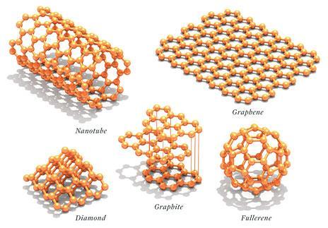
3 1996: Curl, Kroto, Smalley 1985 or 1986: fullerenes (C60, bucky balls); 2010: Geim, Novoselov : 2D graphene The allotropes of carbon: hardest natural substance, diamond one of the softest known substances, graphite. For carbon nanotubes CNT (by Ijima in 1991) and the equally important discovery of inorganic fullerene structures (by Tenne) Allotropes of carbon: a) diamond; b) graphite; c) lonsdaleite; d f) fullerenes (C 60, C 540, C 70 ); g) amorphous carbon; h) carbon nanotube. from

4 Carbon allotropes Chem. Rev. 2015, 115, Page 4
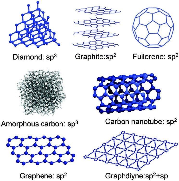
5 Carbon allotropes Page 5


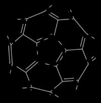
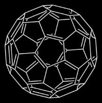
6 Fullerene: The Nobel Prize in Chemistry 1996 Robert F. Curl Jr. Sir Harold W. Kroto Richard E. Smalley The Nobel Prize in Chemistry 1996 was awarded jointly to Robert F. Curl Jr., Sir Harold W. Kroto and Richard E. Smalley "for their discovery of fullerenes" Page 6

7 Discovery of fullerenes laser evaporation of graphite Page 7


8 Fullerenes based acceptors for heterojunction organic solar cells Functionalization Page 8

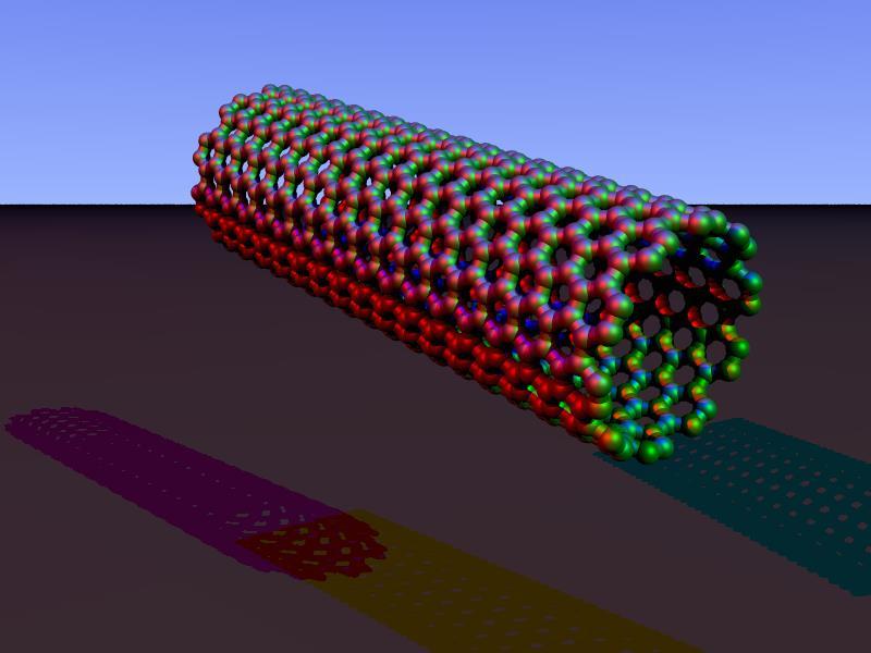
9 Page 9 Carbon nanotubes


10 MoS 2 transistors with 1-nm gate lengths - The world's smallest transistor The gate length is considered as a defining dimension of transistor, with the choice of proper materials, there is a lot more room to shrink our electronics. Science 2016, 354,


11 Graphene: The Nobel Prize in Physics 2010 Andre Geim Konstantin Novoselov for groundbreaking experiments regarding the two-dimensional material graphene Page 11

12 Graphene is a 1-atom thickness sheet of sp 2 -bonded carbon atoms that are densely packed in a honeycomb crystal lattice. Graphite consists of many graphene sheets stacked together. (


13 Zigzag carbon nanotube could be either semiconducting or metallic


14 Armchair carbon nanotube all metallic

 306, 666;")
 102, 10451. 24.01.")
15 Graphene: The Nobel Prize in Physics 2010 Highly oriented pyrolytic graphite (HOPG) Science (2004) 306, 666; Proc. Natl. Acad. Sci. (2005) 102, Page 15


16 Graphite to Graphene Exfoliation Page 16


17 D.I.Y. Graphene from graphite: top-down approach Page 17

18 Graphene The Mother Of All Graphites Graphene: a single layer of carbon packed in hexagonal lattice, with a carbon-carbon distance of nm. Graphene: a basic building block for carbon materials of all other dimensions: wrap up into 0D fullerene roll up into 1D nanotubes stacked into 3D graphite A.K. Geim & K.S. Novoselov, Nat. Mater. 2017, 6, Page 18

19 Synthesis of Graphene Page 19


20 Chemical synthesis of Graphene: Hummers method Most widely used for producing graphene by oxidizing graphite to GO by using suitable oxidizing agents. GO is then reduced to produce graphene Page 20
 of")


21 Chemical vapor deposition (CVD) of Graphene Cu or Ni foil Science 2009;324, 1312; Nature 2009, 457, Page 21

22 Page 22 Science 2009;324, 1312; Nature 2009, 457, 706.

23 Page 23 Science 2009;324, 1312; Nature 2009, 457, 706.


24 CVD of Graphene foam Nature Materials 2011, 10, Page 24


25 Graphene foam via CVD A mm 2 free-standing graphene foam Nature Materials 2011, 10, Page 25
")
 chemical removal of")

26 CVD Growth of Graphene with Ni Nanowires Formation of graphene tubular structure: (a) Ni nanowire; (b) graphene grown on Ni nanowire template; (c) chemical removal of Ni nanowire. 2 layers 3 layers 5 layers 10 layers Nano Lett. 2010, 10, Page 26


27 Synthesis of Graphene 250 ºC 1350 ºC Exfoliation of Graphite into Graphene ACS Nano, 2013, 7, High-temperature carbonization Nature Commun. 2013, 4, Page 27


28 Synthesis of Graphene: seconds timescale water electrolytic oxidation Nature Communications 2018, 9, Page 28


29 Synthesis of Graphene Science 2008, 319, Nature 2009, 458, Page 29
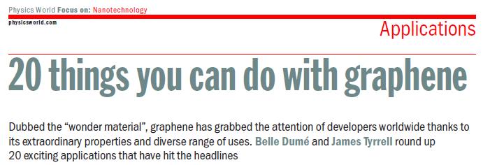
30 PECVD Growth of Vertically Oriented Graphene Carbon sources: C2H2 or CH4 Plasma gas: H2 or Ar Page 30


31 PECVD Growth of Vertically Oriented Graphene Butter Inductively Coupled Plasma Chemical Vapour Deposition (ICP CVD) Ni foam was pasted with butter prior to be loaded in reactor. A gas mixture of Ar and H 2 was fed into the system for growing VG. The power of RF plasma was at 1000 W and the growth lasted for 9 min. Adv. Energy Mater. 2013, 3, Page 31

32 Comparison of different methods for graphene mass-production Nature, 2012, 490, Page 32
33 Basic properties of Graphene Graphene's unique electronic structure enables this extraordinary material to break many records of strength, electricity and heat conduction. Density of graphene: 0.77 mg m -2 Almost optical transparent: absorbs only 2.3% of light intensity, independent of the wavelength in optical domain. Young s modulus of 1 Tera-Pascal and intrinsic strength of 130 Giga- Pascal, more than 100 times stronger than the strongest steel. RT electron mobility: μ = 200,000 cm 2 V 1 s 1. Very high thermal conductivity: ~ 3000 W m K 1, 10 times better than copper Page 33

34 Basic properties of Graphene Graphene's unique electronic structure enables this extraordinary material to break many records of strength, electricity and heat conduction Page 34

35 Energy band structure of graphene The valence band (lower band) and conduction band (upper band) of graphene touch at six points (Brillouin zone corners), thus making graphene a zero-band-gap semiconductor. More details: The electronic properties of graphene, A. H. Castro Neto, F. Guinea, N. M. R. Peres, K. S. Novoselov, and A. K. Geim, Rev. Mod. Phys. 2009, 81, Page 35

36 Graphene: zero-band-gap semiconductor Because of its symmetrical structure its atoms scatter electrons in such a way that they cancel each other out, graphene has no electronic band gap, which is the key semiconductoring property controlling the operations of transistors, lasers, and other solid-state devices Page 36

37 Widely tunable bandgap in bilayer graphene Graphene lacks a band gap because of its symmetrical structure its atoms scatter electrons in such a way that they cancel each other out. The introduction of an electric field perpendicular to the layers creates an asymmetry, which generates a band gap. Though small, the gap is tunable, creating possibilities for new devices. Nature Nanotechnology 5, 32 (2009); Nature 459, 820 (2009) Page 37

38 Chemical doping for band gap tuning in graphene The band structure near the Dirac point of bilayer epitaxial graphene grown on the surface of SiC can be easily tuned by potassium doping. Science 2006, 313, J. Mater. Chem., 2011, 21, Page 38

39 A platform to study graphene's electronic properties Device to detect graphene's electronic properties: graphene sandwiched in 2 layers of insulating BN. By tuning voltages applied on graphite and Si, the changes in conductance of graphene can be measured, which reflects its electronic properties. Nano Lett. 2017, 17, Page 39

40 Electrons of graphene represented by Dirac cone (2 cones like a sandglass), with a small point in between (Dirac Point). The differences in the electronic structures are shown as filling the sandglass by an electron liquid. Applying negative voltage on Si & graphite is equivalent to drinking, and positive voltage to filling the glass with more electron liquid. The Fermi level is the maximum level where you can find electrons Page 40

41 Page 41 Applications of graphene
42 1.Create rugged sensors 2.Sequence DNA 3.Re-imagine aircraft design 4.Detect concealed weapons 5.Build better electronics 6.Ramp up the performance of supercapacitors and batteries 7.Design new types of batteries 8.Kill E. coli bacterio 9.Print electronic devices 10.Soak up arsenic Page 42
43 11. Improve electron sources 12. Make high-performance modulators 13. Store hydrogen 14. Remove water from a mixture 15. Remove water from a mixture 16. Remove unwanted heat from electronics 17. Form transparent electrodes for displays 18. Make rare-element-free magnets 19. Store data 20. Harness energy from the Sun Page 43

44 Page 44 Nature Reviews, 2016, 1, 16033

45 Page 45 Nature Reviews, 2016, 1, 16033

46 Graphene transistor with new operating principle Graphene in a switching transistor: electric current can t be sufficiently interrupted (no band gap). A new operating principle performing switching operation with a small band gap is required: 2 top gates are placed on graphene (irradiated via He ion beam to introduce crystalline defects. Gate biases applied to 2 top gates, allowing carrier densities in top-gated graphene regions be effectively controlled. Its transistor polarity be electrically controlled and inverted (new) Page 46

47 Graphene for energy conversion and storage Nanoscale, 2013, 5, Page 47

48 12 new features of energy-storage devices by graphene Nature Reviews, 2016, 1, Page 48

49 12 new features of energy-storage devices by graphene Nature Reviews, 2016, 1, Page 49
. 24.")
50 Graphene as electrode materials for supercapacitors Graphene as electrode materials for supercapacitors: energy storage mechanism is: charges are electrochemically stored through the adsorption-desorption of electrolyte ions on the surface of graphene, socalled electric double-layer capacitors (EDLC) Page 50

51 Graphene-based supercapacitor: hummers method TEM SEM High-performance supercapacitors based on graphene for efficient energy storage under extreme environmental temperatures, a wide range of temperatures from -20 ºC to 45 ºC. Vellacheri R., Al-Haddad A., Zhao H.P., Wang W.X., Wang C.L., Lei Y.*, Nano Energy, 2014, 8, Page 51

52 Page 52


53 PECVD Growth of Vertically Oriented Graphene Carbon sources: C2H2 or CH4 Plasma gas: H2 or Ar Page 53
54 Vertically Oriented Graphene for Supercapacitors Supercapacitors have a very fast response time (sub-millisecond timescale). Supercapacitors via vertically oriented graphene could be charged and discharged in less than a millisecond, This ultrafast supercapacitor could replace the large electrolytic capacitors used in today s electronics and may someday help make electronic devices smaller and lighter. Science 2010, 329, Page 54

55 Graphene-nanotube 3D architecture for dye-sensitized solar cells Science Advance 2015,1, Showed a power conversion efficiency of 6.8 % and out-performed the counterparts with an expensive Pt wire counter electrode by a factor of Page 55

56 Graphene as electrode materials for batteries Graphene is a great substrate for LIB anode and cathode materials to create highenergy-density, fast-charging and longer-lasting batteries. Although graphite is an excellent anode in LIBs, it cannot be utilized in Na + and Al 3+ batteries because these ions are too large to effectively insert into graphite, so alternative anode materials are required, such as porous graphene composites Page 56
57 Graphene in bio-applications In addition to electronics and photonics, graphene also has great potentials in bio-applications, such as drug delivery, tissue engineering, biosensors. Graphene sheets are highly hydrophobic and tend to aggregate, exhibiting a low water dispersibility, thus are not suitable for direct bio-applications. Chem. Soc. Rev., 2017, 46, Page 57
58 Graphene in bio-applications Graphene oxide (GO) can be easily synthesized by Hummers method, offers a richer surface chemistry due to the presence of the oxide groups. Reduced graphene oxide (rgo): chemically reduced GO to remove oxygen functional groups. rgo can be considered as an intermediate structure between the graphene sheet and the highly-oxidized GO. GO and rgo can be more easily handled, especially in liquids, since they generally exhibit good water dispersibility and a very rich surface chemistry, which allows a wide range of biomedical applications. Chem. Soc. Rev., 2017, 46, Page 58

59 Graphene in biomedical applications Drug delivery Chem. Soc. Rev., 2017, 46, Page 59

60 Graphene in biomedical applications Biosensors Chem. Soc. Rev., 2017, 46, Page 60


61 Roadmap: Graphene-based display & electronic devices Nature, 2012, 490, Page 61


62 Roadmap: graphene-based photonics applications Page 62
63 The era of carbon allotropes since 2016 Nature Materials, 2013, 9, Page 63
64 Thank you!
Nanostrukturphysik (Nanostructure Physics)
") Nanostrukturphysik (Nanostructure Physics) Prof. Yong Lei & Dr. Yang Xu Fachgebiet 3D-Nanostrukturierung, Institut für Physik Contact: yong.lei@tu-ilmenau.de; yang.xu@tu-ilmenau.de Office: Unterpoerlitzer
Nanostrukturphysik (Nanostructure Physics) Prof. Yong Lei & Dr. Yang Xu Fachgebiet 3D-Nanostrukturierung, Institut für Physik Contact: yong.lei@tu-ilmenau.de; yang.xu@tu-ilmenau.de Office: Unterpoerlitzer
Carbon nanomaterials. Gavin Lawes Wayne State University.
 Carbon nanomaterials Gavin Lawes Wayne State University glawes@wayne.edu Outline 1. Carbon structures 2. Carbon nanostructures 3. Potential applications for Carbon nanostructures Periodic table from bpc.edu
Nanostrukturphysik Übung 2 (Class 3&4)
") Nanostrukturphysik Übung 2 (Class 3&4) Prof. Yong Lei & Dr. Yang Xu 2017.05.03 Fachgebiet 3D-Nanostrukturierung, Institut für Physik Contact: yong.lei@tu-ilmenau.de (3748), yang.xu@tuilmenau.de (4902)
Nanostrukturphysik Übung 2 (Class 3&4) Prof. Yong Lei & Dr. Yang Xu 2017.05.03 Fachgebiet 3D-Nanostrukturierung, Institut für Physik Contact: yong.lei@tu-ilmenau.de (3748), yang.xu@tuilmenau.de (4902)
CVD growth of Graphene. SPE ACCE presentation Carter Kittrell James M. Tour group September 9 to 11, 2014
 CVD growth of Graphene SPE ACCE presentation Carter Kittrell James M. Tour group September 9 to 11, 2014 Graphene zigzag armchair History 1500: Pencil-Is it made of lead? 1789: Graphite 1987: The first
Graphene. Tianyu Ye November 30th, 2011
 Graphene Tianyu Ye November 30th, 2011 Outline What is graphene? How to make graphene? (Exfoliation, Epitaxial, CVD) Is it graphene? (Identification methods) Transport properties; Other properties; Applications;
Initial Stages of Growth of Organic Semiconductors on Graphene
 Initial Stages of Growth of Organic Semiconductors on Graphene Presented by: Manisha Chhikara Supervisor: Prof. Dr. Gvido Bratina University of Nova Gorica Outline Introduction to Graphene Fabrication
Wafer-scale fabrication of graphene
 Wafer-scale fabrication of graphene Sten Vollebregt, MSc Delft University of Technology, Delft Institute of Mircosystems and Nanotechnology Delft University of Technology Challenge the future Delft University
Carbon Nanomaterials: Nanotubes and Nanobuds and Graphene towards new products 2030
 Carbon Nanomaterials: Nanotubes and Nanobuds and Graphene towards new products 2030 Prof. Dr. Esko I. Kauppinen Helsinki University of Technology (TKK) Espoo, Finland Forecast Seminar February 13, 2009
Graphene films on silicon carbide (SiC) wafers supplied by Nitride Crystals, Inc.
 wafers supplied by Nitride Crystals, Inc.") 9702 Gayton Road, Suite 320, Richmond, VA 23238, USA Phone: +1 (804) 709-6696 info@nitride-crystals.com www.nitride-crystals.com Graphene films on silicon carbide (SiC) wafers supplied by Nitride Crystals,
9702 Gayton Road, Suite 320, Richmond, VA 23238, USA Phone: +1 (804) 709-6696 info@nitride-crystals.com www.nitride-crystals.com Graphene films on silicon carbide (SiC) wafers supplied by Nitride Crystals,
The many forms of carbon
 The many forms of carbon Carbon is not only the basis of life, it also provides an enormous variety of structures for nanotechnology. This versatility is connected to the ability of carbon to form two
Lectures Graphene and
 Lectures 15-16 Graphene and carbon nanotubes Graphene is atomically thin crystal of carbon which is stronger than steel but flexible, is transparent for light, and conducts electricity (gapless semiconductor).
Graphene and Carbon Nanotubes
 Graphene and Carbon Nanotubes 1 atom thick films of graphite atomic chicken wire Novoselov et al - Science 306, 666 (004) 100μm Geim s group at Manchester Novoselov et al - Nature 438, 197 (005) Kim-Stormer
Conference Return Seminar- NANO2014,Moscow State University,Moscow,Russia Date: th July 2014
 Conference Return Seminar- NANO2014,Moscow State University,Moscow,Russia Date:13-1818 th July 2014 An electrochemical method for the synthesis of single and few layers graphene sheets for high temperature
Overview. Carbon in all its forms. Background & Discovery Fabrication. Important properties. Summary & References. Overview of current research
 Graphene Prepared for Solid State Physics II Pr Dagotto Spring 2009 Laurene Tetard 03/23/09 Overview Carbon in all its forms Background & Discovery Fabrication Important properties Overview of current
Nanotechnology in Consumer Products
 Nanotechnology in Consumer Products June 17, 2015 October 31, 2014 The webinar will begin at 1pm Eastern Time Perform an audio check by going to Tools > Audio > Audio Setup Wizard Chat Box Chat Box Send
Carbon Structure Simulations using Crystal Viewer Tool
 Carbon Structure Simulations using Crystal Viewer Tool The Crystal Viewer tool in nanohub.org can be used to build three carbon nanostructures: graphene sheets, Buckminsterfullerene, Bucky balls (C 60
Seminars in Nanosystems - I
 Seminars in Nanosystems - I Winter Semester 2011/2012 Dr. Emanuela Margapoti Emanuela.Margapoti@wsi.tum.de Dr. Gregor Koblmüller Gregor.Koblmueller@wsi.tum.de Seminar Room at ZNN 1 floor Topics of the
Nanostrukturphysik (Nanostructure Physics)
") Nanostrukturphysik (Nanostructure Physics) Prof. Yong Lei & Dr. Huaping Zhao Fachgebiet Angewandte Nanophysik, Institut für Physik Contact: yong.lei@tu-ilmenau.de; huaping.zhao@tu-ilmenau.de Office: Unterpoerlitzer
Nanostrukturphysik (Nanostructure Physics) Prof. Yong Lei & Dr. Huaping Zhao Fachgebiet Angewandte Nanophysik, Institut für Physik Contact: yong.lei@tu-ilmenau.de; huaping.zhao@tu-ilmenau.de Office: Unterpoerlitzer
Techniken der Oberflächenphysik (Techniques of Surface Physics)
") Techniken der Oberflächenphysik (Techniques of Surface Physics) Prof. Yong Lei & Dr. Yang Xu, Dr. Huaping Zhao Fachgebiet Angewante Nanophysik, Institut für Physik Contact: yong.lei@tu-ilmenau.de yang.xu@tu-ilmenau.de
Techniken der Oberflächenphysik (Techniques of Surface Physics) Prof. Yong Lei & Dr. Yang Xu, Dr. Huaping Zhao Fachgebiet Angewante Nanophysik, Institut für Physik Contact: yong.lei@tu-ilmenau.de yang.xu@tu-ilmenau.de
Graphene Fundamentals and Emergent Applications
 Graphene Fundamentals and Emergent Applications Jamie H. Warner Department of Materials University of Oxford Oxford, UK Franziska Schaffel Department of Materials University of Oxford Oxford, UK Alicja
Nanostrukturphysik. Prof. Yong Lei & Dr. Yang Xu Fachgebiet 3D-Nanostrukturierung, Institut für Physik
 Nanostrukturphysik Prof. Yong Lei & Dr. Yang Xu Fachgebiet 3D-Nanostrukturierung, Institut für Physik Contact: yong.lei@tu-ilmenau.de (3748), yang.xu@tuilmenau.de (4902) Office: Gebäude V202, Unterpörlitzer
Halbleiter. Prof. Yong Lei. Prof. Thomas Hannappel.
 Halbleiter Prof. Yong Lei Prof. Thomas Hannappel yong.lei@tu-ilemnau.de thomas.hannappel@tu-ilmenau.de Important Events in Semiconductors History 1833 Michael Faraday discovered temperature-dependent conductivity
Chapter 12: Structures & Properties of Ceramics
 Chapter 12: Structures & Properties of Ceramics ISSUES TO ADDRESS... How do the crystal structures of ceramic materials differ from those for metals? How do point defects in ceramics differ from those
3-month progress Report
 3-month progress Report Graphene Devices and Circuits Supervisor Dr. P.A Childs Table of Content Abstract... 1 1. Introduction... 1 1.1 Graphene gold rush... 1 1.2 Properties of graphene... 3 1.3 Semiconductor
Graphene: the Route from Touch Screens to Digital Nanoelectronics
 Graphene: the Route from Touch Screens to Digital Nanoelectronics László Péter Biró Research Institute for Technical Physics & Materials Science, Budapest, Hungary http://www.nanotechnology.hu/ Human History
STM and graphene. W. W. Larry Pai ( 白偉武 ) Center for condensed matter sciences, National Taiwan University NTHU, 2013/05/23
 Center for condensed matter sciences, National Taiwan University NTHU, 2013/05/23") STM and graphene W. W. Larry Pai ( 白偉武 ) Center for condensed matter sciences, National Taiwan University NTHU, 2013/05/23 Why graphene is important: It is a new form of material (two dimensional, single
STM and graphene W. W. Larry Pai ( 白偉武 ) Center for condensed matter sciences, National Taiwan University NTHU, 2013/05/23 Why graphene is important: It is a new form of material (two dimensional, single
Carbon Nanotubes. Andrea Goldoni. Elettra- Sincrotrone Trieste S.C.p.A., s.s. 14 Km 163,5 in Area Science Park, Trieste, Italy
 Carbon Nanotubes Andrea Goldoni Elettra- Sincrotrone Trieste S.C.p.A., s.s. 14 Km 163,5 in Area Science Park, 34012 Trieste, Italy Up to 1985 the only two allotropic form of carbon were known: graphite
Chemistry 1000 Lecture 22: Group 14 and Boron. Marc R. Roussel
 Chemistry 1000 Lecture 22: Group 14 and Boron Marc R. Roussel Group 14 In this group again, we see a full range of nonmetallic to metallic behavior: C is a nonmetal. Si and Ge are metalloids. Sn and Pb
In today s lecture, we will cover:
 In today s lecture, we will cover: Metal and Metal oxide Nanoparticles Semiconductor Nanocrystals Carbon Nanotubes 1 Week 2: Nanoparticles Goals for this section Develop an understanding of the physical
Chemistry 1000 Lecture 24: Group 14 and Boron
 Chemistry 1000 Lecture 24: Group 14 and Boron Marc R. Roussel November 2, 2018 Marc R. Roussel Group 14 and Boron November 2, 2018 1 / 17 Group 14 In this group again, we see a full range of nonmetallic
Introduction to Nanotechnology Chapter 5 Carbon Nanostructures Lecture 1
 Introduction to Nanotechnology Chapter 5 Carbon Nanostructures Lecture 1 ChiiDong Chen Institute of Physics, Academia Sinica chiidong@phys.sinica.edu.tw 02 27896766 Section 5.2.1 Nature of the Carbon Bond
GRAPHENE NANORIBBONS Nahid Shayesteh,
 USC Department of Physics Graduate Seminar 1 GRAPHENE NANORIBBONS Nahid Shayesteh, Outlines 2 Carbon based material Discovery and innovation of graphen Graphene nanoribbons structure Application of Graphene
Graphene FETs EE439 FINAL PROJECT. Yiwen Meng Su Ai
 Graphene FETs EE439 FINAL PROJECT Yiwen Meng Su Ai Introduction What is Graphene? An atomic-scale honeycomb lattice made of carbon atoms Before 2004, Hypothetical Carbon Structure Until 2004, physicists
Techniken der Oberflächenphysik (Technique of Surface Physics)
") Techniken der Oberflächenphysik (Technique of Surface Physics) Yong Lei & Fabian Grote Fachgebiet 3D-Nanostrukturierung, Institut für Physik Contact: yong.lei@tu-ilmenau.de; fabian.grote@tu-ilmenau.de
Techniken der Oberflächenphysik (Technique of Surface Physics) Yong Lei & Fabian Grote Fachgebiet 3D-Nanostrukturierung, Institut für Physik Contact: yong.lei@tu-ilmenau.de; fabian.grote@tu-ilmenau.de
e - Galvanic Cell 1. Voltage Sources 1.1 Polymer Electrolyte Membrane (PEM) Fuel Cell
 Fuel Cell") Galvanic cells convert different forms of energy (chemical fuel, sunlight, mechanical pressure, etc.) into electrical energy and heat. In this lecture, we are interested in some examples of galvanic cells.
Galvanic cells convert different forms of energy (chemical fuel, sunlight, mechanical pressure, etc.) into electrical energy and heat. In this lecture, we are interested in some examples of galvanic cells.
Supplementary Figure S1. AFM images of GraNRs grown with standard growth process. Each of these pictures show GraNRs prepared independently,
 Supplementary Figure S1. AFM images of GraNRs grown with standard growth process. Each of these pictures show GraNRs prepared independently, suggesting that the results is reproducible. Supplementary Figure
Organic Electronic Devices
 Organic Electronic Devices Week 5: Organic Light-Emitting Devices and Emerging Technologies Lecture 5.5: Course Review and Summary Bryan W. Boudouris Chemical Engineering Purdue University 1 Understanding
Plastic Electronics. Joaquim Puigdollers.
 Plastic Electronics Joaquim Puigdollers Joaquim.puigdollers@upc.edu Nobel Prize Chemistry 2000 Origins Technological Interest First products.. MONOCROMATIC PHILIPS Today Future Technological interest Low
Nanostrukturphysik (Nanostructure Physics)
") Nanostrukturphysik (Nanostructure Physics) Prof. Yong Lei & Dr. Yang Xu Fachgebiet 3D-Nanostrukturierung, Institut für Physik Contact: yong.lei@tu-ilmenau.de; yang.xu@tu-ilmenau.de Office: Unterpoerlitzer
Nanostrukturphysik (Nanostructure Physics) Prof. Yong Lei & Dr. Yang Xu Fachgebiet 3D-Nanostrukturierung, Institut für Physik Contact: yong.lei@tu-ilmenau.de; yang.xu@tu-ilmenau.de Office: Unterpoerlitzer
Carbon nanotubes and Graphene
 16 October, 2008 Solid State Physics Seminar Main points 1 History and discovery of Graphene and Carbon nanotubes 2 Tight-binding approximation Dynamics of electrons near the Dirac-points 3 Properties
Ali Ahmadpour. Fullerenes. Ali Ahmadpour. Department of Chemical Engineering Faculty of Engineering Ferdowsi University of Mashhad
 Ali Ahmadpour Fullerenes Ali Ahmadpour Department of Chemical Engineering Faculty of Engineering Ferdowsi University of Mashhad 2014 World of Carbon Materials 2 Fullerenes 1985 Robert F. Curl Jr. Richard
Energy Storage. Light-emitting. Nano-Carbons. H 2 Energy. CNT synthesis. Graphene synthesis Top-down. Solar H 2 generation
 Nano-Carbon battery Graphene synthesis Top-down CNT synthesis CVD reactor hydrocarbon gas Catalyst CNTs Chemical Modification COO O NO 2 COO COO COO Bottom-up O O NO NO 2 2 COO COO Nano-Carbons 20 nm Light-emitting
Solutions for Assignment-8
 Solutions for Assignment-8 Q1. The process of adding impurities to a pure semiconductor is called: [1] (a) Mixing (b) Doping (c) Diffusing (d) None of the above In semiconductor production, doping intentionally
EN2912C: Future Directions in Computing Lecture 08: Overview of Near-Term Emerging Computing Technologies
 EN2912C: Future Directions in Computing Lecture 08: Overview of Near-Term Emerging Computing Technologies Prof. Sherief Reda Division of Engineering Brown University Fall 2008 1 Near-term emerging computing
Nanostrukturphysik (Nanostructure Physics)
") Nanostrukturphysik (Nanostructure Physics) Prof. Yong Lei & Dr. Yang Xu Fachgebiet 3D-Nanostrukturierung, Institut für Physik Contact: yong.lei@tu-ilmenau.de; yang.xu@tu-ilmenau.de Office: Unterpoerlitzer
Nanostrukturphysik (Nanostructure Physics) Prof. Yong Lei & Dr. Yang Xu Fachgebiet 3D-Nanostrukturierung, Institut für Physik Contact: yong.lei@tu-ilmenau.de; yang.xu@tu-ilmenau.de Office: Unterpoerlitzer
Carbon based Nanoscale Electronics
 Carbon based Nanoscale Electronics 09 02 200802 2008 ME class Outline driving force for the carbon nanomaterial electronic properties of fullerene exploration of electronic carbon nanotube gold rush of
Carbon nanotubes in a nutshell. Graphite band structure. What is a carbon nanotube? Start by considering graphite.
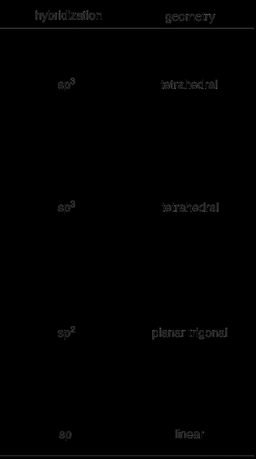
 Carbon nanotubes in a nutshell What is a carbon nanotube? Start by considering graphite. sp 2 bonded carbon. Each atom connected to 3 neighbors w/ 120 degree bond angles. Hybridized π bonding across whole
per unit cell Motif: Re at (0, 0, 0); 3O at ( 1 / 2, 0), (0, 0, 1 / 2 ) Re: 6 (octahedral coordination) O: 2 (linear coordination) ReO 6
; 3O at ( 1 / 2, 0), (0, 0, 1 / 2 ) Re: 6 (octahedral coordination) O: 2 (linear coordination) ReO 6") Lattice: Primitive Cubic 1ReO 3 per unit cell Motif: Re at (0, 0, 0); 3O at ( 1 / 2, 0, 0), (0, 1 / 2, 0), (0, 0, 1 / 2 ) Re: 6 (octahedral coordination) O: 2 (linear coordination) ReO 6 octahedra share
Lattice: Primitive Cubic 1ReO 3 per unit cell Motif: Re at (0, 0, 0); 3O at ( 1 / 2, 0, 0), (0, 1 / 2, 0), (0, 0, 1 / 2 ) Re: 6 (octahedral coordination) O: 2 (linear coordination) ReO 6 octahedra share
Grpahene Synthesis by CVD. QingkaiYu Ingram School of Engineering Texas State University at San Marcos
 Grpahene Synthesis by CVD QingkaiYu Ingram School of Engineering Texas State University at San Marcos @ Applied Nanotech Inc, July 25 th, 2011 Acknowledgement Texas State University Dr. Zhihong Liu Austin
2D MBE Activities in Sheffield. I. Farrer, J. Heffernan Electronic and Electrical Engineering The University of Sheffield
 2D MBE Activities in Sheffield I. Farrer, J. Heffernan Electronic and Electrical Engineering The University of Sheffield Outline Motivation Van der Waals crystals The Transition Metal Di-Chalcogenides
Nanostructures. Lecture 13 OUTLINE
 Nanostructures MTX9100 Nanomaterials Lecture 13 OUTLINE -What is quantum confinement? - How can zero-dimensional materials be used? -What are one dimensional structures? -Why does graphene attract so much
ELECTRONIC ENERGY DISPERSION AND STRUCTURAL PROPERTIES ON GRAPHENE AND CARBON NANOTUBES
 ELECTRONIC ENERGY DISPERSION AND STRUCTURAL PROPERTIES ON GRAPHENE AND CARBON NANOTUBES D. RACOLTA, C. ANDRONACHE, D. TODORAN, R. TODORAN Technical University of Cluj Napoca, North University Center of
Session V: Graphene. Matteo Bruna CAMBRIDGE UNIVERSITY DEPARTMENT OF ENGINEERING
 Session V: Graphene Matteo Bruna Graphene: Material in the Flatland Graphite Graphene Properties: Thinnest imaginable material Good(and tunable) electrical conductor Strongest ever measured Stiffest known
Transparent Electrode Applications
 Transparent Electrode Applications LCD Solar Cells Touch Screen Indium Tin Oxide (ITO) Zinc Oxide (ZnO) - High conductivity - High transparency - Resistant to environmental effects - Rare material (Indium)
SCIENCE & TECHNOLOGY
 Pertanika J. Sci. & Technol. 25 (S): 205-212 (2017) SCIENCE & TECHNOLOGY Journal homepage: http://www.pertanika.upm.edu.my/ Effect of Boron and Oxygen Doping to Graphene Band Structure Siti Fazlina bt
Chapter 1 Introduction
 Chapter 1 Introduction In our planet carbon forms the basis of all organic molecules which makes it the most important element of life. It is present in over 95% of the known chemical compounds overall
Semiconductor Polymer
 Semiconductor Polymer Organic Semiconductor for Flexible Electronics Introduction: An organic semiconductor is an organic compound that possesses similar properties to inorganic semiconductors with hole
Carbon Materials for Electronic, Environmental and Biomedical Application
 Carbon Materials for Electronic, Environmental and Biomedical Application Seong-Cheol Kim School of Chemical Engineering Yeungnam University Nanomaterials for Electronics & Biomedical Uses 1. Organic Nanomaterials
High-Voltage Graphene Nanowalls Supercapacitor
 High-Voltage Graphene Nanowalls Supercapacitor Graphene Task Force Project Manager Dr. Kun-Ping Huang Mechanical and Mechatronics Systems Research Laboratories Industrial Technology Research Institute
performance electrocatalytic or electrochemical devices. Nanocrystals grown on graphene could have
 Nanocrystal Growth on Graphene with Various Degrees of Oxidation Hailiang Wang, Joshua Tucker Robinson, Georgi Diankov, and Hongjie Dai * Department of Chemistry and Laboratory for Advanced Materials,
Graphene: Plane and Simple Electrical Metrology?
 Graphene: Plane and Simple Electrical Metrology? R. E. Elmquist, F. L. Hernandez-Marquez, M. Real, T. Shen, D. B. Newell, C. J. Jacob, and G. R. Jones, Jr. National Institute of Standards and Technology,
Graphene The Search For Two Dimensions. Christopher Scott Friedline Arizona State University
 Graphene The Search For Two Dimensions Christopher Scott Friedline Arizona State University What Is Graphene? Single atomic layer of graphite arranged in a honeycomb crystal lattice Consists of sp 2 -bonded
Calculating Electronic Structure of Different Carbon Nanotubes and its Affect on Band Gap
 Calculating Electronic Structure of Different Carbon Nanotubes and its Affect on Band Gap 1 Rashid Nizam, 2 S. Mahdi A. Rizvi, 3 Ameer Azam 1 Centre of Excellence in Material Science, Applied Physics AMU,
Contents. Foreword by Darrell H. Reneker
 Table of Foreword by Darrell H. Reneker Preface page xi xiii 1 Introduction 1 1.1 How big is a nanometer? 1 1.2 What is nanotechnology? 1 1.3 Historical development of nanotechnology 2 1.4 Classification
Carbon nanotubes in a nutshell
 Carbon nanotubes in a nutshell What is a carbon nanotube? Start by considering graphite. sp 2 bonded carbon. Each atom connected to 3 neighbors w/ 120 degree bond angles. Hybridized π bonding across whole
Recap (so far) Low-Dimensional & Boundary Effects
 Low-Dimensional & Boundary Effects") Recap (so far) Ohm s & Fourier s Laws Mobility & Thermal Conductivity Heat Capacity Wiedemann-Franz Relationship Size Effects and Breakdown of Classical Laws 1 Low-Dimensional & Boundary Effects Energy
Recap (so far) Ohm s & Fourier s Laws Mobility & Thermal Conductivity Heat Capacity Wiedemann-Franz Relationship Size Effects and Breakdown of Classical Laws 1 Low-Dimensional & Boundary Effects Energy
From nanophysics research labs to cell phones. Dr. András Halbritter Department of Physics associate professor
 From nanophysics research labs to cell phones Dr. András Halbritter Department of Physics associate professor Curriculum Vitae Birth: 1976. High-school graduation: 1994. Master degree: 1999. PhD: 2003.
PHYS-E0424 Nanophysics Lecture 5: Fullerenes, Carbon Nanotubes and Graphene
 PHYS-E0424 Nanophysics Lecture 5: Fullerenes, Carbon Nanotubes and Graphene PHYS-E0424 Nanophysics Lecture 5: Carbon Nanostructures Sebastiaan van Dijken 1 SEM/TEM Recently I was operating SEM for a first
SUPPLEMENTARY INFORMATION
 SUPPLEMENTARY INFORMATION Facile Synthesis of High Quality Graphene Nanoribbons Liying Jiao, Xinran Wang, Georgi Diankov, Hailiang Wang & Hongjie Dai* Supplementary Information 1. Photograph of graphene
Black phosphorus: A new bandgap tuning knob
 Black phosphorus: A new bandgap tuning knob Rafael Roldán and Andres Castellanos-Gomez Modern electronics rely on devices whose functionality can be adjusted by the end-user with an external knob. A new
Nano carbon hybrids: new materials for electronic and biomedical applications
 Nano carbon hybrids: new materials for electronic and biomedical applications Physics Department Florinda Costa & António José Fernandes Nuno Santos & Alexandre Carvalho Outline 1. Nanocarbon hybrid Materials
Carbon Nanotubes (CNTs)
") Carbon Nanotubes (s) Seminar: Quantendynamik in mesoskopischen Systemen Florian Figge Fakultät für Physik Albert-Ludwigs-Universität Freiburg July 7th, 2010 F. Figge (University of Freiburg) Carbon Nanotubes
Carbon Nanotubes (s) Seminar: Quantendynamik in mesoskopischen Systemen Florian Figge Fakultät für Physik Albert-Ludwigs-Universität Freiburg July 7th, 2010 F. Figge (University of Freiburg) Carbon Nanotubes
Supporting Information Available:
 Supporting Information Available: Photoresponsive and Gas Sensing Field-Effect Transistors based on Multilayer WS 2 Nanoflakes Nengjie Huo 1, Shengxue Yang 1, Zhongming Wei 2, Shu-Shen Li 1, Jian-Bai Xia
1. Nanotechnology & nanomaterials -- Functional nanomaterials enabled by nanotechnologies.
 Novel Nano-Engineered Semiconductors for Possible Photon Sources and Detectors NAI-CHANG YEH Department of Physics, California Institute of Technology 1. Nanotechnology & nanomaterials -- Functional nanomaterials
Classification of Solids
 Classification of Solids Classification by conductivity, which is related to the band structure: (Filled bands are shown dark; D(E) = Density of states) Class Electron Density Density of States D(E) Examples
554 Chapter 10 Liquids and Solids
 554 Chapter 10 Liquids and Solids above 7376 kpa, CO 2 is a supercritical fluid, with properties of both gas and liquid. Like a gas, it penetrates deep into the coffee beans; like a liquid, it effectively
Transient Photocurrent Measurements of Graphene Related Materials
 Transient Photocurrent Measurements of Graphene Related Materials P. Srinivasa Rao Mentor: Prof. dr. Gvido Bratina Laboratory of Organic Matter Physics University of Nova Gorica 1 Contents: 1. Electrical
Marriage of Graphene and Cellulose for Reinforced Composite Preparation Zaiton Abdul Majid, Wan Hazman Danial and Mohd Bakri Bakar
 Graphene Malaysia 2016 8-9 th Nov 2016 Marriage of Graphene and Cellulose for Reinforced Composite Preparation Zaiton Abdul Majid, Wan Hazman Danial and Mohd Bakri Bakar Graphene Synthesis Fundamental
Imaging Carbon materials with correlative Raman-SEM microscopy. Introduction. Raman, SEM and FIB within one chamber. Diamond.
 Imaging Carbon materials with correlative Raman-SEM microscopy Application Example Carbon materials are widely used in many industries for their exceptional properties. Electric conductance, light weight,
Halbleiter Prof. Yong Lei Prof. Thomas Hannappel
 Halbleiter Prof. Yong Lei Prof. Thomas Hannappel yong.lei@tu-ilmenau.de thomas.hannappel@tu-ilmenau.de http://www.tu-ilmenau.de/nanostruk/ Organic Semiconductors & Organic Electronics Organic semiconductors
Carbon Engineering Nanocarbon Structures
 Carbon Engineering Nanocarbon Structures Diamond Fullerenes Carbon nanotubes (CNT) multiwalled (MNT) Diamond Like Carbon (DLC) Graphene Nanospheres Allotropes of Carbon Crystalline Diamond Graphite Carbon
Nanocarbon Technology for Development of Innovative Devices
 Nanocarbon Technology for Development of Innovative Devices Shintaro Sato Daiyu Kondo Shinichi Hirose Junichi Yamaguchi Graphene, a one-atom-thick honeycomb lattice made of carbon, and a carbon nanotube,
Why are we so excited about carbon nanostructures? Mildred Dresselhaus Massachusetts Institute of Technology Cambridge, MA
 Why are we so excited about carbon nanostructures? Mildred Dresselhaus Massachusetts Institute of Technology Cambridge, MA Conference for Undergraduate Women in Physics at Yale January 18, 2009 Why are
Introduction to Nanotechnology Chapter 5 Carbon Nanostructures Lecture 1
 Introduction to Nanotechnology Chapter 5 Carbon Nanostructures Lecture 1 ChiiDong Chen Institute of Physics, Academia Sinica chiidong@phys.sinica.edu.tw 02 27896766 Carbon contains 6 electrons: (1s) 2,
Transistori ad effetto di campo con canale in grafene (GFET) aventi risposta fotoelettrica
 aventi risposta fotoelettrica") Transistori ad effetto di campo con canale in grafene (GFET) aventi risposta fotoelettrica M. A. Giambra, E. Calandra, S. Stivala, A. Busacca DEIM Università di Palermo, via delle Scienze, Edifico 9, 90128,
Transistori ad effetto di campo con canale in grafene (GFET) aventi risposta fotoelettrica M. A. Giambra, E. Calandra, S. Stivala, A. Busacca DEIM Università di Palermo, via delle Scienze, Edifico 9, 90128,
Graphene based FETs. Raghav Gupta ( )
") 1 Graphene based FETs Raghav Gupta (10327553) Abstract The extraordinary electronic properties along with excellent optical, mechanical, thermodynamic properties have led to a lot of interest in its possible
1 Graphene based FETs Raghav Gupta (10327553) Abstract The extraordinary electronic properties along with excellent optical, mechanical, thermodynamic properties have led to a lot of interest in its possible
Introduction to Semiconductor Physics. Prof.P. Ravindran, Department of Physics, Central University of Tamil Nadu, India
 Introduction to Semiconductor Physics 1 Prof.P. Ravindran, Department of Physics, Central University of Tamil Nadu, India http://folk.uio.no/ravi/cmp2013 Review of Semiconductor Physics Semiconductor fundamentals
Graphene - most two-dimensional system imaginable
 Graphene - most two-dimensional system imaginable A suspended sheet of pure graphene a plane layer of C atoms bonded together in a honeycomb lattice is the most two-dimensional system imaginable. A.J.
The goal of this project is to enhance the power density and lowtemperature efficiency of solid oxide fuel cells (SOFC) manufactured by atomic layer
 manufactured by atomic layer") Stanford University Michael Shandalov1, Shriram Ramanathan2, Changhyun Ko2 and Paul McIntyre1 1Department of Materials Science and Engineering, Stanford University 2Division of Engineering and Applied
Stanford University Michael Shandalov1, Shriram Ramanathan2, Changhyun Ko2 and Paul McIntyre1 1Department of Materials Science and Engineering, Stanford University 2Division of Engineering and Applied
XPS Depth Profiling of Epitaxial Graphene Intercalated with FeCl 3
 XPS Depth Profiling of Epitaxial Graphene Intercalated with FeCl 3 Mahdi Ibrahim Maynard H. Jackson High School Atlanta, GA. Faculty Advisor: Dr. Kristin Shepperd Research Group: Prof. Edward Conrad School
A comparative computational study of the electronic properties of planar and buckled silicene
 A comparative computational study of the electronic properties of planar and buckled silicene Harihar Behera 1 and Gautam Mukhopadhyay 2 Indian Institute of Technology Bombay, Powai, Mumbai-400076, India
Modeling and Performance analysis of Metallic CNT Interconnects for VLSI Applications
 IOSR Journal of Electronics and Communication Engineering (IOSR-JECE) e-issn: 2278-2834, p- ISSN: 2278-8735. Volume 4, Issue 6 (Jan. - Feb. 2013), PP 32-36 Modeling and Performance analysis of Metallic
Transparent TiO 2 nanotube/nanowire arrays on TCO coated glass substrates: Synthesis and application to solar energy conversion
 Transparent TiO 2 nanotube/nanowire arrays on TCO coated glass substrates: Synthesis and application to solar energy conversion Craig A. Grimes Department of Electrical Engineering Center for Solar Nanomaterials
The World of Carbon Nanotubes
 The World of Carbon Nanotubes Carbon Nanotubes Presentation by Jan Felix Eschermann at JASS05 from March 31st to April 9th, 2005 1 Outline Introduction Physical Properties Manufacturing Techniques Applications
Electrons are shared in covalent bonds between atoms of Si. A bound electron has the lowest energy state.
 Photovoltaics Basic Steps the generation of light-generated carriers; the collection of the light-generated carriers to generate a current; the generation of a large voltage across the solar cell; and
Nanomaterials and their Optical Applications
 Nanomaterials and their Optical Applications Winter Semester 2012 Lecture 06 Tentative version of November 13, 2012 Check for the definitive version after the lecture rachel.grange@uni-jena.de http://www.iap.uni-jena.de/multiphoton
Carbon Nanotubes for Interconnect Applications Franz Kreupl, Andrew P. Graham, Maik Liebau, Georg S. Duesberg, Robert Seidel, Eugen Unger
 Carbon Nanotubes for Interconnect Applications Franz Kreupl, Andrew P. Graham, Maik Liebau, Georg S. Duesberg, Robert Seidel, Eugen Unger Infineon Technologies Corporate Research Munich, Germany Outline
Layered Compounds. Two-dimensional layers. Graphite. Clay Minerals. Layered Double Hydroxides (LDHs) Layered α-zirconium Phosphates and Phosphonates
 Layered α-zirconium Phosphates and Phosphonates") Layered Compounds Two-dimensional layers Graphite Clay Minerals Layered Double Hydroxides (LDHs) Layered α-zirconium Phosphates and Phosphonates Layered Manganese Oxides Layered Metal Chalcogenides Alkali
Layered Compounds Two-dimensional layers Graphite Clay Minerals Layered Double Hydroxides (LDHs) Layered α-zirconium Phosphates and Phosphonates Layered Manganese Oxides Layered Metal Chalcogenides Alkali
Supplementary Information
 Supplementary Information Supplementary Figure 1. fabrication. A schematic of the experimental setup used for graphene Supplementary Figure 2. Emission spectrum of the plasma: Negative peaks indicate an
Carbon Nanotubes in Interconnect Applications
 Carbon Nanotubes in Interconnect Applications Page 1 What are Carbon Nanotubes? What are they good for? Why are we interested in them? - Interconnects of the future? Comparison of electrical properties