1. Nanotechnology & nanomaterials -- Functional nanomaterials enabled by nanotechnologies.
|
|
|
- Julia Houston
- 5 years ago
- Views:
Transcription

 & FET s and quantum dots based on Si nano-pillars. 3.")
1 Novel Nano-Engineered Semiconductors for Possible Photon Sources and Detectors NAI-CHANG YEH Department of Physics, California Institute of Technology 1. Nanotechnology & nanomaterials -- Functional nanomaterials enabled by nanotechnologies. 2. Semiconducting nanowires -- Why semiconducting nanowires? (Physics, applications & fabrication) -- Fabrication of NWs. -- Novel properties of strained silicon nano-pillar arrays (2 ~ 5 nm diameters) & FET s and quantum dots based on Si nano-pillars. 3. Graphene nanoribbons & related nanostructures -- The rise of graphene. -- Physics of graphene. -- Novel phenomena of graphene & related structures. -- Potential applications to light emission & photodetection.
2 * In collaboration with M.L. Teague, C. R. Hughes, A.D. Beyer, A. P. Lai, T.-P. PW Wu (Caltech) Prof. A. Scherer & group members (Caltech) Prof. M.W. Bockrath & Prof. C.-N. Lau (UC Riverside) * Funding agencies National Science Foundation, Moore Foundation, and Kavli Foundation (Caltech) National Science Foundation (UC Riverside)
3 1. Nanotechnology & nanomaterials -- Functional nanomaterials enabled by nanotechnologies. 2. Semiconducting nanowires (NWs) 3. Graphene nanoribbons & other related nanostructures


 (nanowires, nanotubes) (quantum")

4 1. Nanotechnologies & Nanomaterials Nanotechnologies have enabled uniquely functionalized or structured nano-materials ( meta-materials ) for: studies of low-dimensional physics in quantum confinement; applications from A to B (astronomy, biology, beyond CMOS, etc.) Reduced dimensionalities: Two-dimensional One-dimensional Zero-dimensional (graphene, 2DEG) (nanowires, nanotubes) (quantum dots, nanocrystals) op/images/graphene_xyz.jpg V. G. Dubrovskiia et al., Semiconductors 43, (2009) L. Kouwenhoven et al., Phys. World (2001)
5 1. Nanotechnology & nanomaterials 2. Semiconducting nanowires -- Why semiconducting nanowires? (Physics, applications & fabrication) -- Fabrication of NWs. -- Novel properties of strained silicon nano-pillar arrays (2 ~ 5 nm diameters) & FET s and quantum dots based on silicon nano-pillars. 3. Graphene nanoribbons & related nanostructures
 have been demonstrated to be highly versatile optoelectronic components for a wide variety of applications, including: * polarization-sensitive photodetectors & arrays")
6 2. Semiconducting Nanowires (NWs) Why semiconducting NWs? Semiconducting nanowires (NWs) have been demonstrated to be highly versatile optoelectronic components for a wide variety of applications, including: * polarization-sensitive photodetectors & arrays with sub-wavelength resolution; * polarization-sensitive nano-apd (with gains up to 10 5 ); * optical modulators & nano-waveguides; * nano-leds and nano-lasers ; * solar cells, biomedical sensors, etc. Bulk Ge 10 nm 25 nm 110 nm Germanium nanowire L. Y. Cao et al. (2009)
7 Polarization-sensitive & spatially resolved nano-apds p-type Si-NW & n-type CdS-NW p-si n-cds 10 m Gain up to 10 5 V b = 10V = 488 nm No cross talk Spatial resolution better than 250nm Polarization -sensitive Hayden et al. Nature Mat. 5, 352 (2006)


8 2.2. Fabrication of NWs Mechanism of the growth vapor-liquid-crystal: id l V. G. Dubrovskiia etal., Semiconductors 43, (2009) An ensemble of GaAs-NWs grown by MBE An individual GaAs-NW
9 Formation of NWs by selective epitaxy on treated surfaces w/o a catalyst: V. G. Dubrovskiia et al., Semiconductors 43, (2009) GaAs-NWs GaAs-NWs grown on the grown on the GaAs (111) GaAs (111) surface for surface for d 0 = 200 nm d 0 = 50 nm Other growth mechanisms such as self-assembly, etc.


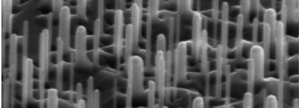
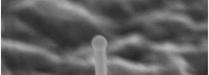
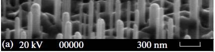
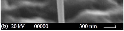
10 2.3. Strained silicon nano-pillars (Axel Scherer s group) When small silicon pillars are oxidized, the silicon lattice expands by approximately 40%, which leaves the adjacent un-oxidized silicon under tremendous tensile strain. In nanowires, this strain can increase to the point where the silicon oxidation process is selflimited, leaving stable 2 ~ 10 nm wide tensile-strained silicon cores within a silicon dioxide shells. The nano-pillar diameter is controlled by the oxidization temperature. t
11 Atomically resolved imaging & spectroscopy using scanning tunneling microscopy (STM) STM operation is based on: 1) Quantum tunneling of electrons -- Tunneling current (I) depends strongly on the surface work function ( ), the separation (s) and the biased voltage (V) between the tip & sample. 2) Piezoelectric control -- Enables atomic scale resolution for surface topography and lateral scanning capabilities. i Two primary modes of operation: 1) Three-dimensional imaging -- Under feedback control, the constant current map. 2) Spectroscopy -- Fixed location differential conductance (di/dv)-vs.-v map, under constant. Tunneling current (I) Two mode of operation: 1) imaging, 2) spectroscopy. NbSe 2 Electrons tunnel across vacuum


12 Strain-enhanced energy gap in silicon nano-pillars Spatially resolved spectroscopy of HF-etched silicon nano-pillars Surface topography from STM after HF chemical etching 3 ev 250 nm The energy gap increases from ~ 1.11 ev for crystalline silicon to ~ 3.o ev for the strained silicon nano-pillars. (Our preliminary STM results) Further quantum confinement is expected for a finite magnetic field parallel to the silicon nano-pillars, because the diameter of the nanopillars is typically smaller than the cyclotron orbit.
13 Making a transistor out of a strained silicon nano-pillar: (Courtesy of Axel Scherer)


14 Similar transistor structures have been demonstrated in InAs nanowires with larger diameters and separations: V G Dubrovskiia etal V. G. Dubrovskiia et al., Semiconductors 43, (2009)
15 1. Nanotechnology & nanomaterials 2. Semiconducting nanowires 3. Graphene nanoribbons & related nanostructures t -- The rise of graphene. -- Physics of graphene. -- Novel phenomena of graphene and related structures. -- Potential applications to light emission & photodetection.


16 3. Graphene Nanoribbons & Related Nanostructures The Rise of Graphene Carbon structures in different dimensions: 0D 1D 2D 3D Graphene consists of carbon atoms in honeycomb lattice. Unique Dispersion Relations: massless Dirac Fermions. First experimental isolation by Geim s group in [Novoselov et al, Science (2005).] Two sublattices in the honeycomb lattice: (Courtesy of M.W. Bockrath) Energy Single layer Bilayer k


 3 1 4cos cos")
.")
17 3.2. Physics of graphene Electronic bandstructures bandstructures of graphene: Tight binding approximation, assuming a perfectly ordered infinite system, 3 covalently bonded sp 2 and 1 2p z conduction electrons. The resulting E 2D (k) band structure is Near the Dirac points K & K' 3ka ka y ka x 2 y E 2 D( kx, ky) 3 1 4cos cos 4cos ( ev) vf k Images: Ph.D. thesis of Jinseong Heo, Caltech (2008). Image from: op/images/graphene_xyz.jpg
18 Graphene bipolar field effect transistors (FETs) Hole doped Electron doped Dirac point EF E F E F The unique bandstructures of graphene suppress carrier backscattering, leading to extremely high mobility. Conductivity ( ) increases linearly with charge density (n): V g n Extremely high mobility: ~ 15,000 cm 2 /Vs in as-prepared, non-optimized samples, compared to ~ 2,000 cm 2 /Vs for silicon. Conductivity remains finite at Dirac point min (Novoselov et al, Nature, 2005, Zhang et al, Nature 2005, Miao et al, Science 2007, Kim group, Fuhrer group.)
19 Demonstrated t applications: Applications of Graphene Transparent electrodes for solar cells, LCD, etc. Robust, non-volatile, atomic switches. Chemical and biological sensors based on graphene. Electronics, Spintronics, and Valley-tronics. Post silicon electronic materials: With advantages of carbon nanotubes. high thermal conductivity (~5000 W/mK) high current density (~ ma/ m width) high mobility (~20,000 cm 2 /Vs in as-prepared samples, 300,000 if suspended) supports ballistic transport over large distances 2D compatible with lithographic techniques. Potential for large scale synthesis.

 Graphene is a semi-metal, or zero-gap semiconductor.")

20 Challenges & Current Research DIrections Large-scale & high-quality production MBE or CVD growth. Device and bandgap engineering graphane (i.e. hydrogenated graphene) nanoribbons atomic switches local strain Graphane (0 ~ 3.5 ev) Graphene is a semi-metal, or zero-gap semiconductor. How does one engineer an energy gap in graphenebased systems? Novel devices ballistic transistors supercollimators & electronic lensing Schottky diodes & light emitting diodes photodectors Graphene nanoribbon ( 0 ~ 200 mev)
21 3.3. Novel properties of graphene & related structures Energy gap engineering of graphene nanoribbons (GNR): * Band gap induced by quantum confinement. * GNR field effect transistors (FETs). * Lithographically or chemically defined nanoribbons. E g 0.2 ev * W W nm GNR-FET M. Y. Han et al. (2007) * On/Off ratio ~ * Mobility ~ 200 cm 2 /Vs.
22 Strain-induced induced modifications to the electronic properties of graphene: 1. Mechanically exfoliated graphene on SiO2. 2. CVD-grown graphene on Cu.


23 STM calibration on graphite We tested on graphite to calibrate STM and verify tip quality. STM topography scan over graphite manifests the A-B- A-B stacking of graphene hexagon sheets, known as the Bernal stacking.


 correlated")
24 STM studies of graphene on SiO 2 STM topographic image of graphene reveals a distorted honeycomb lattice, showing surface corrugations (~ 0.7 nm z-axis modulations over ~ 20 nm distance) correlated with the underlying SiO 2 substrate.


25 STM studies of graphene on SiO 2 Fourier transform of the topographic image of graphene reveals a strained-induced distorted reciprocal lattice. Local electronic properties are also modified by the strain fields.


 = u x (x,y)/ x")
 = S xy (x,y) = [ u x")
![(x,y)/ y + u y (x,y)/ x]/2 V B](/docs-images/93/114197724/images/26-8.jpg "= 80 mev V B = 240 mev")
26 Strained-induced induced conductance modulations Constant-V B conductance maps at small V B values correlate with overall surface corrugation and the resulting strain fields. Topography V B = 0 Maps of strain tensor components: S 00 S xx S xx (x,y) = u x (x,y)/ x S yy (x,y) = u y (x,y)/ y S xy (x,y) = S xy (x,y) = [ u x (x,y)/ y + u y (x,y)/ x]/2 V B = 80 mev V B = 240 mev Displacement field: u(x,y) = [u x (x,y) e x + u y (x,y) e y ] S xy S yy
 T = 0 Theoretical curve with ph = 24 mev References: Y. Zhang et al, Nature ph varies Phys. 4 (2008). from 21 mev T.O.")
27 Strain-induced induced modifications in the out-of of-plane phonon- assisted tunneling gaps & conductance T = 0 Theoretical curve with ph = 42 mev This work: M.L. Teague et al, Nano Letters 9, 2542 (2009) T = 0 Theoretical curve with ph = 24 mev References: Y. Zhang et al, Nature ph varies Phys. 4 (2008). from 21 mev T.O. Wehling et al, to 44 mev. PRL 101 (2008).
28 The out-of-plane phonon frequencies increase with increasing strain, suggesting coupling of -electrons to the underlying phonons of the dielectric SiO 2. N.-C. Yeh et al, preprint, (2010).
29 Strain-induced induced structural & conductance modifications in large-scale CVD grown graphene on copper CVD growth of graphene on copper foils at ~ 1000 C under hydrogen gas with CH 4 partial pressure. Large differences in the thermal contraction coefficients of graphene and copper lead to ripple structures. [ N.-C. Yeh et al, (2010) ]

 t Fouriertransformed")
.")

30 Modifications to electronic properties due to structural changes Topography (distorted structure) t Fouriertransformed structure t N.-C. Yeh et al, (2010). Conductance spectra of representative regions a b Conductance spectra along the dashed line in the upper left figure.


31 3.4. Potential applications to light emission & photodetection Graphene nanoribbons: semiconducting energy gaps may be engineered by the controlling the width, from 0 ~ 200 mev. Graphane: semiconducting energy gaps may be engineered by controlling the hydrogen coverage, from 0 ~ 3.5 ev. Device concept Light emission The light emitting process may be reversed for the detection of photocurrents. t (or graphene nanoribbons) Future work: measurements of the I-V characteristics & photocurrents.


32 Summary Novel nanostructures such as strained silicon nano-pillars, semiconducting nanowires and graphene-based nano-devices may be interesting candidates for new types of ultra-high-density ultra-compact sensitive photodetectors, possibly even single-photon-counting detectors. 10 m
Carbon based Nanoscale Electronics
 Carbon based Nanoscale Electronics 09 02 200802 2008 ME class Outline driving force for the carbon nanomaterial electronic properties of fullerene exploration of electronic carbon nanotube gold rush of
Graphene and Carbon Nanotubes
 Graphene and Carbon Nanotubes 1 atom thick films of graphite atomic chicken wire Novoselov et al - Science 306, 666 (004) 100μm Geim s group at Manchester Novoselov et al - Nature 438, 197 (005) Kim-Stormer
Graphene. Tianyu Ye November 30th, 2011
 Graphene Tianyu Ye November 30th, 2011 Outline What is graphene? How to make graphene? (Exfoliation, Epitaxial, CVD) Is it graphene? (Identification methods) Transport properties; Other properties; Applications;
Surface atoms/molecules of a material act as an interface to its surrounding environment;
 1 Chapter 1 Thesis Overview Surface atoms/molecules of a material act as an interface to its surrounding environment; their properties are often complicated by external adsorbates/species on the surface
Overview. Carbon in all its forms. Background & Discovery Fabrication. Important properties. Summary & References. Overview of current research
 Graphene Prepared for Solid State Physics II Pr Dagotto Spring 2009 Laurene Tetard 03/23/09 Overview Carbon in all its forms Background & Discovery Fabrication Important properties Overview of current
Lectures Graphene and
 Lectures 15-16 Graphene and carbon nanotubes Graphene is atomically thin crystal of carbon which is stronger than steel but flexible, is transparent for light, and conducts electricity (gapless semiconductor).
Seminars in Nanosystems - I
 Seminars in Nanosystems - I Winter Semester 2011/2012 Dr. Emanuela Margapoti Emanuela.Margapoti@wsi.tum.de Dr. Gregor Koblmüller Gregor.Koblmueller@wsi.tum.de Seminar Room at ZNN 1 floor Topics of the
Nanostructures. Lecture 13 OUTLINE
 Nanostructures MTX9100 Nanomaterials Lecture 13 OUTLINE -What is quantum confinement? - How can zero-dimensional materials be used? -What are one dimensional structures? -Why does graphene attract so much
Optimizing Graphene Morphology on SiC(0001)
") Optimizing Graphene Morphology on SiC(0001) James B. Hannon Rudolf M. Tromp Graphene sheets Graphene sheets can be formed into 0D,1D, 2D, and 3D structures Chemically inert Intrinsically high carrier mobility
Optimizing Graphene Morphology on SiC(0001) James B. Hannon Rudolf M. Tromp Graphene sheets Graphene sheets can be formed into 0D,1D, 2D, and 3D structures Chemically inert Intrinsically high carrier mobility
NiCl2 Solution concentration. Etching Duration. Aspect ratio. Experiment Atmosphere Temperature. Length(µm) Width (nm) Ar:H2=9:1, 150Pa
 Width (nm) Ar:H2=9:1, 150Pa") Experiment Atmosphere Temperature #1 # 2 # 3 # 4 # 5 # 6 # 7 # 8 # 9 # 10 Ar:H2=9:1, 150Pa Ar:H2=9:1, 150Pa Ar:H2=9:1, 150Pa Ar:H2=9:1, 150Pa Ar:H2=9:1, 150Pa Ar:H2=9:1, 150Pa Ar:H2=9:1, 150Pa Ar:H2=9:1,
Experiment Atmosphere Temperature #1 # 2 # 3 # 4 # 5 # 6 # 7 # 8 # 9 # 10 Ar:H2=9:1, 150Pa Ar:H2=9:1, 150Pa Ar:H2=9:1, 150Pa Ar:H2=9:1, 150Pa Ar:H2=9:1, 150Pa Ar:H2=9:1, 150Pa Ar:H2=9:1, 150Pa Ar:H2=9:1,
Graphene Fundamentals and Emergent Applications
 Graphene Fundamentals and Emergent Applications Jamie H. Warner Department of Materials University of Oxford Oxford, UK Franziska Schaffel Department of Materials University of Oxford Oxford, UK Alicja
3-month progress Report
 3-month progress Report Graphene Devices and Circuits Supervisor Dr. P.A Childs Table of Content Abstract... 1 1. Introduction... 1 1.1 Graphene gold rush... 1 1.2 Properties of graphene... 3 1.3 Semiconductor
GRAPHENE NANORIBBONS Nahid Shayesteh,
 USC Department of Physics Graduate Seminar 1 GRAPHENE NANORIBBONS Nahid Shayesteh, Outlines 2 Carbon based material Discovery and innovation of graphen Graphene nanoribbons structure Application of Graphene
Wafer-scale fabrication of graphene
 Wafer-scale fabrication of graphene Sten Vollebregt, MSc Delft University of Technology, Delft Institute of Mircosystems and Nanotechnology Delft University of Technology Challenge the future Delft University
Minimal Update of Solid State Physics
 Minimal Update of Solid State Physics It is expected that participants are acquainted with basics of solid state physics. Therefore here we will refresh only those aspects, which are absolutely necessary
Graphene films on silicon carbide (SiC) wafers supplied by Nitride Crystals, Inc.
 wafers supplied by Nitride Crystals, Inc.") 9702 Gayton Road, Suite 320, Richmond, VA 23238, USA Phone: +1 (804) 709-6696 info@nitride-crystals.com www.nitride-crystals.com Graphene films on silicon carbide (SiC) wafers supplied by Nitride Crystals,
9702 Gayton Road, Suite 320, Richmond, VA 23238, USA Phone: +1 (804) 709-6696 info@nitride-crystals.com www.nitride-crystals.com Graphene films on silicon carbide (SiC) wafers supplied by Nitride Crystals,
Graphite, graphene and relativistic electrons
 Graphite, graphene and relativistic electrons Introduction Physics of E. graphene Y. Andrei Experiments Rutgers University Transport electric field effect Quantum Hall Effect chiral fermions STM Dirac
Black phosphorus: A new bandgap tuning knob
 Black phosphorus: A new bandgap tuning knob Rafael Roldán and Andres Castellanos-Gomez Modern electronics rely on devices whose functionality can be adjusted by the end-user with an external knob. A new
Chun Ning Lau (Jeanie) Graphene Quantum Electronics: p-n Junctions and Atomic Switches
 Graphene Quantum Electronics: p-n Junctions and Atomic Switches") Chun Ning Lau (Jeanie) Graphene Quantum Electronics: p-n Junctions and Atomic Switches Acknowledgement Graduate Students Feng Miao Wenzhong Bao Discussion With Shan-Wan Tsai, Antonio Castro-Neto, Michael
Chun Ning Lau (Jeanie) Graphene Quantum Electronics: p-n Junctions and Atomic Switches Acknowledgement Graduate Students Feng Miao Wenzhong Bao Discussion With Shan-Wan Tsai, Antonio Castro-Neto, Michael
Outline. Introduction: graphene. Adsorption on graphene: - Chemisorption - Physisorption. Summary
 Outline Introduction: graphene Adsorption on graphene: - Chemisorption - Physisorption Summary 1 Electronic band structure: Electronic properties K Γ M v F = 10 6 ms -1 = c/300 massless Dirac particles!
& Dirac Fermion confinement Zahra Khatibi
 Graphene & Dirac Fermion confinement Zahra Khatibi 1 Outline: What is so special about Graphene? applications What is Graphene? Structure Transport properties Dirac fermions confinement Necessity External
Lecture 3: Heterostructures, Quasielectric Fields, and Quantum Structures
 Lecture 3: Heterostructures, Quasielectric Fields, and Quantum Structures MSE 6001, Semiconductor Materials Lectures Fall 2006 3 Semiconductor Heterostructures A semiconductor crystal made out of more
Spatially resolving density-dependent screening around a single charged atom in graphene
 Supplementary Information for Spatially resolving density-dependent screening around a single charged atom in graphene Dillon Wong, Fabiano Corsetti, Yang Wang, Victor W. Brar, Hsin-Zon Tsai, Qiong Wu,
Chapter 3 Properties of Nanostructures
 Chapter 3 Properties of Nanostructures In Chapter 2, the reduction of the extent of a solid in one or more dimensions was shown to lead to a dramatic alteration of the overall behavior of the solids. Generally,
Graphene: Plane and Simple Electrical Metrology?
 Graphene: Plane and Simple Electrical Metrology? R. E. Elmquist, F. L. Hernandez-Marquez, M. Real, T. Shen, D. B. Newell, C. J. Jacob, and G. R. Jones, Jr. National Institute of Standards and Technology,
Physics and Material Science of Semiconductor Nanostructures
 Physics and Material Science of Semiconductor Nanostructures PHYS 570P Prof. Oana Malis Email: omalis@purdue.edu Course website: http://www.physics.purdue.edu/academic_programs/courses/phys570p/ 1 Introduction
Supplementary Information
 Supplementary Information Supplementary Figure 1. fabrication. A schematic of the experimental setup used for graphene Supplementary Figure 2. Emission spectrum of the plasma: Negative peaks indicate an
From nanophysics research labs to cell phones. Dr. András Halbritter Department of Physics associate professor
 From nanophysics research labs to cell phones Dr. András Halbritter Department of Physics associate professor Curriculum Vitae Birth: 1976. High-school graduation: 1994. Master degree: 1999. PhD: 2003.
Physics and Material Science of Semiconductor Nanostructures
 Physics and Material Science of Semiconductor Nanostructures PHYS 570P Prof. Oana Malis Email: omalis@purdue.edu Course website: http://www.physics.purdue.edu/academic_programs/courses/phys570p/ 1 Course
Graphene Novel Material for Nanoelectronics
 Graphene Novel Material for Nanoelectronics Shintaro Sato Naoki Harada Daiyu Kondo Mari Ohfuchi (Manuscript received May 12, 2009) Graphene is a flat monolayer of carbon atoms with a two-dimensional honeycomb
Electroluminescence from Silicon and Germanium Nanostructures
 Electroluminescence from silicon Silicon Getnet M. and Ghoshal S.K 35 ORIGINAL ARTICLE Electroluminescence from Silicon and Germanium Nanostructures Getnet Melese* and Ghoshal S. K.** Abstract Silicon
Transversal electric field effect in multilayer graphene nanoribbon
 Transversal electric field effect in multilayer graphene nanoribbon S. Bala kumar and Jing Guo a) Department of Electrical and Computer Engineering, University of Florida, Gainesville, Florida 32608, USA
Fundamentals of Nanoelectronics: Basic Concepts
 Fundamentals of Nanoelectronics: Basic Concepts Sławomir Prucnal FWIM Page 1 Introduction Outline Electronics in nanoscale Transport Ohms law Optoelectronic properties of semiconductors Optics in nanoscale
KAVLI v F. Curved graphene revisited. María A. H. Vozmediano. Instituto de Ciencia de Materiales de Madrid CSIC
 KAVLI 2012 v F Curved graphene revisited María A. H. Vozmediano Instituto de Ciencia de Materiales de Madrid CSIC Collaborators ICMM(Graphene group) http://www.icmm.csic.es/gtg/ A. Cano E. V. Castro J.
2D MBE Activities in Sheffield. I. Farrer, J. Heffernan Electronic and Electrical Engineering The University of Sheffield
 2D MBE Activities in Sheffield I. Farrer, J. Heffernan Electronic and Electrical Engineering The University of Sheffield Outline Motivation Van der Waals crystals The Transition Metal Di-Chalcogenides
Classification of Solids
 Classification of Solids Classification by conductivity, which is related to the band structure: (Filled bands are shown dark; D(E) = Density of states) Class Electron Density Density of States D(E) Examples
Transient Photocurrent Measurements of Graphene Related Materials
 Transient Photocurrent Measurements of Graphene Related Materials P. Srinivasa Rao Mentor: Prof. dr. Gvido Bratina Laboratory of Organic Matter Physics University of Nova Gorica 1 Contents: 1. Electrical
Electric Field-Dependent Charge-Carrier Velocity in Semiconducting Carbon. Nanotubes. Yung-Fu Chen and M. S. Fuhrer
 Electric Field-Dependent Charge-Carrier Velocity in Semiconducting Carbon Nanotubes Yung-Fu Chen and M. S. Fuhrer Department of Physics and Center for Superconductivity Research, University of Maryland,
Supplementary Figure S1. AFM images of GraNRs grown with standard growth process. Each of these pictures show GraNRs prepared independently,
 Supplementary Figure S1. AFM images of GraNRs grown with standard growth process. Each of these pictures show GraNRs prepared independently, suggesting that the results is reproducible. Supplementary Figure
UNIT I: Electronic Materials.
 SIDDHARTH INSTITUTE OF ENGINEERING & TECHNOLOGY :: PUTTUR Siddharth Nagar, Narayanavanam Road 517583 QUESTION BANK (DESCRIPTIVE) Subject with Code: SEMICONDUCTOR PHYSICS (18HS0851) Course & Branch: B.Tech
III-V nanostructured materials synthesized by MBE droplet epitaxy
 III-V nanostructured materials synthesized by MBE droplet epitaxy E.A. Anyebe 1, C. C. Yu 1, Q. Zhuang 1,*, B. Robinson 1, O Kolosov 1, V. Fal ko 1, R. Young 1, M Hayne 1, A. Sanchez 2, D. Hynes 2, and
Carbon Nanomaterials
 Carbon Nanomaterials STM Image 7 nm AFM Image Fullerenes C 60 was established by mass spectrographic analysis by Kroto and Smalley in 1985 C 60 is called a buckminsterfullerene or buckyball due to resemblance
(a) (b) Supplementary Figure 1. (a) (b) (a) Supplementary Figure 2. (a) (b) (c) (d) (e)
 (b) Supplementary Figure 1. (a) (b) (a) Supplementary Figure 2. (a) (b) (c) (d) (e)") (a) (b) Supplementary Figure 1. (a) An AFM image of the device after the formation of the contact electrodes and the top gate dielectric Al 2 O 3. (b) A line scan performed along the white dashed line
(a) (b) Supplementary Figure 1. (a) An AFM image of the device after the formation of the contact electrodes and the top gate dielectric Al 2 O 3. (b) A line scan performed along the white dashed line
Nanocarbon Technology for Development of Innovative Devices
 Nanocarbon Technology for Development of Innovative Devices Shintaro Sato Daiyu Kondo Shinichi Hirose Junichi Yamaguchi Graphene, a one-atom-thick honeycomb lattice made of carbon, and a carbon nanotube,
Novel materials and nanostructures for advanced optoelectronics
 Novel materials and nanostructures for advanced optoelectronics Q. Zhuang, P. Carrington, M. Hayne, A Krier Physics Department, Lancaster University, UK u Brief introduction to Outline Lancaster University
Graphene A One-Atom-Thick Material for Microwave Devices
 ROMANIAN JOURNAL OF INFORMATION SCIENCE AND TECHNOLOGY Volume 11, Number 1, 2008, 29 35 Graphene A One-Atom-Thick Material for Microwave Devices D. DRAGOMAN 1, M. DRAGOMAN 2, A. A. MÜLLER3 1 University
Introduction to semiconductor nanostructures. Peter Kratzer Modern Concepts in Theoretical Physics: Part II Lecture Notes
 Introduction to semiconductor nanostructures Peter Kratzer Modern Concepts in Theoretical Physics: Part II Lecture Notes What is a semiconductor? The Fermi level (chemical potential of the electrons) falls
Transparent Electrode Applications
 Transparent Electrode Applications LCD Solar Cells Touch Screen Indium Tin Oxide (ITO) Zinc Oxide (ZnO) - High conductivity - High transparency - Resistant to environmental effects - Rare material (Indium)
2) Atom manipulation. Xe / Ni(110) Model: Experiment:
 Atom manipulation. Xe / Ni(110) Model: Experiment:") 2) Atom manipulation D. Eigler & E. Schweizer, Nature 344, 524 (1990) Xe / Ni(110) Model: Experiment: G.Meyer, et al. Applied Physics A 68, 125 (1999) First the tip is approached close to the adsorbate
2) Atom manipulation D. Eigler & E. Schweizer, Nature 344, 524 (1990) Xe / Ni(110) Model: Experiment: G.Meyer, et al. Applied Physics A 68, 125 (1999) First the tip is approached close to the adsorbate
GeSi Quantum Dot Superlattices
 GeSi Quantum Dot Superlattices ECE440 Nanoelectronics Zheng Yang Department of Electrical & Computer Engineering University of Illinois at Chicago Nanostructures & Dimensionality Bulk Quantum Walls Quantum
Fabrication / Synthesis Techniques
 Quantum Dots Physical properties Fabrication / Synthesis Techniques Applications Handbook of Nanoscience, Engineering, and Technology Ch.13.3 L. Kouwenhoven and C. Marcus, Physics World, June 1998, p.35
Semiconductor Physical Electronics
 Semiconductor Physical Electronics Sheng S. Li Department of Electrical Engineering University of Florida Gainesville, Florida Plenum Press New York and London Contents CHAPTER 1. Classification of Solids
Supporting Information Available:
 Supporting Information Available: Photoresponsive and Gas Sensing Field-Effect Transistors based on Multilayer WS 2 Nanoflakes Nengjie Huo 1, Shengxue Yang 1, Zhongming Wei 2, Shu-Shen Li 1, Jian-Bai Xia
Lecture 20: Semiconductor Structures Kittel Ch 17, p , extra material in the class notes
 Lecture 20: Semiconductor Structures Kittel Ch 17, p 494-503, 507-511 + extra material in the class notes MOS Structure Layer Structure metal Oxide insulator Semiconductor Semiconductor Large-gap Semiconductor
Heterostructures and sub-bands
 Heterostructures and sub-bands (Read Datta 6.1, 6.2; Davies 4.1-4.5) Quantum Wells In a quantum well, electrons are confined in one of three dimensions to exist within a region of length L z. If the barriers
Initial Stages of Growth of Organic Semiconductors on Graphene
 Initial Stages of Growth of Organic Semiconductors on Graphene Presented by: Manisha Chhikara Supervisor: Prof. Dr. Gvido Bratina University of Nova Gorica Outline Introduction to Graphene Fabrication
Supplementary Figure 1 Experimental setup for crystal growth. Schematic drawing of the experimental setup for C 8 -BTBT crystal growth.
 Supplementary Figure 1 Experimental setup for crystal growth. Schematic drawing of the experimental setup for C 8 -BTBT crystal growth. Supplementary Figure 2 AFM study of the C 8 -BTBT crystal growth
CITY UNIVERSITY OF HONG KONG. Theoretical Study of Electronic and Electrical Properties of Silicon Nanowires
 CITY UNIVERSITY OF HONG KONG Ë Theoretical Study of Electronic and Electrical Properties of Silicon Nanowires u Ä öä ªqk u{ Submitted to Department of Physics and Materials Science gkö y in Partial Fulfillment
Center for Integrated Nanostructure Physics (CINAP)
") Center for Integrated Nanostructure Physics (CINAP) - Institute for Basic Science (IBS) was launched in 2012 by the Korean government to promote basic science in Korea - Our Center was established in 2012
Center for Integrated Nanostructure Physics (CINAP) - Institute for Basic Science (IBS) was launched in 2012 by the Korean government to promote basic science in Korea - Our Center was established in 2012
Physical Properties of Mono-layer of
 Chapter 3 Physical Properties of Mono-layer of Silicene The fascinating physical properties[ 6] associated with graphene have motivated many researchers to search for new graphene-like two-dimensional
Graphene FETs EE439 FINAL PROJECT. Yiwen Meng Su Ai
 Graphene FETs EE439 FINAL PROJECT Yiwen Meng Su Ai Introduction What is Graphene? An atomic-scale honeycomb lattice made of carbon atoms Before 2004, Hypothetical Carbon Structure Until 2004, physicists
Lecture 1. Introduction to Electronic Materials. Reading: Pierret 1.1, 1.2, 1.4,
 Lecture 1 Introduction to Electronic Materials Reading: Pierret 1.1, 1.2, 1.4, 2.1-2.6 Atoms to Operational Amplifiers The goal of this course is to teach the fundamentals of non-linear circuit elements
Sheng S. Li. Semiconductor Physical Electronics. Second Edition. With 230 Figures. 4) Springer
 Springer") Sheng S. Li Semiconductor Physical Electronics Second Edition With 230 Figures 4) Springer Contents Preface 1. Classification of Solids and Crystal Structure 1 1.1 Introduction 1 1.2 The Bravais Lattice
Sheng S. Li Semiconductor Physical Electronics Second Edition With 230 Figures 4) Springer Contents Preface 1. Classification of Solids and Crystal Structure 1 1.1 Introduction 1 1.2 The Bravais Lattice
Supplementary Figure 1. Selected area electron diffraction (SAED) of bilayer graphene and tblg. (a) AB
 of bilayer graphene and tblg. (a) AB") Supplementary Figure 1. Selected area electron diffraction (SAED) of bilayer graphene and tblg. (a) AB stacked bilayer graphene (b), (c), (d), (e), and (f) are twisted bilayer graphene with twist angle
Supplementary Figure 1. Selected area electron diffraction (SAED) of bilayer graphene and tblg. (a) AB stacked bilayer graphene (b), (c), (d), (e), and (f) are twisted bilayer graphene with twist angle
STM spectroscopy (STS)
") STM spectroscopy (STS) di dv 4 e ( E ev, r) ( E ) M S F T F Basic concepts of STS. With the feedback circuit open the variation of the tunneling current due to the application of a small oscillating voltage
STM spectroscopy (STS) di dv 4 e ( E ev, r) ( E ) M S F T F Basic concepts of STS. With the feedback circuit open the variation of the tunneling current due to the application of a small oscillating voltage
OPTI510R: Photonics. Khanh Kieu College of Optical Sciences, University of Arizona Meinel building R.626
 OPTI510R: Photonics Khanh Kieu College of Optical Sciences, University of Arizona kkieu@optics.arizona.edu Meinel building R.626 Announcements HW#3 is assigned due Feb. 20 st Mid-term exam Feb 27, 2PM
Solid State Device Fundamentals
 Solid State Device Fundamentals ENS 345 Lecture Course by Alexander M. Zaitsev alexander.zaitsev@csi.cuny.edu Tel: 718 982 2812 Office 4N101b 1 Outline - Goals of the course. What is electronic device?
Supplementary Materials
 Supplementary Materials Sample characterization The presence of Si-QDs is established by Transmission Electron Microscopy (TEM), by which the average QD diameter of d QD 2.2 ± 0.5 nm has been determined
Molecular Dynamics Study of Thermal Rectification in Graphene Nanoribbons
 Molecular Dynamics Study of Thermal Rectification in Graphene Nanoribbons Jiuning Hu 1* Xiulin Ruan 2 Yong P. Chen 3# 1School of Electrical and Computer Engineering and Birck Nanotechnology Center, Purdue
Semiconductors and Optoelectronics. Today Semiconductors Acoustics. Tomorrow Come to CH325 Exercises Tours
 Semiconductors and Optoelectronics Advanced Physics Lab, PHYS 3600 Don Heiman, Northeastern University, 2017 Today Semiconductors Acoustics Tomorrow Come to CH325 Exercises Tours Semiconductors and Optoelectronics
Introduction to Nanotechnology Chapter 5 Carbon Nanostructures Lecture 1
 Introduction to Nanotechnology Chapter 5 Carbon Nanostructures Lecture 1 ChiiDong Chen Institute of Physics, Academia Sinica chiidong@phys.sinica.edu.tw 02 27896766 Section 5.2.1 Nature of the Carbon Bond
Graphene - most two-dimensional system imaginable
 Graphene - most two-dimensional system imaginable A suspended sheet of pure graphene a plane layer of C atoms bonded together in a honeycomb lattice is the most two-dimensional system imaginable. A.J.
Conductivity and Semi-Conductors
 Conductivity and Semi-Conductors J = current density = I/A E = Electric field intensity = V/l where l is the distance between two points Metals: Semiconductors: Many Polymers and Glasses 1 Electrical Conduction
Carbon Nanomaterials: Nanotubes and Nanobuds and Graphene towards new products 2030
 Carbon Nanomaterials: Nanotubes and Nanobuds and Graphene towards new products 2030 Prof. Dr. Esko I. Kauppinen Helsinki University of Technology (TKK) Espoo, Finland Forecast Seminar February 13, 2009
Photodetector. Prof. Woo-Young Choi. Silicon Photonics (2012/2) Photodetection: Absorption => Current Generation. Currents
 Photodetection: Absorption => Current Generation. Currents") Photodetection: Absorption => Current Generation h Currents Materials for photodetection: E g < h Various methods for generating currents with photo-generated carriers: photoconductors, photodiodes, avalanche
Photodetection: Absorption => Current Generation h Currents Materials for photodetection: E g < h Various methods for generating currents with photo-generated carriers: photoconductors, photodiodes, avalanche
Electron Energy, E E = 0. Free electron. 3s Band 2p Band Overlapping energy bands. 3p 3s 2p 2s. 2s Band. Electrons. 1s ATOM SOLID.
 Electron Energy, E Free electron Vacuum level 3p 3s 2p 2s 2s Band 3s Band 2p Band Overlapping energy bands Electrons E = 0 1s ATOM 1s SOLID In a metal the various energy bands overlap to give a single
TRANSVERSE SPIN TRANSPORT IN GRAPHENE
 International Journal of Modern Physics B Vol. 23, Nos. 12 & 13 (2009) 2641 2646 World Scientific Publishing Company TRANSVERSE SPIN TRANSPORT IN GRAPHENE TARIQ M. G. MOHIUDDIN, A. A. ZHUKOV, D. C. ELIAS,
In the name of Allah
 In the name of Allah Nano chemistry- 4 th stage Lecture No. 1 History of nanotechnology 16-10-2016 Assistance prof. Dr. Luma Majeed Ahmed lumamajeed2013@gmail.com, luma.ahmed@uokerbala.edu.iq Nano chemistry-4
Solid Surfaces, Interfaces and Thin Films
 Hans Lüth Solid Surfaces, Interfaces and Thin Films Fifth Edition With 427 Figures.2e Springer Contents 1 Surface and Interface Physics: Its Definition and Importance... 1 Panel I: Ultrahigh Vacuum (UHV)
Highly Confined Tunable Mid-Infrared Plasmonics in Graphene Nanoresonators
 Supplementary Information for Highly Confined Tunable Mid-Infrared Plasmonics in Graphene Nanoresonators by Victor W. Brar, Min Seok Jang, Michelle Sherrott, Josue J. Lopez and Harry Atwater 1 Approximating
Monolayer Semiconductors
 Monolayer Semiconductors Gilbert Arias California State University San Bernardino University of Washington INT REU, 2013 Advisor: Xiaodong Xu (Dated: August 24, 2013) Abstract Silicon may be unable to
2-D Layered Materials 1
 2-D Layered Materials 1 Flatlands beyond Graphene Why the interest? 2D crystal with extraordinarily few defects Exotic electrical behaviors E = v F P (massless Dirac fermions) Efficient tunneling through
Graphene and Quantum Hall (2+1)D Physics
D Physics") The 4 th QMMRC-IPCMS Winter School 8 Feb 2011, ECC, Seoul, Korea Outline 2 Graphene and Quantum Hall (2+1)D Physics Lecture 1. Electronic structures of graphene and bilayer graphene Lecture 2. Electrons
The 4 th QMMRC-IPCMS Winter School 8 Feb 2011, ECC, Seoul, Korea Outline 2 Graphene and Quantum Hall (2+1)D Physics Lecture 1. Electronic structures of graphene and bilayer graphene Lecture 2. Electrons
materials, devices and systems through manipulation of matter at nanometer scale and exploitation of novel phenomena which arise because of the
 Nanotechnology is the creation of USEFUL/FUNCTIONAL materials, devices and systems through manipulation of matter at nanometer scale and exploitation of novel phenomena which arise because of the nanometer
Exceptional ballistic transport in epigraphene. Walt de Heer Georgia Institute of Technology
 Exceptional ballistic transport in epigraphene Walt de Heer Georgia Institute of Technology Program Objective First formulated in 2001 and patented in 2003, our objective is to develop nanoelectronics
vapour deposition. Raman peaks of the monolayer sample grown by chemical vapour
 Supplementary Figure 1 Raman spectrum of monolayer MoS 2 grown by chemical vapour deposition. Raman peaks of the monolayer sample grown by chemical vapour deposition (S-CVD) are peak which is at 385 cm
Low Voltage Field Emission SEM (LV FE-SEM): A Promising Imaging Approach for Graphene Samples
: A Promising Imaging Approach for Graphene Samples") Low Voltage Field Emission SEM (LV FE-SEM): A Promising Imaging Approach for Graphene Samples Jining Xie Agilent Technologies May 23 rd, 2012 www.agilent.com/find/nano Outline 1. Introduction 2. Agilent
Low Voltage Field Emission SEM (LV FE-SEM): A Promising Imaging Approach for Graphene Samples Jining Xie Agilent Technologies May 23 rd, 2012 www.agilent.com/find/nano Outline 1. Introduction 2. Agilent
Surfaces, Interfaces, and Layered Devices
 Surfaces, Interfaces, and Layered Devices Building blocks for nanodevices! W. Pauli: God made solids, but surfaces were the work of Devil. Surfaces and Interfaces 1 Interface between a crystal and vacuum
OPTICAL PROPERTIES AND SPECTROSCOPY OF NANOAAATERIALS. Jin Zhong Zhang. World Scientific TECHNISCHE INFORMATIONSBIBLIOTHEK
 OPTICAL PROPERTIES AND SPECTROSCOPY OF NANOAAATERIALS Jin Zhong Zhang University of California, Santa Cruz, USA TECHNISCHE INFORMATIONSBIBLIOTHEK Y World Scientific NEW JERSEY. t'on.don SINGAPORE «'BEIJING
Photonic Crystal Nanocavities for Efficient Light Confinement and Emission
 Journal of the Korean Physical Society, Vol. 42, No., February 2003, pp. 768 773 Photonic Crystal Nanocavities for Efficient Light Confinement and Emission Axel Scherer, T. Yoshie, M. Lončar, J. Vučković
Nanomaterials and their Optical Applications
 Nanomaterials and their Optical Applications Winter Semester 2013 Lecture 02 rachel.grange@uni-jena.de http://www.iap.uni-jena.de/multiphoton Lecture 2: outline 2 Introduction to Nanophotonics Theoretical
Quantum Dots for Advanced Research and Devices
 Quantum Dots for Advanced Research and Devices spectral region from 450 to 630 nm Zero-D Perovskite Emit light at 520 nm ABOUT QUANTUM SOLUTIONS QUANTUM SOLUTIONS company is an expert in the synthesis
Title: Ultrafast photocurrent measurement of the escape time of electrons and holes from
 Title: Ultrafast photocurrent measurement of the escape time of electrons and holes from carbon nanotube PN junction photodiodes Authors: Nathaniel. M. Gabor 1,*, Zhaohui Zhong 2, Ken Bosnick 3, Paul L.
Chapter 1 Introduction
 Chapter 1 Introduction In our planet carbon forms the basis of all organic molecules which makes it the most important element of life. It is present in over 95% of the known chemical compounds overall
STM and graphene. W. W. Larry Pai ( 白偉武 ) Center for condensed matter sciences, National Taiwan University NTHU, 2013/05/23
 Center for condensed matter sciences, National Taiwan University NTHU, 2013/05/23") STM and graphene W. W. Larry Pai ( 白偉武 ) Center for condensed matter sciences, National Taiwan University NTHU, 2013/05/23 Why graphene is important: It is a new form of material (two dimensional, single
STM and graphene W. W. Larry Pai ( 白偉武 ) Center for condensed matter sciences, National Taiwan University NTHU, 2013/05/23 Why graphene is important: It is a new form of material (two dimensional, single
The many forms of carbon
 The many forms of carbon Carbon is not only the basis of life, it also provides an enormous variety of structures for nanotechnology. This versatility is connected to the ability of carbon to form two
Nanostrukturphysik (Nanostructure Physics)
") Nanostrukturphysik (Nanostructure Physics) Prof. Yong Lei & Dr. Yang Xu Fachgebiet 3D-Nanostrukturierung, Institut für Physik Contact: yong.lei@tu-ilmenau.de; yang.xu@tu-ilmenau.de Office: Unterpoerlitzer
Nanostrukturphysik (Nanostructure Physics) Prof. Yong Lei & Dr. Yang Xu Fachgebiet 3D-Nanostrukturierung, Institut für Physik Contact: yong.lei@tu-ilmenau.de; yang.xu@tu-ilmenau.de Office: Unterpoerlitzer
Molecular Dynamics Study of Thermal Rectification in Graphene Nanoribbons
 Int J Thermophys (2012) 33:986 991 DOI 10.1007/s10765-012-1216-y Molecular Dynamics Study of Thermal Rectification in Graphene Nanoribbons Jiuning Hu Xiulin Ruan Yong P. Chen Received: 26 June 2009 / Accepted:
Quantum Condensed Matter Physics Lecture 12
 Quantum Condensed Matter Physics Lecture 12 David Ritchie QCMP Lent/Easter 2016 http://www.sp.phy.cam.ac.uk/drp2/home 12.1 QCMP Course Contents 1. Classical models for electrons in solids 2. Sommerfeld