Nanostrukturphysik (Nanostructure Physics)
|
|
|
- Norman Campbell
- 5 years ago
- Views:
Transcription

 (tel: 3748)")
, 11:00 12:30, C 110 (a) (b 1 ) (b 2 ) UTAM-prepared free-standing")
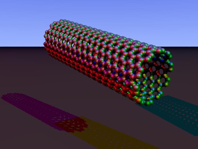
1 Nanostrukturphysik (Nanostructure Physics) Prof. Yong Lei & Dr. Yang Xu Fachgebiet 3D-Nanostrukturierung, Institut für Physik Contact: Office: Unterpoerlitzer Straße 38 (Heisenbergbau) (tel: 3748) Vorlesung: Thursday 7:00 8:30, F 3001 (Faradaybau) Übung: Friday (G), 11:00 12:30, C 110 (a) (b 1 ) (b 2 ) UTAM-prepared free-standing one-dimensional surface nanostructures on Si substrates: Ni nanowire arrays (a) and carbon nanotube arrays (b).
2 Class 1: A general introduction of fundamentals of nano-structured materials Class 2: Structures and properties of nanocrystalline materials Class 3: Graphene Class 4: 2D atomically thin nanosheets Class 5: Optical properties of 1D nanostructures and nano-generator Class 6: Carbon nanotubes Class 7: Solar water splitting I: fundamentals Class 8: Solar water splitting II: nanostructures for water splitting Class 9: Lithium-ion batteries: Si nanostructures Class 10: Sodium-ion batteries and other ion batteries, and Supercapacitors Class 11: Solar cells Class 12: Other nanostructures
3 Contents of Class 3 Graphene
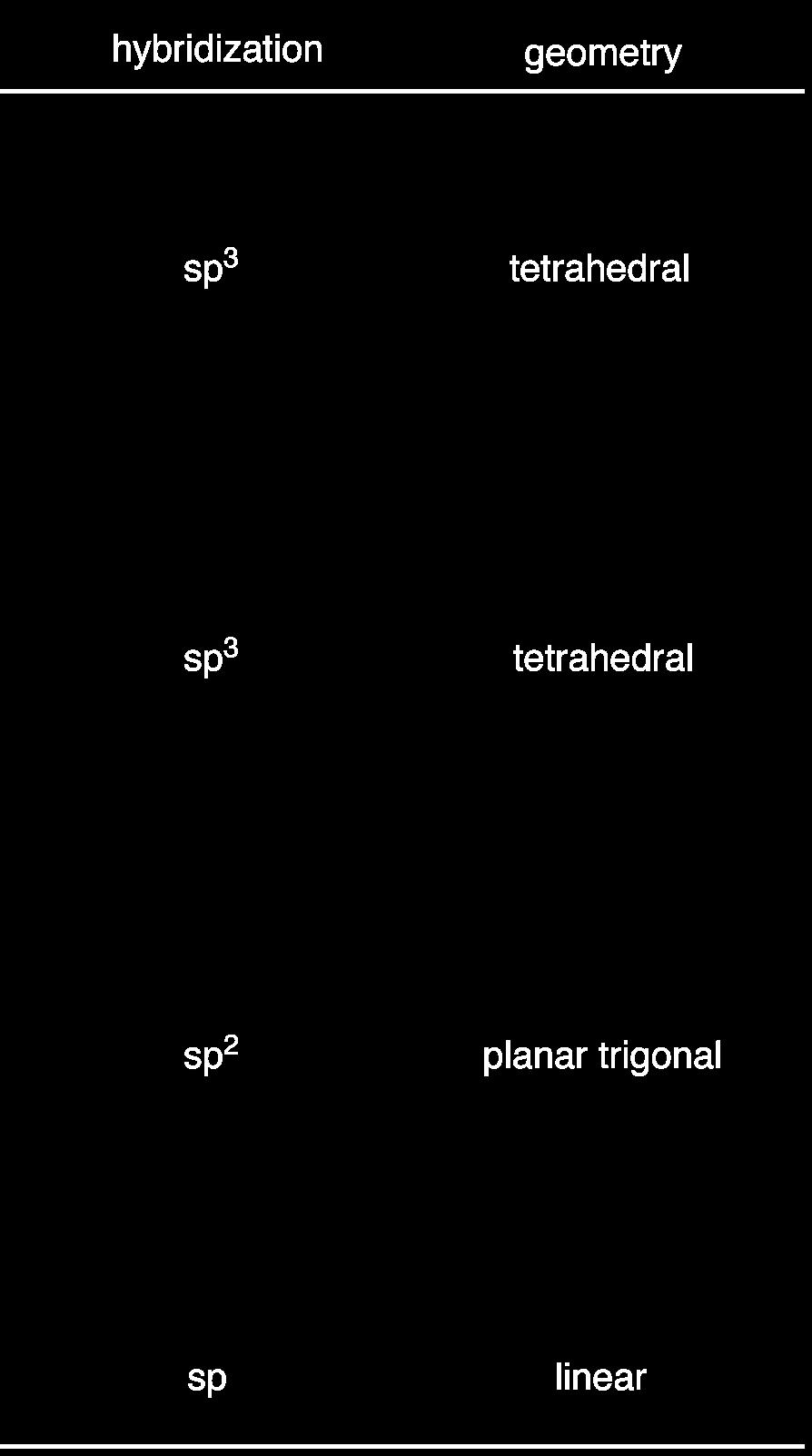
4 Graphene: honeycomb carbon Introduction Brief history Mechanical exfoliation Alternatives to mechanical exfoliation Characterizing graphene flakes Devices with graphene

5 Carbon allotropes Chem. Rev. 2015, 115, Page 5
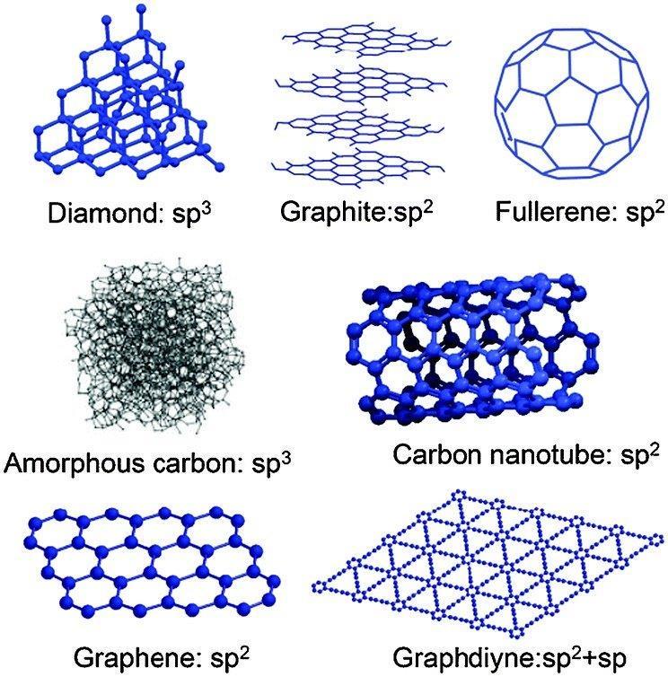
6 Carbon allotropes Page 6


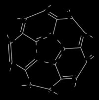
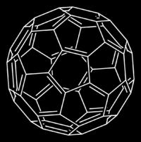
7 Fullerene: The Nobel Prize in Chemistry 1996 Robert F. Curl Jr. Sir Harold W. Kroto Richard E. Smalley The Nobel Prize in Chemistry 1996 was awarded jointly to Robert F. Curl Jr., Sir Harold W. Kroto and Richard E. Smalley "for their discovery of fullerenes" Page 7

8 Discovery of fullerenes laser evaporation of graphite Page 8


9 Fullerenes based acceptors for heterojunction organic solar cells Functionalization Page 9


10 Page 10 Carbon nanotubes


11 Graphene: The Nobel Prize in Physics 2010 Andre Geim Konstantin Novoselov for groundbreaking experiments regarding the two-dimensional material graphene Page 11

12 Graphene is a 1-atom thickness sheet of sp 2 -bonded carbon atoms that are densely packed in a honeycomb crystal lattice. Graphite consists of many graphene sheets stacked together. (


13 Graphite to Graphene Exfoliation Page 13

 306, 666;")
 102, 10451. 04.05.2018 Page 14")
14 Graphene: The Nobel Prize in Physics 2010 Highly oriented pyrolytic graphite (HOPG) Science (2004) 306, 666; Proc. Natl. Acad. Sci. (2005) 102, Page 14


15 D.I.Y. Graphene from graphite: top-down approach Page 15

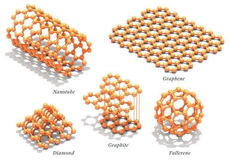
16 Graphene The Mother Of All Graphites Graphene: a single layer of carbon packed in hexagonal lattice, with a carbon-carbon distance of nm. Graphene: a basic building block for carbon materials of all other dimensions: wrap up into 0D fullerene roll up into 1D nanotubes stacked into 3D graphite A.K. Geim & K.S. Novoselov, Nat. Mater. 2017, 6, Page 16


17 Zigzag carbon nanotube could be either semiconducting or metallic


18 Armchair carbon nanotube all metallic
19 Alternatives to mechanical exfoliation Requirements A process must produce high quality in the 2D crystal lattice to ensure high mobility The method must provide fine control over crystallite thickness so as to deliver uniform device performance Alternatives Chemical exfoliation Total organic synthesis Epitaxial growth and chemical vapor deposition

20 Synthesis of Graphene Page 20
 functionalities introduced during oxidation.")
21 Chemically derived graphene from graphite oxide Chemical modification of graphite to produce a water dispersible graphene oxide (GO) Complete exfoliation of GO upon addition of mechanical energy This is due to strength of interactions between water and oxygencontaining (epoxide and hydroxyl) functionalities introduced during oxidation. Hydrophilic property leads water to readily being inserted between sheets and disperse them as individuals. Nat. Nanotechnol. 2009, 4, 25.

22 Cross-sectional SEM image of GO stacking in a film produced by filtration. Nature 2007, 448, 457. Chemical reduction produces a film with shiny color. Science 2008, 320, 1170.


23 Chemical synthesis of Graphene: Hummers method Most widely used for producing graphene by oxidizing graphite to GO by using suitable oxidizing agents. GO is then reduced to produce graphene Page 23
 of")


24 Chemical vapor deposition (CVD) of Graphene Cu or Ni foil Science 2009;324, 1312; Nature 2009, 457, Page 24


25 Page 25 Science 2009;324, 1312; Nature 2009, 457, 706.


26 CVD of Graphene foam Nature Materials 2011, 10, Page 26


27 Graphene foam via CVD A mm 2 free-standing graphene foam Nature Materials 2011, 10, Page 27
")
 chemical removal of")

28 CVD Growth of Graphene with Ni Nanowires Formation of graphene tubular structure: (a) Ni nanowire; (b) graphene grown on Ni nanowire template; (c) chemical removal of Ni nanowire. 2 layers 3 layers 5 layers 10 layers Nano Lett. 2010, 10, Page 28


29 Synthesis of Graphene Science 2008, 319, Nature 2009, 458, Page 29
 is")

30 Epitaxial graphene Substrate-based methods Epitaxial growth: silicon carbide (SiC) is reduced to graphene as silicon sublimes at high temperature. J. Phys. Chem. Solids 2006, 67, 2172.

31 Comparison of different methods for graphene mass-production Nature, 2012, 490, Page 31

32 Basic properties of Graphene Graphene's unique electronic structure enables this extraordinary material to break many records of strength, electricity and heat conduction. Density of graphene: 0.77 mg m -2 Almost optical transparent: absorbs only 2.3% of light intensity, independent of the wavelength in optical domain. Young s modulus of 1 Tera-Pascal and intrinsic strength of 130 Giga- Pascal, more than 100 times stronger than the strongest steel. RT electron mobility: μ = 200,000 cm 2 V 1 s 1. Very high thermal conductivity: ~ 3000 W m K 1, 10 times better than copper Page 32

33 Energy band structure of graphene The valence band (lower band) and conduction band (upper band) of graphene touch at six points (Brillouin zone corners), thus making graphene a zero-band-gap semiconductor. More details: The electronic properties of graphene, A. H. Castro Neto, F. Guinea, N. M. R. Peres, K. S. Novoselov, and A. K. Geim, Rev. Mod. Phys. 2009, 81, Page 33

34 Graphene: zero-band-gap semiconductor Because of its symmetrical structure its atoms scatter electrons in such a way that they cancel each other out, graphene has no electronic band gap, which is the key semiconductoring property controlling the operations of transistors, lasers, and other solid-state devices Page 34

35 Widely tunable bandgap in bilayer graphene Graphene lacks a band gap because of its symmetrical structure its atoms scatter electrons in such a way that they cancel each other out. The introduction of an electric field perpendicular to the layers creates an asymmetry, which generates a band gap. Though small, the gap is tunable, creating possibilities for new devices. Nature Nanotechnology 5, 32 (2009); Nature 459, 820 (2009) Page 35

36 Chemical doping for band gap tuning in graphene The band structure near the Dirac point of bilayer epitaxial graphene grown on the surface of SiC can be easily tuned by potassium doping. Science 2006, 313, J. Mater. Chem., 2011, 21, Page 36

37 Characterizing graphene flakes Optical Scanning probe microscopy: AFM and STM Raman spectroscopy Optical absorbance: 2.3% per layer Science 2008, 320, 1308.

38 Graphite: showing three carbons that eclipse a neighbor in the sheet directly below. Graphene: all six carbons are equivalent and thus visible. Proc. Natl. Acad. Sci. U.S.A. 2007, 104, 9209.
39 Intensity: ¼ and ½ of the G peak 3-5 cm -1 higher G band (near 1584 cm -1 ): E 2g vibrational mode G band (near 2700 cm -1 ): second-order two-phonon mode Intensity: 4 times of the G peak Phys. Rev. Lett. 2006, 97,

40 Page 40 Applications of graphene
41 1.Create rugged sensors 2.Sequence DNA 3.Re-imagine aircraft design 4.Detect concealed weapons 5.Build better electronics 6.Ramp up the performance of supercapacitors and batteries 7.Design new types of batteries 8.Kill E. coli bacterio 9.Print electronic devices 10.Soak up arsenic Page 41
42 11. Improve electron sources 12. Make high-performance modulators 13. Store hydrogen 14. Remove water from a mixture 15. Remove water from a mixture 16. Remove unwanted heat from electronics 17. Form transparent electrodes for displays 18. Make rare-element-free magnets 19. Store data 20. Harness energy from the Sun Page 42
43 Devices: single molecule detection Chemical sensors 2D structure: absolute maximum of the surface area to volume ratio in a layered material High sensitivity, every adsorption event is significant Either electron withdrawing or donating groups can lead to chemical gating of the material, which can be easily monitored in a resistive-type sensor setup. Nat. Mater. 2007, 6, 652.

44 Graphene transistor with new operating principle Graphene in a switching transistor: electric current can t be sufficiently interrupted (no band gap). A new operating principle performing switching operation with a small band gap is required: 2 top gates are placed on graphene (irradiated via He ion beam to introduce crystalline defects. Gate biases applied to 2 top gates, allowing carrier densities in top-gated graphene regions be effectively controlled. Its transistor polarity be electrically controlled and inverted (new) Page 44

45 Graphene for energy conversion and storage Nanoscale, 2013, 5, Page 45
. 04.")
46 Graphene as electrode materials for supercapacitors Graphene as electrode materials for supercapacitors: energy storage mechanism is: charges are electrochemically stored through the adsorption-desorption of electrolyte ions on the surface of graphene, socalled electric double-layer capacitors (EDLC) Page 46

47 Graphene-based supercapacitor: hummers method TEM SEM High-performance supercapacitors based on graphene for efficient energy storage under extreme environmental temperatures, a wide range of temperatures from -20 ºC to 45 ºC. Vellacheri R., Al-Haddad A., Zhao H.P., Wang W.X., Wang C.L., Lei Y.*, Nano Energy, 2014, 8, Page 47

48 Page 48


49 PECVD Growth of Vertically Oriented Graphene Carbon sources: C2H2 or CH4 Plasma gas: H2 or Ar Page 49
50 Vertically Oriented Graphene for Supercapacitors Supercapacitors have a very fast response time (sub-millisecond timescale). Supercapacitors via vertically oriented graphene could be charged and discharged in less than a millisecond, This ultrafast supercapacitor could replace the large electrolytic capacitors used in today s electronics and may someday help make electronic devices smaller and lighter. Science 2010, 329, Page 50

51 Graphene-nanotube 3D architecture for dye-sensitized solar cells Science Advance 2015,1, Showed a power conversion efficiency of 6.8 % and out-performed the counterparts with an expensive Pt wire counter electrode by a factor of Page 51

52 Graphene as electrode materials for batteries Graphene is a great substrate for LIB anode and cathode materials to create highenergy-density, fast-charging and longer-lasting batteries. Although graphite is an excellent anode in LIBs, it cannot be utilized in Na + and Al 3+ batteries because these ions are too large to effectively insert into graphite, so alternative anode materials are required, such as porous graphene composites Page 52
53 Graphene in bio-applications In addition to electronics and photonics, graphene also has great potentials in bio-applications, such as drug delivery, tissue engineering, biosensors. Graphene sheets are highly hydrophobic and tend to aggregate, exhibiting a low water dispersibility, thus are not suitable for direct bio-applications. Chem. Soc. Rev., 2017, 46, Page 53
54 Graphene in bio-applications Graphene oxide (GO) can be easily synthesized by Hummers method, offers a richer surface chemistry due to the presence of the oxide groups. Reduced graphene oxide (rgo): chemically reduced GO to remove oxygen functional groups. rgo can be considered as an intermediate structure between the graphene sheet and the highly-oxidized GO. GO and rgo can be more easily handled, especially in liquids, since they generally exhibit good water dispersibility and a very rich surface chemistry, which allows a wide range of biomedical applications. Chem. Soc. Rev., 2017, 46, Page 54

55 Graphene in biomedical applications Drug delivery Chem. Soc. Rev., 2017, 46, Page 55

56 Graphene in biomedical applications Biosensors Chem. Soc. Rev., 2017, 46, Page 56
57 Class 1: A general introduction of fundamentals of nano-structured materials Class 2: Structures and properties of nanocrystalline materials Class 3: Graphene Class 4: 2D atomically thin nanosheets Class 5: Optical properties of 1D nanostructures and nano-generator Class 6: Carbon nanotubes Class 7: Solar water splitting I: fundamentals Class 8: Solar water splitting II: nanostructures for water splitting Class 9: Lithium-ion batteries: Si nanostructures Class 10: Sodium-ion batteries and other ion batteries, and Supercapacitors Class 11: Solar cells Class 12: Other nanostructures
58 Thank you!
Halbleiter Prof. Yong Lei Prof. Thomas Hannappel
 Halbleiter Prof. Yong Lei Prof. Thomas Hannappel yong.lei@tu-ilmenau.de thomas.hannappel@tu-ilmenau.de http:///nanostruk/ Organic semiconductors Small-molecular materials Rubrene Pentacene Polymers PEDOT:PSS
Nanostrukturphysik Übung 2 (Class 3&4)
") Nanostrukturphysik Übung 2 (Class 3&4) Prof. Yong Lei & Dr. Yang Xu 2017.05.03 Fachgebiet 3D-Nanostrukturierung, Institut für Physik Contact: yong.lei@tu-ilmenau.de (3748), yang.xu@tuilmenau.de (4902)
Nanostrukturphysik Übung 2 (Class 3&4) Prof. Yong Lei & Dr. Yang Xu 2017.05.03 Fachgebiet 3D-Nanostrukturierung, Institut für Physik Contact: yong.lei@tu-ilmenau.de (3748), yang.xu@tuilmenau.de (4902)
Nanostrukturphysik (Nanostructure Physics)
") Nanostrukturphysik (Nanostructure Physics) Prof. Yong Lei & Dr. Yang Xu Fachgebiet 3D-Nanostrukturierung, Institut für Physik Contact: yong.lei@tu-ilmenau.de; yang.xu@tu-ilmenau.de Office: Unterpoerlitzer
Nanostrukturphysik (Nanostructure Physics) Prof. Yong Lei & Dr. Yang Xu Fachgebiet 3D-Nanostrukturierung, Institut für Physik Contact: yong.lei@tu-ilmenau.de; yang.xu@tu-ilmenau.de Office: Unterpoerlitzer
Graphene. Tianyu Ye November 30th, 2011
 Graphene Tianyu Ye November 30th, 2011 Outline What is graphene? How to make graphene? (Exfoliation, Epitaxial, CVD) Is it graphene? (Identification methods) Transport properties; Other properties; Applications;
Graphene films on silicon carbide (SiC) wafers supplied by Nitride Crystals, Inc.
 wafers supplied by Nitride Crystals, Inc.") 9702 Gayton Road, Suite 320, Richmond, VA 23238, USA Phone: +1 (804) 709-6696 info@nitride-crystals.com www.nitride-crystals.com Graphene films on silicon carbide (SiC) wafers supplied by Nitride Crystals,
9702 Gayton Road, Suite 320, Richmond, VA 23238, USA Phone: +1 (804) 709-6696 info@nitride-crystals.com www.nitride-crystals.com Graphene films on silicon carbide (SiC) wafers supplied by Nitride Crystals,
Carbon nanomaterials. Gavin Lawes Wayne State University.
 Carbon nanomaterials Gavin Lawes Wayne State University glawes@wayne.edu Outline 1. Carbon structures 2. Carbon nanostructures 3. Potential applications for Carbon nanostructures Periodic table from bpc.edu
Nanostrukturphysik (Nanostructure Physics)
") Nanostrukturphysik (Nanostructure Physics) Prof. Yong Lei & Dr. Huaping Zhao Fachgebiet Angewandte Nanophysik, Institut für Physik Contact: yong.lei@tu-ilmenau.de; huaping.zhao@tu-ilmenau.de Office: Unterpoerlitzer
Nanostrukturphysik (Nanostructure Physics) Prof. Yong Lei & Dr. Huaping Zhao Fachgebiet Angewandte Nanophysik, Institut für Physik Contact: yong.lei@tu-ilmenau.de; huaping.zhao@tu-ilmenau.de Office: Unterpoerlitzer
Graphene Fundamentals and Emergent Applications
 Graphene Fundamentals and Emergent Applications Jamie H. Warner Department of Materials University of Oxford Oxford, UK Franziska Schaffel Department of Materials University of Oxford Oxford, UK Alicja
Initial Stages of Growth of Organic Semiconductors on Graphene
 Initial Stages of Growth of Organic Semiconductors on Graphene Presented by: Manisha Chhikara Supervisor: Prof. Dr. Gvido Bratina University of Nova Gorica Outline Introduction to Graphene Fabrication
Lectures Graphene and
 Lectures 15-16 Graphene and carbon nanotubes Graphene is atomically thin crystal of carbon which is stronger than steel but flexible, is transparent for light, and conducts electricity (gapless semiconductor).
CVD growth of Graphene. SPE ACCE presentation Carter Kittrell James M. Tour group September 9 to 11, 2014
 CVD growth of Graphene SPE ACCE presentation Carter Kittrell James M. Tour group September 9 to 11, 2014 Graphene zigzag armchair History 1500: Pencil-Is it made of lead? 1789: Graphite 1987: The first
Overview. Carbon in all its forms. Background & Discovery Fabrication. Important properties. Summary & References. Overview of current research
 Graphene Prepared for Solid State Physics II Pr Dagotto Spring 2009 Laurene Tetard 03/23/09 Overview Carbon in all its forms Background & Discovery Fabrication Important properties Overview of current
Wafer-scale fabrication of graphene
 Wafer-scale fabrication of graphene Sten Vollebregt, MSc Delft University of Technology, Delft Institute of Mircosystems and Nanotechnology Delft University of Technology Challenge the future Delft University
Nanostrukturphysik (Nanostructure Physics)
") Nanostrukturphysik (Nanostructure Physics) Prof. Yong Lei & Dr. Yang Xu Fachgebiet 3D-Nanostrukturierung, Institut für Physik Contact: yong.lei@tu-ilmenau.de; yang.xu@tu-ilmenau.de Office: Unterpoerlitzer
Nanostrukturphysik (Nanostructure Physics) Prof. Yong Lei & Dr. Yang Xu Fachgebiet 3D-Nanostrukturierung, Institut für Physik Contact: yong.lei@tu-ilmenau.de; yang.xu@tu-ilmenau.de Office: Unterpoerlitzer
Conference Return Seminar- NANO2014,Moscow State University,Moscow,Russia Date: th July 2014
 Conference Return Seminar- NANO2014,Moscow State University,Moscow,Russia Date:13-1818 th July 2014 An electrochemical method for the synthesis of single and few layers graphene sheets for high temperature
Techniken der Oberflächenphysik (Techniques of Surface Physics)
") Techniken der Oberflächenphysik (Techniques of Surface Physics) Prof. Yong Lei & Dr. Yang Xu, Dr. Huaping Zhao Fachgebiet Angewante Nanophysik, Institut für Physik Contact: yong.lei@tu-ilmenau.de yang.xu@tu-ilmenau.de
Techniken der Oberflächenphysik (Techniques of Surface Physics) Prof. Yong Lei & Dr. Yang Xu, Dr. Huaping Zhao Fachgebiet Angewante Nanophysik, Institut für Physik Contact: yong.lei@tu-ilmenau.de yang.xu@tu-ilmenau.de
Nanostrukturphysik (Nanostructure Physics)
") Nanostrukturphysik (Nanostructure Physics) Prof. Yong Lei & Dr. Yang Xu Fachgebiet 3D-Nanostrukturierung, Institut für Physik Contact: yong.lei@tu-ilmenau.de; yang.xu@tu-ilmenau.de Office: Unterpoerlitzer
Nanostrukturphysik (Nanostructure Physics) Prof. Yong Lei & Dr. Yang Xu Fachgebiet 3D-Nanostrukturierung, Institut für Physik Contact: yong.lei@tu-ilmenau.de; yang.xu@tu-ilmenau.de Office: Unterpoerlitzer
Techniken der Oberflächenphysik (Technique of Surface Physics)
") Techniken der Oberflächenphysik (Technique of Surface Physics) Yong Lei & Fabian Grote Fachgebiet 3D-Nanostrukturierung, Institut für Physik Contact: yong.lei@tu-ilmenau.de; fabian.grote@tu-ilmenau.de
Techniken der Oberflächenphysik (Technique of Surface Physics) Yong Lei & Fabian Grote Fachgebiet 3D-Nanostrukturierung, Institut für Physik Contact: yong.lei@tu-ilmenau.de; fabian.grote@tu-ilmenau.de
Seminars in Nanosystems - I
 Seminars in Nanosystems - I Winter Semester 2011/2012 Dr. Emanuela Margapoti Emanuela.Margapoti@wsi.tum.de Dr. Gregor Koblmüller Gregor.Koblmueller@wsi.tum.de Seminar Room at ZNN 1 floor Topics of the
STM and graphene. W. W. Larry Pai ( 白偉武 ) Center for condensed matter sciences, National Taiwan University NTHU, 2013/05/23
 Center for condensed matter sciences, National Taiwan University NTHU, 2013/05/23") STM and graphene W. W. Larry Pai ( 白偉武 ) Center for condensed matter sciences, National Taiwan University NTHU, 2013/05/23 Why graphene is important: It is a new form of material (two dimensional, single
STM and graphene W. W. Larry Pai ( 白偉武 ) Center for condensed matter sciences, National Taiwan University NTHU, 2013/05/23 Why graphene is important: It is a new form of material (two dimensional, single
Transparent Electrode Applications
 Transparent Electrode Applications LCD Solar Cells Touch Screen Indium Tin Oxide (ITO) Zinc Oxide (ZnO) - High conductivity - High transparency - Resistant to environmental effects - Rare material (Indium)
1. Nanotechnology & nanomaterials -- Functional nanomaterials enabled by nanotechnologies.
 Novel Nano-Engineered Semiconductors for Possible Photon Sources and Detectors NAI-CHANG YEH Department of Physics, California Institute of Technology 1. Nanotechnology & nanomaterials -- Functional nanomaterials
3-month progress Report
 3-month progress Report Graphene Devices and Circuits Supervisor Dr. P.A Childs Table of Content Abstract... 1 1. Introduction... 1 1.1 Graphene gold rush... 1 1.2 Properties of graphene... 3 1.3 Semiconductor
The many forms of carbon
 The many forms of carbon Carbon is not only the basis of life, it also provides an enormous variety of structures for nanotechnology. This versatility is connected to the ability of carbon to form two
Carbon Nanomaterials: Nanotubes and Nanobuds and Graphene towards new products 2030
 Carbon Nanomaterials: Nanotubes and Nanobuds and Graphene towards new products 2030 Prof. Dr. Esko I. Kauppinen Helsinki University of Technology (TKK) Espoo, Finland Forecast Seminar February 13, 2009
Supporting Information Available:
 Supporting Information Available: Photoresponsive and Gas Sensing Field-Effect Transistors based on Multilayer WS 2 Nanoflakes Nengjie Huo 1, Shengxue Yang 1, Zhongming Wei 2, Shu-Shen Li 1, Jian-Bai Xia
performance electrocatalytic or electrochemical devices. Nanocrystals grown on graphene could have
 Nanocrystal Growth on Graphene with Various Degrees of Oxidation Hailiang Wang, Joshua Tucker Robinson, Georgi Diankov, and Hongjie Dai * Department of Chemistry and Laboratory for Advanced Materials,
GRAPHENE ON THE Si-FACE OF SILICON CARBIDE USER MANUAL
 GRAPHENE ON THE Si-FACE OF SILICON CARBIDE USER MANUAL 1. INTRODUCTION Silicon Carbide (SiC) is a wide band gap semiconductor that exists in different polytypes. The substrate used for the fabrication
Graphene FETs EE439 FINAL PROJECT. Yiwen Meng Su Ai
 Graphene FETs EE439 FINAL PROJECT Yiwen Meng Su Ai Introduction What is Graphene? An atomic-scale honeycomb lattice made of carbon atoms Before 2004, Hypothetical Carbon Structure Until 2004, physicists
Nanostrukturphysik. Prof. Yong Lei & Dr. Yang Xu Fachgebiet 3D-Nanostrukturierung, Institut für Physik
 Nanostrukturphysik Prof. Yong Lei & Dr. Yang Xu Fachgebiet 3D-Nanostrukturierung, Institut für Physik Contact: yong.lei@tu-ilmenau.de (3748), yang.xu@tuilmenau.de (4902) Office: Gebäude V202, Unterpörlitzer
Black phosphorus: A new bandgap tuning knob
 Black phosphorus: A new bandgap tuning knob Rafael Roldán and Andres Castellanos-Gomez Modern electronics rely on devices whose functionality can be adjusted by the end-user with an external knob. A new
Nanostructures. Lecture 13 OUTLINE
 Nanostructures MTX9100 Nanomaterials Lecture 13 OUTLINE -What is quantum confinement? - How can zero-dimensional materials be used? -What are one dimensional structures? -Why does graphene attract so much
Supplementary Figure S1. AFM images of GraNRs grown with standard growth process. Each of these pictures show GraNRs prepared independently,
 Supplementary Figure S1. AFM images of GraNRs grown with standard growth process. Each of these pictures show GraNRs prepared independently, suggesting that the results is reproducible. Supplementary Figure
Graphene and Carbon Nanotubes
 Graphene and Carbon Nanotubes 1 atom thick films of graphite atomic chicken wire Novoselov et al - Science 306, 666 (004) 100μm Geim s group at Manchester Novoselov et al - Nature 438, 197 (005) Kim-Stormer
Grpahene Synthesis by CVD. QingkaiYu Ingram School of Engineering Texas State University at San Marcos
 Grpahene Synthesis by CVD QingkaiYu Ingram School of Engineering Texas State University at San Marcos @ Applied Nanotech Inc, July 25 th, 2011 Acknowledgement Texas State University Dr. Zhihong Liu Austin
Graphene: the Route from Touch Screens to Digital Nanoelectronics
 Graphene: the Route from Touch Screens to Digital Nanoelectronics László Péter Biró Research Institute for Technical Physics & Materials Science, Budapest, Hungary http://www.nanotechnology.hu/ Human History
SUPPLEMENTARY INFORMATION
 SUPPLEMENTARY INFORMATION Facile Synthesis of High Quality Graphene Nanoribbons Liying Jiao, Xinran Wang, Georgi Diankov, Hailiang Wang & Hongjie Dai* Supplementary Information 1. Photograph of graphene
Introduction to Nanotechnology Chapter 5 Carbon Nanostructures Lecture 1
 Introduction to Nanotechnology Chapter 5 Carbon Nanostructures Lecture 1 ChiiDong Chen Institute of Physics, Academia Sinica chiidong@phys.sinica.edu.tw 02 27896766 Section 5.2.1 Nature of the Carbon Bond
Solutions for Assignment-8
 Solutions for Assignment-8 Q1. The process of adding impurities to a pure semiconductor is called: [1] (a) Mixing (b) Doping (c) Diffusing (d) None of the above In semiconductor production, doping intentionally
Imaging Carbon materials with correlative Raman-SEM microscopy. Introduction. Raman, SEM and FIB within one chamber. Diamond.
 Imaging Carbon materials with correlative Raman-SEM microscopy Application Example Carbon materials are widely used in many industries for their exceptional properties. Electric conductance, light weight,
Halbleiter. Prof. Yong Lei. Prof. Thomas Hannappel.
 Halbleiter Prof. Yong Lei Prof. Thomas Hannappel yong.lei@tu-ilemnau.de thomas.hannappel@tu-ilmenau.de Important Events in Semiconductors History 1833 Michael Faraday discovered temperature-dependent conductivity
GRAPHENE NANORIBBONS Nahid Shayesteh,
 USC Department of Physics Graduate Seminar 1 GRAPHENE NANORIBBONS Nahid Shayesteh, Outlines 2 Carbon based material Discovery and innovation of graphen Graphene nanoribbons structure Application of Graphene
In today s lecture, we will cover:
 In today s lecture, we will cover: Metal and Metal oxide Nanoparticles Semiconductor Nanocrystals Carbon Nanotubes 1 Week 2: Nanoparticles Goals for this section Develop an understanding of the physical
Carbon Nanotubes (CNTs)
") Carbon Nanotubes (s) Seminar: Quantendynamik in mesoskopischen Systemen Florian Figge Fakultät für Physik Albert-Ludwigs-Universität Freiburg July 7th, 2010 F. Figge (University of Freiburg) Carbon Nanotubes
Carbon Nanotubes (s) Seminar: Quantendynamik in mesoskopischen Systemen Florian Figge Fakultät für Physik Albert-Ludwigs-Universität Freiburg July 7th, 2010 F. Figge (University of Freiburg) Carbon Nanotubes
Part II. Introduction of Graphene
 Part II. Introduction of Graphene 1 Graphene (Mother of all graphitic form) 2D honeycomb lattice Graphene 0D 1D 3D bulky bll ball Nanotube Graphite Geims et al, Nature Materials,Vol.6 183, 2007 2 History
Chapter - 8. Summary and Conclusion
 Chapter - 8 Summary and Conclusion The present research explains the synthesis process of two transition metal oxide semiconductors SnO 2 and V 2 O 5 thin films with different morphologies and studies
From nanophysics research labs to cell phones. Dr. András Halbritter Department of Physics associate professor
 From nanophysics research labs to cell phones Dr. András Halbritter Department of Physics associate professor Curriculum Vitae Birth: 1976. High-school graduation: 1994. Master degree: 1999. PhD: 2003.
The goal of this project is to enhance the power density and lowtemperature efficiency of solid oxide fuel cells (SOFC) manufactured by atomic layer
 manufactured by atomic layer") Stanford University Michael Shandalov1, Shriram Ramanathan2, Changhyun Ko2 and Paul McIntyre1 1Department of Materials Science and Engineering, Stanford University 2Division of Engineering and Applied
Stanford University Michael Shandalov1, Shriram Ramanathan2, Changhyun Ko2 and Paul McIntyre1 1Department of Materials Science and Engineering, Stanford University 2Division of Engineering and Applied
Plastic Electronics. Joaquim Puigdollers.
 Plastic Electronics Joaquim Puigdollers Joaquim.puigdollers@upc.edu Nobel Prize Chemistry 2000 Origins Technological Interest First products.. MONOCROMATIC PHILIPS Today Future Technological interest Low
Carbon Nanotubes. Andrea Goldoni. Elettra- Sincrotrone Trieste S.C.p.A., s.s. 14 Km 163,5 in Area Science Park, Trieste, Italy
 Carbon Nanotubes Andrea Goldoni Elettra- Sincrotrone Trieste S.C.p.A., s.s. 14 Km 163,5 in Area Science Park, 34012 Trieste, Italy Up to 1985 the only two allotropic form of carbon were known: graphite
Supplementary Figure 1 Dark-field optical images of as prepared PMMA-assisted transferred CVD graphene films on silicon substrates (a) and the one
 and the one") Supplementary Figure 1 Dark-field optical images of as prepared PMMA-assisted transferred CVD graphene films on silicon substrates (a) and the one after PBASE monolayer growth (b). 1 Supplementary Figure
Supplementary Figure 1 Dark-field optical images of as prepared PMMA-assisted transferred CVD graphene films on silicon substrates (a) and the one after PBASE monolayer growth (b). 1 Supplementary Figure
Graphene: Plane and Simple Electrical Metrology?
 Graphene: Plane and Simple Electrical Metrology? R. E. Elmquist, F. L. Hernandez-Marquez, M. Real, T. Shen, D. B. Newell, C. J. Jacob, and G. R. Jones, Jr. National Institute of Standards and Technology,
Supplementary Figure 1 Experimental setup for crystal growth. Schematic drawing of the experimental setup for C 8 -BTBT crystal growth.
 Supplementary Figure 1 Experimental setup for crystal growth. Schematic drawing of the experimental setup for C 8 -BTBT crystal growth. Supplementary Figure 2 AFM study of the C 8 -BTBT crystal growth
XPS Depth Profiling of Epitaxial Graphene Intercalated with FeCl 3
 XPS Depth Profiling of Epitaxial Graphene Intercalated with FeCl 3 Mahdi Ibrahim Maynard H. Jackson High School Atlanta, GA. Faculty Advisor: Dr. Kristin Shepperd Research Group: Prof. Edward Conrad School
Carbon Structure Simulations using Crystal Viewer Tool
 Carbon Structure Simulations using Crystal Viewer Tool The Crystal Viewer tool in nanohub.org can be used to build three carbon nanostructures: graphene sheets, Buckminsterfullerene, Bucky balls (C 60
e - Galvanic Cell 1. Voltage Sources 1.1 Polymer Electrolyte Membrane (PEM) Fuel Cell
 Fuel Cell") Galvanic cells convert different forms of energy (chemical fuel, sunlight, mechanical pressure, etc.) into electrical energy and heat. In this lecture, we are interested in some examples of galvanic cells.
Galvanic cells convert different forms of energy (chemical fuel, sunlight, mechanical pressure, etc.) into electrical energy and heat. In this lecture, we are interested in some examples of galvanic cells.
Chapter 1 Introduction
 Chapter 1 Introduction In our planet carbon forms the basis of all organic molecules which makes it the most important element of life. It is present in over 95% of the known chemical compounds overall
Nanotechnology in Consumer Products
 Nanotechnology in Consumer Products June 17, 2015 October 31, 2014 The webinar will begin at 1pm Eastern Time Perform an audio check by going to Tools > Audio > Audio Setup Wizard Chat Box Chat Box Send
A. Optimizing the growth conditions of large-scale graphene films
 1 A. Optimizing the growth conditions of large-scale graphene films Figure S1. Optical microscope images of graphene films transferred on 300 nm SiO 2 /Si substrates. a, Images of the graphene films grown
Chapter 12: Structures & Properties of Ceramics
 Chapter 12: Structures & Properties of Ceramics ISSUES TO ADDRESS... How do the crystal structures of ceramic materials differ from those for metals? How do point defects in ceramics differ from those
per unit cell Motif: Re at (0, 0, 0); 3O at ( 1 / 2, 0), (0, 0, 1 / 2 ) Re: 6 (octahedral coordination) O: 2 (linear coordination) ReO 6
; 3O at ( 1 / 2, 0), (0, 0, 1 / 2 ) Re: 6 (octahedral coordination) O: 2 (linear coordination) ReO 6") Lattice: Primitive Cubic 1ReO 3 per unit cell Motif: Re at (0, 0, 0); 3O at ( 1 / 2, 0, 0), (0, 1 / 2, 0), (0, 0, 1 / 2 ) Re: 6 (octahedral coordination) O: 2 (linear coordination) ReO 6 octahedra share
Lattice: Primitive Cubic 1ReO 3 per unit cell Motif: Re at (0, 0, 0); 3O at ( 1 / 2, 0, 0), (0, 1 / 2, 0), (0, 0, 1 / 2 ) Re: 6 (octahedral coordination) O: 2 (linear coordination) ReO 6 octahedra share
Techniken der Oberflächenphysik (Techniques of Surface Physics)
") Techniken der Oberflächenphysik (Techniques of Surface Physics) Prof. Yong Lei & Dr. Yang Xu (& Liying Liang) Fachgebiet 3D-Nanostrukturierung, Institut für Physik Contact: yong.lei@tu-ilmenau.de; yang.xu@tu-ilmenau.de;
Techniken der Oberflächenphysik (Techniques of Surface Physics) Prof. Yong Lei & Dr. Yang Xu (& Liying Liang) Fachgebiet 3D-Nanostrukturierung, Institut für Physik Contact: yong.lei@tu-ilmenau.de; yang.xu@tu-ilmenau.de;
Contents. Foreword by Darrell H. Reneker
 Table of Foreword by Darrell H. Reneker Preface page xi xiii 1 Introduction 1 1.1 How big is a nanometer? 1 1.2 What is nanotechnology? 1 1.3 Historical development of nanotechnology 2 1.4 Classification
Optimizing Graphene Morphology on SiC(0001)
") Optimizing Graphene Morphology on SiC(0001) James B. Hannon Rudolf M. Tromp Graphene sheets Graphene sheets can be formed into 0D,1D, 2D, and 3D structures Chemically inert Intrinsically high carrier mobility
Optimizing Graphene Morphology on SiC(0001) James B. Hannon Rudolf M. Tromp Graphene sheets Graphene sheets can be formed into 0D,1D, 2D, and 3D structures Chemically inert Intrinsically high carrier mobility
Nanostructure. Materials Growth Characterization Fabrication. More see Waser, chapter 2
 Nanostructure Materials Growth Characterization Fabrication More see Waser, chapter 2 Materials growth - deposition deposition gas solid Physical Vapor Deposition Chemical Vapor Deposition Physical Vapor
So why is sodium a metal? Tungsten Half-filled 5d band & half-filled 6s band. Insulators. Interaction of metals with light?
 Bonding in Solids: Metals, Insulators, & CHEM 107 T. Hughbanks Delocalized bonding in Solids Think of a pure solid as a single, very large molecule. Use our bonding pictures to try to understand properties.
TRANSVERSE SPIN TRANSPORT IN GRAPHENE
 International Journal of Modern Physics B Vol. 23, Nos. 12 & 13 (2009) 2641 2646 World Scientific Publishing Company TRANSVERSE SPIN TRANSPORT IN GRAPHENE TARIQ M. G. MOHIUDDIN, A. A. ZHUKOV, D. C. ELIAS,
Supporting Information for
 Supporting Information for Multilayer CuO@NiO Hollow Spheres: Microwave-Assisted Metal-Organic-Framework Derivation and Highly Reversible Structure-Matched Stepwise Lithium Storage Wenxiang Guo, Weiwei
Why are we so excited about carbon nanostructures? Mildred Dresselhaus Massachusetts Institute of Technology Cambridge, MA
 Why are we so excited about carbon nanostructures? Mildred Dresselhaus Massachusetts Institute of Technology Cambridge, MA Conference for Undergraduate Women in Physics at Yale January 18, 2009 Why are
on Self-Assembly of Fullerene Molecules
 Effect of Surface Preparation of Copper on Self-Assembly of Fullerene Molecules Dongni Ma, Selene Sandoval, Krishna Muralidharan, Srini Raghavan University of Arizona Department of Materials Science and
Ali Ahmadpour. Fullerenes. Ali Ahmadpour. Department of Chemical Engineering Faculty of Engineering Ferdowsi University of Mashhad
 Ali Ahmadpour Fullerenes Ali Ahmadpour Department of Chemical Engineering Faculty of Engineering Ferdowsi University of Mashhad 2014 World of Carbon Materials 2 Fullerenes 1985 Robert F. Curl Jr. Richard
Layered Compounds. Two-dimensional layers. Graphite. Clay Minerals. Layered Double Hydroxides (LDHs) Layered α-zirconium Phosphates and Phosphonates
 Layered α-zirconium Phosphates and Phosphonates") Layered Compounds Two-dimensional layers Graphite Clay Minerals Layered Double Hydroxides (LDHs) Layered α-zirconium Phosphates and Phosphonates Layered Manganese Oxides Layered Metal Chalcogenides Alkali
Layered Compounds Two-dimensional layers Graphite Clay Minerals Layered Double Hydroxides (LDHs) Layered α-zirconium Phosphates and Phosphonates Layered Manganese Oxides Layered Metal Chalcogenides Alkali
Marriage of Graphene and Cellulose for Reinforced Composite Preparation Zaiton Abdul Majid, Wan Hazman Danial and Mohd Bakri Bakar
 Graphene Malaysia 2016 8-9 th Nov 2016 Marriage of Graphene and Cellulose for Reinforced Composite Preparation Zaiton Abdul Majid, Wan Hazman Danial and Mohd Bakri Bakar Graphene Synthesis Fundamental
Synthesis and Characterization of Graphene by Raman Spectroscopy
 Journal of Materials Sciences and Applications 2015; 1(3): 130-135 Published online June 20, 2015 (http://www.aascit.org/journal/jmsa) Synthesis and Characterization of Graphene by Raman Spectroscopy Hilal
Supplementary Figure 1 XPS, Raman and TGA characterizations on GO and freeze-dried HGF and GF. (a) XPS survey spectra and (b) C1s spectra.
 XPS survey spectra and (b) C1s spectra.") Supplementary Figure 1 XPS, Raman and TGA characterizations on GO and freeze-dried HGF and GF. (a) XPS survey spectra and (b) C1s spectra. (c) Raman spectra. (d) TGA curves. All results confirm efficient
Supplementary Figure 1 XPS, Raman and TGA characterizations on GO and freeze-dried HGF and GF. (a) XPS survey spectra and (b) C1s spectra. (c) Raman spectra. (d) TGA curves. All results confirm efficient
Nanostrukturphysik (Nanostructure Physics)
") Nanostrukturphysik (Nanostructure Physics) Yong Lei & Fabian Grote Fachgebiet 3D-Nanostrukturierung, Institut für Physik Contact: yong.lei@tu-ilmenau.de; fabian.grote@tu-ilmenau.de Office: Heliosbau 1102,
Nanostrukturphysik (Nanostructure Physics) Yong Lei & Fabian Grote Fachgebiet 3D-Nanostrukturierung, Institut für Physik Contact: yong.lei@tu-ilmenau.de; fabian.grote@tu-ilmenau.de Office: Heliosbau 1102,
Band-like transport in highly crystalline graphene films from
 Supplementary figures Title: Band-like transport in highly crystalline graphene films from defective graphene oxides R. Negishi 1,*, M. Akabori 2, T. Ito 3, Y. Watanabe 4 and Y. Kobayashi 1 1 Department
Physics of Nanotubes, Graphite and Graphene Mildred Dresselhaus
 Quantum Transport and Dynamics in Nanostructures The 4 th Windsor Summer School on Condensed Matter Theory 6-18 August 2007, Great Park Windsor (UK) Physics of Nanotubes, Graphite and Graphene Mildred
Supporting Information. by Hexagonal Boron Nitride
 Supporting Information High Velocity Saturation in Graphene Encapsulated by Hexagonal Boron Nitride Megan A. Yamoah 1,2,, Wenmin Yang 1,3, Eric Pop 4,5,6, David Goldhaber-Gordon 1 * 1 Department of Physics,
SCIENCE & TECHNOLOGY
 Pertanika J. Sci. & Technol. 25 (S): 205-212 (2017) SCIENCE & TECHNOLOGY Journal homepage: http://www.pertanika.upm.edu.my/ Effect of Boron and Oxygen Doping to Graphene Band Structure Siti Fazlina bt
Session V: Graphene. Matteo Bruna CAMBRIDGE UNIVERSITY DEPARTMENT OF ENGINEERING
 Session V: Graphene Matteo Bruna Graphene: Material in the Flatland Graphite Graphene Properties: Thinnest imaginable material Good(and tunable) electrical conductor Strongest ever measured Stiffest known
Energy Storage. Light-emitting. Nano-Carbons. H 2 Energy. CNT synthesis. Graphene synthesis Top-down. Solar H 2 generation
 Nano-Carbon battery Graphene synthesis Top-down CNT synthesis CVD reactor hydrocarbon gas Catalyst CNTs Chemical Modification COO O NO 2 COO COO COO Bottom-up O O NO NO 2 2 COO COO Nano-Carbons 20 nm Light-emitting
Supplementary Figure 1. Selected area electron diffraction (SAED) of bilayer graphene and tblg. (a) AB
 of bilayer graphene and tblg. (a) AB") Supplementary Figure 1. Selected area electron diffraction (SAED) of bilayer graphene and tblg. (a) AB stacked bilayer graphene (b), (c), (d), (e), and (f) are twisted bilayer graphene with twist angle
Supplementary Figure 1. Selected area electron diffraction (SAED) of bilayer graphene and tblg. (a) AB stacked bilayer graphene (b), (c), (d), (e), and (f) are twisted bilayer graphene with twist angle
Techniken der Oberflächenphysik (Techniques of Surface Physics)
") Techniken der Oberflächenphysik (Techniques of Surface Physics) Prof. Yong Lei & Dr. Yang Xu Fachgebiet 3D-Nanostrukturierung, Institut für Physik Contact: yong.lei@tu-ilmenau.de yang.xu@tu-ilmenau.de
Techniken der Oberflächenphysik (Techniques of Surface Physics) Prof. Yong Lei & Dr. Yang Xu Fachgebiet 3D-Nanostrukturierung, Institut für Physik Contact: yong.lei@tu-ilmenau.de yang.xu@tu-ilmenau.de
Raman spectroscopy at the edges of multilayer graphene
 Raman spectroscopy at the edges of multilayer graphene Q. -Q. Li, X. Zhang, W. -P. Han, Y. Lu, W. Shi, J. -B. Wu, P. -H. Tan* State Key Laboratory of Superlattices and Microstructures, Institute of Semiconductors,
Raman Imaging and Electronic Properties of Graphene
 Raman Imaging and Electronic Properties of Graphene F. Molitor, D. Graf, C. Stampfer, T. Ihn, and K. Ensslin Laboratory for Solid State Physics, ETH Zurich, 8093 Zurich, Switzerland ensslin@phys.ethz.ch
Supplemental Information. Lightweight Metallic MgB 2 Mediates. Polysulfide Redox and Promises High- Energy-Density Lithium-Sulfur Batteries
 JOUL, Volume 3 Supplemental Information Lightweight Metallic MgB 2 Mediates Polysulfide Redox and Promises High- Energy-Density Lithium-Sulfur Batteries Quan Pang, Chun Yuen Kwok, Dipan Kundu, Xiao Liang,
Carbon Nanomaterials
 Carbon Nanomaterials STM Image 7 nm AFM Image Fullerenes C 60 was established by mass spectrographic analysis by Kroto and Smalley in 1985 C 60 is called a buckminsterfullerene or buckyball due to resemblance
2D MBE Activities in Sheffield. I. Farrer, J. Heffernan Electronic and Electrical Engineering The University of Sheffield
 2D MBE Activities in Sheffield I. Farrer, J. Heffernan Electronic and Electrical Engineering The University of Sheffield Outline Motivation Van der Waals crystals The Transition Metal Di-Chalcogenides
A new method of growing graphene on Cu by hydrogen etching
 A new method of growing graphene on Cu by hydrogen etching Linjie zhan version 6, 2015.05.12--2015.05.24 CVD graphene Hydrogen etching Anisotropic Copper-catalyzed Highly anisotropic hydrogen etching method
The Photophysics of Nano Carbons. Kavli Institute, UC Santa Barbara January 9, 2012 M. S. Dresselhaus, MIT
 The Photophysics of Nano Carbons Kavli Institute, UC Santa Barbara January 9, 2012 M. S. Dresselhaus, MIT The Electronic Structure of Graphene Near the K point E ( ) v F linear relation where and and 0
High-Voltage Graphene Nanowalls Supercapacitor
 High-Voltage Graphene Nanowalls Supercapacitor Graphene Task Force Project Manager Dr. Kun-Ping Huang Mechanical and Mechatronics Systems Research Laboratories Industrial Technology Research Institute
Supplementary Information
 Supplementary Information Supplementary Figure 1. fabrication. A schematic of the experimental setup used for graphene Supplementary Figure 2. Emission spectrum of the plasma: Negative peaks indicate an
Graphene The Search For Two Dimensions. Christopher Scott Friedline Arizona State University
 Graphene The Search For Two Dimensions Christopher Scott Friedline Arizona State University What Is Graphene? Single atomic layer of graphite arranged in a honeycomb crystal lattice Consists of sp 2 -bonded
Supplementary Figure 1. (a-b) EDX of Mo 2 and Mo 2
 EDX of Mo 2 and Mo 2") Supplementary Figure 1. (a-b) EDX of Mo 2 C@NPC/NPRGO and Mo 2 C@NPC. Supplementary Figure 2. (a) SEM image of PMo 12 2-PPy, (b) TEM, (c) HRTEM, (d) STEM image and EDX elemental mapping of C, N, P, and
Supplementary Figure 1. (a-b) EDX of Mo 2 C@NPC/NPRGO and Mo 2 C@NPC. Supplementary Figure 2. (a) SEM image of PMo 12 2-PPy, (b) TEM, (c) HRTEM, (d) STEM image and EDX elemental mapping of C, N, P, and
Recap (so far) Low-Dimensional & Boundary Effects
 Low-Dimensional & Boundary Effects") Recap (so far) Ohm s & Fourier s Laws Mobility & Thermal Conductivity Heat Capacity Wiedemann-Franz Relationship Size Effects and Breakdown of Classical Laws 1 Low-Dimensional & Boundary Effects Energy
Recap (so far) Ohm s & Fourier s Laws Mobility & Thermal Conductivity Heat Capacity Wiedemann-Franz Relationship Size Effects and Breakdown of Classical Laws 1 Low-Dimensional & Boundary Effects Energy
(a) (b) Supplementary Figure 1. (a) (b) (a) Supplementary Figure 2. (a) (b) (c) (d) (e)
 (b) Supplementary Figure 1. (a) (b) (a) Supplementary Figure 2. (a) (b) (c) (d) (e)") (a) (b) Supplementary Figure 1. (a) An AFM image of the device after the formation of the contact electrodes and the top gate dielectric Al 2 O 3. (b) A line scan performed along the white dashed line
(a) (b) Supplementary Figure 1. (a) An AFM image of the device after the formation of the contact electrodes and the top gate dielectric Al 2 O 3. (b) A line scan performed along the white dashed line
Fabrication at the nanoscale for nanophotonics
 Fabrication at the nanoscale for nanophotonics Ilya Sychugov, KTH Materials Physics, Kista silicon nanocrystal by electron beam induced deposition lithography Outline of basic nanofabrication methods Devices
Energy Spectroscopy. Ex.: Fe/MgO
 Energy Spectroscopy Spectroscopy gives access to the electronic properties (and thus chemistry, magnetism,..) of the investigated system with thickness dependence Ex.: Fe/MgO Fe O Mg Control of the oxidation
Outline. Introduction: graphene. Adsorption on graphene: - Chemisorption - Physisorption. Summary
 Outline Introduction: graphene Adsorption on graphene: - Chemisorption - Physisorption Summary 1 Electronic band structure: Electronic properties K Γ M v F = 10 6 ms -1 = c/300 massless Dirac particles!