Nanostrukturphysik (Nanostructure Physics)
|
|
|
- Veronica Carter
- 6 years ago
- Views:
Transcription
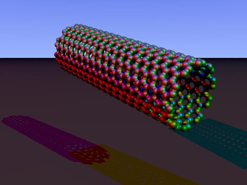
1 Nanostrukturphysik (Nanostructure Physics) Prof. Yong Lei & Dr. Yang Xu Fachgebiet 3D-Nanostrukturierung, Institut für Physik Contact: Office: Unterpoerlitzer Straße 38 (Heisenbergbau) (tel: 3748) Vorlesung: Wedsnesday 9:00 10:30, C 108 Übung: Friday (G), 9:00 10:30, C 110 (a) (b 1 ) (b 2 ) UTAM-prepared free-standing one-dimensional surface nanostructures on Si substrates: Ni nanowire arrays (a) and carbon nanotube arrays (b).
2 Contents of Class 1 A general introduction of fundamentals of nanostructured materials Definition of nanostructures or nano-structured materials Significance of nano-structured materials Structural aspects An outline of all the 10 classes Characterization of nano-strcutures One-dimensional nanostructures Surface Nanostructures realized using UTAM
3 There s plenty of room at the bottom, the principles of physics, as far as I can see, do not speak against the possibility of manoeuvring things atom by atom... By the legendary physicist Richard Feynman in 1959 (Feynman R., Eng Sci, 1960) Progress made in past two decades has proven this statement by the amazing nature of nanomaterials, has achieved exciting technological advancement for the benefit of mankind.
4 Definition of nanostructures or nano-materials The word nanometer has been assigned to indicate the size of 10-9 meter Structures with at least one dimension within nanometer (nm) called nanostructures (Prof. H. Gleiter ) The word nano derived from a Greek word nanos, means dwarf (small) Nanostructures have received high research interest because of their peculiar and fascinating properties, as well as their unique applications superior to their counterparts - bulk materials. Nowadays, nanomaterials and nanostructures are not only one of the hottest fundamental research topics, but also gradually intrude into our daily life.

5 From: J. Henk Introduction to the Theory of Nanostructures (Lecture Notes 2006)
6 Nobel Prizes with research related to nanotechnology: 1986 Physics: G. Binnig, H. Rohrer: design of the scanning tunneling microscope (STM) SPM systems; 1996 Chemistry: R. Curl, H. Kroto, R. Smalley: discovery of fullerenes (C60, bucky balls); 2002 Chemistry: J. Fenn, K. Tanaka, K. Wüthrich: identification and structure analyses of biological macromolecules; 2003 Chemistry: P. Agre, R. MacKinnon: discoveries of channels in cell membranes Physics: A. Geim, K. Novoselov: for groundbreaking experiments regarding the two-dimensional graphene
 Nobel Prize 1986 Physics Designing of the scanning tunneling microscope")

7 Nobel Prizes with research related to nanostructures: G. Binnig (German) & H. Rohrer (Swiss) Nobel Prize 1986 Physics Designing of the scanning tunneling microscope (STM) SPM systems G. Binnig also designed AFM with other 2 scientists, and started the company Definiens in He worked as honorary professors in some universities, e.g., Uni-Muenchen.

8 Konstantin Novoselov & Andre Geim (Russian) Nobel Prize 2010 Physics for groundbreaking experiments regarding the twodimensional graphene 8
9 Prof. Andre Geim (from: en.wikipedia.org/wiki/andre_geim) obtained first tenured position in 1994, associate professor at Uni-Nijmegen, one doctoral student at Nijmegen was Novoselov. Geim said that he had an unpleasant time during his career in Netherlands. He was offered professorships at Nijmegen and Eindhoven, but turned them down as he found the Dutch academic system too hierarchical and full of politicking. "This can be pretty unpleasant at times," he says. "It's not like the British system where every staff member is an equal quantity. Geim writes in his Nobel lecture that "the situation was a bit surreal because outside the university walls I received a warmhearted welcome from everyone around In 2001 he became a professor at the University of Manchester, and was appointed director of the Manchester Centre for Mesoscience and Nanotechnology in 2002.

10 1996: Curl, Kroto, Smalley 1985 or1986: fullerenes (C60, bucky balls); 2010: Geim, Novoselov : 2D graphene The allotropes of carbon: hardest natural substance, diamond one of the softest known substances, graphite. For carbon nanotubes CNT (by Ijima in 1991) and the equally important discovery of inorganic fullerene structures (by Tenne) Allotropes of carbon: a) diamond; b) graphite; c) lonsdaleite; d f) fullerenes (C 60, C 540, C 70 ); g) amorphous carbon; h) carbon nanotube. from
11 Graphene is a 1-atom thick sheet of sp 2 -bonded carbon atoms that are densely packed in a honeycomb crystal lattice. Graphene is easily visualized as an atomic-scale wire made of carbon atoms and their bonds. Graphite consists of many graphene sheets stacked together. (


12 Zigzag carbon nanotube


13 Armchair carbon nanotube
14 Why are nanostructures interesting? small is different: new properties of materials at nanometer scale look at quantum mechanics nanostructure + functions or properties: revolution in information technology, medicine, media...
15 Many opportunities might be realized by making new types of nanostructures (fabrication ways): 1. simply by down-sizing existing microstructures into nm range: most successful example is microelectronics, where smaller means greater performance (since the invention of integrated circuits): more components per chip, faster operation, lower cost, and less power consumption;
16 Structural aspects of nano-structured materials: Extremely large surface area (very large surface/volume ratio): when the dimensions decrease from micron level to nano level, the surface area increases by 3 orders in magnitude. This will lead to much improved and enhanced physical properties (sensing, optical, catalysis...): Cube Cubic structures divided into 8 pieces surface area 2 times(doubled) Cube Cubic structures divided into 1000 pieces surface area 10 times
17 Many opportunities might be realized by making new types of nanostructures (fabrication ways): 2. Miniaturization also represent the trend in a range of other technologies: Information storage, e.g., many efforts to fabricate magnetic and optical storage components with critical dimensions (feature size) as small as tens of nanometer device miniaturization

18 Dual-core CPU feature-size 45 nm From Intel Homepage, Public Relations
19 Electronic properties: Dimensions of a system - comparable with Bohr (exciton) radius (which is comparable to nanowire diameter): energy bands cease to overlap discrete The typical electronic properties of the nanostructures are a result of tunneling currents and coulomb blockade effects. However, owing to their wavelike nature, electrons can tunnel through between two closely adjacent nanostructures If a voltage is applied between two nanostructures, which aligns discrete energy levels, resonant tunneling occurs largely increases tunneling current
20 The physical properties of functional nanostructure are different from those of the bulk materials, especially for optical properties: Quantum confinement effect (size-reduction down to the nm-sized range) a band-gap shift adjust the optical properties of nanostructures. Quantum confinement effect: It is widely accepted that quantum confinement of electrons by the potential wells of nanometer-sized structures provides the most powerful (and versatile) means to control the electrical, optical, magnetic, and thermoelectric properties of a solid-state materials. Metallic nanostructures (especially Au and Ag) have unique optical properties surface-enhanced plasmon resonance light-scattering and Raman scattering (SERS or SRR).
21 Quantum confinement effect When the feature size of a structure (e.g., particle) is comparable with the size of Bohr (exciton) radius (about 2 50nm, usually below nm), electron becomes more confined in particle, quantum confinement effect lead to an increasing of energy band-gap. Furthermore, the valence and conductive bands break into quantized discrete energy levels. Many exceptional physical properties of nano-materials are attributed to the changes in the total energy and structure of the system. Band-gap shift due to the Quantum confinement effect: ΔEg = h2/8r2μ 1.8e2 /4πεoεR

22 Quantum confinement in semiconductor nanoparticles Optical fluorescence of CdSe nanoparticles of various sizes. The band gap emission is observed to shift through the entire visible range, from red emission for the largest particles, to blue emission for the smallest clusters. (B. O. Dabbousi, J. Phys. Chem. B, 1997, 101, 9463)
23 Global funding status in nanotechnology This course is try to overview this 21st century s leading science and technology based on fundamental and applied research during the last 2 decades Nano - World

24 Deutsches Museum Zentralbau des Deutschen Museums
25 Class 1: a general introduction of fundamentals of nanostructured materials, and definition Class 2: research at 3D-Nanostructuring Class 3: optical properties of 1D nanostructures Class 4: carbon nanotubes Class 5: graphene Class 6: 2D atomically thin nanosheets Class 7: lithium-ion batteries: Si nanostructures Class 8: solar water splitting I: fundamentals Class 9: solar water splitting II: nanostructures for water splitting Class 10: solar cells

26 Class 2: research at 3D-Nanostructuring From template to energy: Sodium-ion batteries Solar water splitting Supercapacitors

27 Class 3: optical properties of 1D nanostructures Features Quantum confinement Nanowire lasing Field emission display

28 Class 4: carbon nanotubes History Fabrication Applications
29 Class 5: graphene Introduction Brief history Characterizing graphene flakes Devices with peeled graphene Alternatives to mechanical exfoliation

30 Class 6: atomically thin nanosheets Characterization of structure Electronic structure regulation Energy device construction

31 Class 7: nanostructured Si anodes for lithium-ion batteries Principle of lithiumion batteries Opportunities and challenges of Si anodes Nanostructured Si anodes

32 Class 8: fundamentals of solar water splitting Related semiconductor physics Thermodynamic and kinetics of semiconductor-liquid interface

33 Class 9: nanostructures for solar water splitting Pros and cons Material designs and nanostrcutured architectures Cathode Electrolyte Anode


34 Class 10: nanostructures for enhancing light absorption in solar cells Semiconductor nanostructures Metal nanostructures: surface plasmons
35 Characterization of nano-strcutures An appropriate characterization will play a crucial role in determining various structures and properties of nanostructures. Three broadly approved aspects of characterization are 1. Morphology 2. Crystalline structure 3. Chemical analysis
36 SEM: Scanning Electron Microscopy; STM/AFM: Scanning Tunneling Microscopy/Atomic Force Microscopy; ATEM: Analytical Transmission Electron Microscopy X-Ray: X-ray Morphology; IP: Image Processing; LM: Lightweight Morphology; RBS: Rutherford Backscattering Spectrometry (Kelsall et al., Nanoscale science and technology. 2005)
37 ATEM: Analytical Transmission Electron Microscopy; AES: Auger Electron Spectrometer; XRD: X-ray Diffraction; RBS: Rutherford Backscattering Spectrometry; XPS: X-ray Photoelectron Spectrometer; (Kelsall et al., Nanoscale science and technology. 2005)
38 SEM: Scanning Electron Microscopy; ATEM: Analytical Transmission Electron Microscopy; AEM: Auger Electron Microscopy. XRD: X-ray Diffraction; LEED: Lowenergy electron diffraction; RBS: Rutherford Backscattering Spectrometry (Kelsall et al., Nanoscale science and technology. 2005)


39 Types of Nanostructure: Two-dimensional nanostructure: nanowalls, quantum wells... One-dimensional nanostructure: nanowires, nanotubes, nanorods, nanobelts... Zero-dimensional nanostructure: quantum dots or nanoparticles

40 Graphene is a 1-atom thick sheets of sp 2 -bonded carbon atoms that are densely packed in a honeycomb crystal lattice. Graphene is easily visualized as an atomicscale wire made of carbon atoms and their bonds. Graphite consists of many graphene sheets stacked together. (


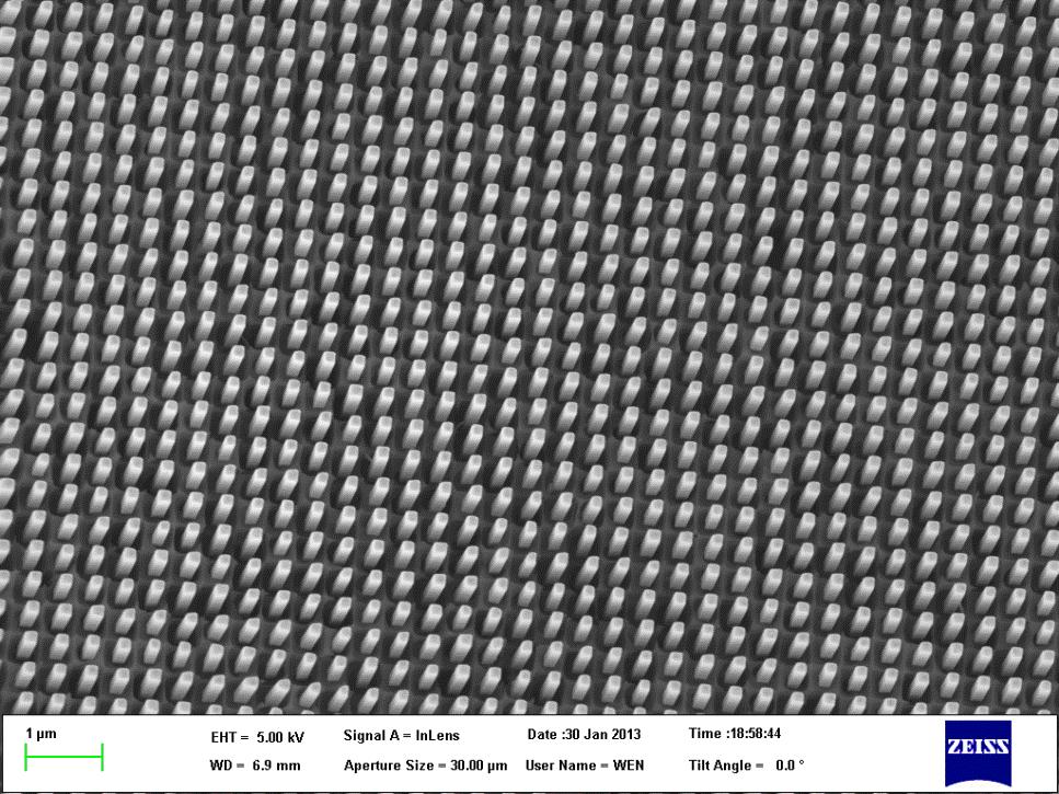
41 Templates with large-scale (1 mm 2 ) perfect rectangular pore arrays without defect

42 Templates with large-scale (1 mm 2 ) perfect rectangular pore arrays without defect


43 Perfect regular 3D nanostructure arrays with different wire configuration
44 One dimensional nanostructures One dimensional (1D) nanostructure: nanowires, nanotubes, nanorods, nanobelts... One dimensional nanostructure refers to the systems with the lateral dimension in the range of nm. In comparison with 0D nanostructures, 1D nanostructures provides a better model system to investigate the dependence of properties (electronic transport, optical, and mechanical) on size confinement and dimension. Nanowires, in particular, plays an important role as both interconnects and active components in preparing nanoscale devices (Nano-devices).
45 One-Dimensional Nanostructures (a) (b 1 ) (b 2 ) UTAM-prepared free-standing one-dimensional surface nanostructures on Si substrates: Ni nanowire arrays (a) and carbon nanotube arrays (b). (Y. Lei et al., Chemistry of Materials, 2004)
 nanobelts/nanoribbons; (F) nanotapes; (G) dendrites; (H) hierarchical nanostructures; (I) nanosphere assembly; (J) nanosprings. (Kolmakov et al.")
46 A schematic summary of the kinds of one dimensional nanostructures already reported: (A) nanowires and nanorods; (B) core shell structures; (C) nanotubes/hollow nanorods; (D) heterostructures; (E) nanobelts/nanoribbons; (F) nanotapes; (G) dendrites; (H) hierarchical nanostructures; (I) nanosphere assembly; (J) nanosprings. (Kolmakov et al., Annu Rev Mater Res 2004)
47 CdS replicated mask Alumina CdS nanodots Highly ordered CdS nanodot arrays, UTAMs and CdS top layer on the surface of the UTAM.


48 Surface patterns in nature Structural color function of surface patterns butterfly 1 µm peacock packing of melanin cylinders (provided by L Chi)
49 Surface patterns and structures (artificial) and their applications in diverse (micro-electronic) devices Dual-core CPU feature-size 45 nm From Intel Homepage, Public Relations
50 Surface Nano-Patterning Fabrication of surface nanostructures Memory devices with high integration density; Field emission devices; Sensors with high sensitivity; Optical devices with tunable properties What is an excellent surface nano-patterning technique? 1. Ability to prepare surface patterns within the nanosized range; 2. Well-defined surface nano-patterns; 3. Large pattern area high throughput; 4. A general process applicable; 5. Low cost. Perfect?
51 Some surface nano-patterning techniques in fabricating ordered surface nanostructures Electron-beam lithography Excellent structural controlling Low throughput High equipment costs Imprint technologies High throughput Wear Structures with low aspect ratio Self assembly Low costs High throughput Limited class of materials Low structural controlling Alternative method that combines these advantages and is applicable for a broad range of surface nanostructures? UTAM (ultra-thin alumina mask) surface nano-patterning: Template-based surface nano-fabrications

 Configuration diagram of")
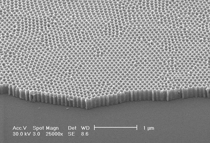
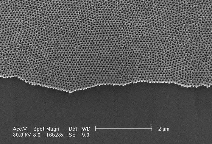
52 Porous Alumina Membranes (PAMs) Interesting and useful features: highly ordered pore arrays + large area Nanometer-sized pores High aspect ratio size controllable ( nm) Configuration diagram of the PAMs
 and 3-4 μm (b), respectively.")
53 Porous Alumina Membranes (PAMs) (a) (b) Regular arrays of short (a) and long Ni nanowires (b) after the removal of PAM, the diameter is about 90 nm, the length is about nm (a) and 3-4 μm (b), respectively. thus the aspect ratio of the nanowires are about 10 (a) and 40 (b), respectively.
54 UTAM surface nano-patterning technique Fabrication of Highly Ordered Nanoparticle Arrays Using Ultra-thin Alumina Mask (UTAM) Motivation Use ultra-thin ordered porous alumina as evaporation or etching masks, and transfer the regularity of the pore arrays to the nanostructure arrays on substrates.
55 Fabrication process Fabricating ultra-thin alumina masks (UTAM) on Al foils and then mounting them onto the surface of silicon wafers First alumina layer Al Si foil wafer Ultra-thin Second alumina layer mask
56
57 Fabrication of the nanodot arrays Si wafer Ultra-thin Nanoparticle alumina array mask

58 CdS replicated mask Alumina CdS nanodots Highly ordered CdS nanodot arrays, UTAMs and CdS top layer on the surface of the UTAM.
59 Class 1: a general introduction of fundamentals of nanostructured materials, and definition Class 2: research at 3D-Nanostructuring Class 3: optical properties of 1D nanostructures Class 4: carbon nanotubes Class 5: graphene Class 6: 2D atomically thin nanosheets Class 7: lithium-ion batteries: Si nanostructures Class 8: solar water splitting I: fundamentals Class 9: solar water splitting II: nanostructures for water splitting Class 10: solar cells
60 Thanks for your attention
Nanostrukturphysik (Nanostructure Physics)
") Nanostrukturphysik (Nanostructure Physics) Prof. Yong Lei & Dr. Huaping Zhao Fachgebiet Angewandte Nanophysik, Institut für Physik Contact: yong.lei@tu-ilmenau.de; huaping.zhao@tu-ilmenau.de Office: Unterpoerlitzer
Nanostrukturphysik (Nanostructure Physics) Prof. Yong Lei & Dr. Huaping Zhao Fachgebiet Angewandte Nanophysik, Institut für Physik Contact: yong.lei@tu-ilmenau.de; huaping.zhao@tu-ilmenau.de Office: Unterpoerlitzer
Nanostrukturphysik (Nanostructure Physics)
") Nanostrukturphysik (Nanostructure Physics) Yong Lei & Fabian Grote Fachgebiet 3D-Nanostrukturierung, Institut für Physik Contact: yong.lei@tu-ilmenau.de; fabian.grote@tu-ilmenau.de Office: Heliosbau 1102,
Nanostrukturphysik (Nanostructure Physics) Yong Lei & Fabian Grote Fachgebiet 3D-Nanostrukturierung, Institut für Physik Contact: yong.lei@tu-ilmenau.de; fabian.grote@tu-ilmenau.de Office: Heliosbau 1102,
Techniken der Oberflächenphysik (Technique of Surface Physics)
") Techniken der Oberflächenphysik (Technique of Surface Physics) Yong Lei & Fabian Grote Fachgebiet 3D-Nanostrukturierung, Institut für Physik Contact: yong.lei@tu-ilmenau.de; fabian.grote@tu-ilmenau.de
Techniken der Oberflächenphysik (Technique of Surface Physics) Yong Lei & Fabian Grote Fachgebiet 3D-Nanostrukturierung, Institut für Physik Contact: yong.lei@tu-ilmenau.de; fabian.grote@tu-ilmenau.de
Techniken der Oberflächenphysik (Techniques of Surface Physics)
") Techniken der Oberflächenphysik (Techniques of Surface Physics) Prof. Yong Lei & Dr. Yang Xu, Dr. Huaping Zhao Fachgebiet Angewante Nanophysik, Institut für Physik Contact: yong.lei@tu-ilmenau.de yang.xu@tu-ilmenau.de
Techniken der Oberflächenphysik (Techniques of Surface Physics) Prof. Yong Lei & Dr. Yang Xu, Dr. Huaping Zhao Fachgebiet Angewante Nanophysik, Institut für Physik Contact: yong.lei@tu-ilmenau.de yang.xu@tu-ilmenau.de
Nanostrukturphysik (Nanostructure Physics)
") Nanostrukturphysik (Nanostructure Physics) Prof. Yong Lei & Dr. Yang Xu Fachgebiet 3D-Nanostrukturierung, Institut für Physik Contact: yong.lei@tu-ilmenau.de; yang.xu@tu-ilmenau.de Office: Unterpoerlitzer
Nanostrukturphysik (Nanostructure Physics) Prof. Yong Lei & Dr. Yang Xu Fachgebiet 3D-Nanostrukturierung, Institut für Physik Contact: yong.lei@tu-ilmenau.de; yang.xu@tu-ilmenau.de Office: Unterpoerlitzer
Techniken der Oberflächenphysik (Techniques of Surface Physics)
") Techniken der Oberflächenphysik (Techniques of Surface Physics) Prof. Yong Lei & Dr. Yang Xu Fachgebiet 3D-Nanostrukturierung, Institut für Physik Contact: yong.lei@tu-ilmenau.de yang.xu@tu-ilmenau.de
Techniken der Oberflächenphysik (Techniques of Surface Physics) Prof. Yong Lei & Dr. Yang Xu Fachgebiet 3D-Nanostrukturierung, Institut für Physik Contact: yong.lei@tu-ilmenau.de yang.xu@tu-ilmenau.de
Halbleiter Prof. Yong Lei Prof. Thomas Hannappel
 Halbleiter Prof. Yong Lei Prof. Thomas Hannappel yong.lei@tu-ilmenau.de thomas.hannappel@tu-ilmenau.de http:///nanostruk/ Organic semiconductors Small-molecular materials Rubrene Pentacene Polymers PEDOT:PSS
Nanotechnology. Yung Liou P601 Institute of Physics Academia Sinica
 Nanotechnology Yung Liou P601 yung@phys.sinica.edu.tw Institute of Physics Academia Sinica 1 1st week Definition of Nanotechnology The Interagency Subcommittee on Nanoscale Science, Engineering and Technology
Nanostrukturphysik (Nanostructure Physics)
") Nanostrukturphysik (Nanostructure Physics) Prof. Yong Lei & Dr. Yang Xu Fachgebiet 3D-Nanostrukturierung, Institut für Physik Contact: yong.lei@tu-ilmenau.de; yang.xu@tu-ilmenau.de Office: Unterpoerlitzer
Nanostrukturphysik (Nanostructure Physics) Prof. Yong Lei & Dr. Yang Xu Fachgebiet 3D-Nanostrukturierung, Institut für Physik Contact: yong.lei@tu-ilmenau.de; yang.xu@tu-ilmenau.de Office: Unterpoerlitzer
Chapter 10. Nanometrology. Oxford University Press All rights reserved.
 Chapter 10 Nanometrology Oxford University Press 2013. All rights reserved. 1 Introduction Nanometrology is the science of measurement at the nanoscale level. Figure illustrates where nanoscale stands
Techniken der Oberflächenphysik (Techniques of Surface Physics)
") Techniken der Oberflächenphysik (Techniques of Surface Physics) Prof. Yong Lei Dr. Ynag Xu and Mr. Grote Fabian Fachgebiet 3D-Nanostrukturierung, Institut für Physik Contact: yong.lei@tu-ilmenau.de; yang.xu@tu-ilmenau.de
Techniken der Oberflächenphysik (Techniques of Surface Physics) Prof. Yong Lei Dr. Ynag Xu and Mr. Grote Fabian Fachgebiet 3D-Nanostrukturierung, Institut für Physik Contact: yong.lei@tu-ilmenau.de; yang.xu@tu-ilmenau.de
Seminars in Nanosystems - I
 Seminars in Nanosystems - I Winter Semester 2011/2012 Dr. Emanuela Margapoti Emanuela.Margapoti@wsi.tum.de Dr. Gregor Koblmüller Gregor.Koblmueller@wsi.tum.de Seminar Room at ZNN 1 floor Topics of the
Nanostrukturphysik Übung 2 (Class 3&4)
") Nanostrukturphysik Übung 2 (Class 3&4) Prof. Yong Lei & Dr. Yang Xu 2017.05.03 Fachgebiet 3D-Nanostrukturierung, Institut für Physik Contact: yong.lei@tu-ilmenau.de (3748), yang.xu@tuilmenau.de (4902)
Nanostrukturphysik Übung 2 (Class 3&4) Prof. Yong Lei & Dr. Yang Xu 2017.05.03 Fachgebiet 3D-Nanostrukturierung, Institut für Physik Contact: yong.lei@tu-ilmenau.de (3748), yang.xu@tuilmenau.de (4902)
Graphene. Tianyu Ye November 30th, 2011
 Graphene Tianyu Ye November 30th, 2011 Outline What is graphene? How to make graphene? (Exfoliation, Epitaxial, CVD) Is it graphene? (Identification methods) Transport properties; Other properties; Applications;
Nanotechnology Fabrication Methods.
 Nanotechnology Fabrication Methods. 10 / 05 / 2016 1 Summary: 1.Introduction to Nanotechnology:...3 2.Nanotechnology Fabrication Methods:...5 2.1.Top-down Methods:...7 2.2.Bottom-up Methods:...16 3.Conclusions:...19
Materials. Definitions of nanotechnology. The term nanotechnology was invented by Professor Norio Taniguchi at the University of Tokyo in 1971.
 Materials Definitions of nanotechnology The term nanotechnology was invented by Professor Norio Taniguchi at the University of Tokyo in 1971. The original definition, translated into English Nano-technology'
Chapter 1 Introduction
 Chapter 1 Introduction A nanometer (nm) is one billionth (10-9 ) of a meter. Nanoscience can be defined as the science of objects and phenomena occurring at the scale of 1 to 100 nm. The range of 1 100
Chapter 12. Nanometrology. Oxford University Press All rights reserved.
 Chapter 12 Nanometrology Introduction Nanometrology is the science of measurement at the nanoscale level. Figure illustrates where nanoscale stands in relation to a meter and sub divisions of meter. Nanometrology
Nanostructures. Lecture 13 OUTLINE
 Nanostructures MTX9100 Nanomaterials Lecture 13 OUTLINE -What is quantum confinement? - How can zero-dimensional materials be used? -What are one dimensional structures? -Why does graphene attract so much
Carbon based Nanoscale Electronics
 Carbon based Nanoscale Electronics 09 02 200802 2008 ME class Outline driving force for the carbon nanomaterial electronic properties of fullerene exploration of electronic carbon nanotube gold rush of
EN2912C: Future Directions in Computing Lecture 08: Overview of Near-Term Emerging Computing Technologies
 EN2912C: Future Directions in Computing Lecture 08: Overview of Near-Term Emerging Computing Technologies Prof. Sherief Reda Division of Engineering Brown University Fall 2008 1 Near-term emerging computing
Nanostrukturphysik. Prof. Yong Lei & Dr. Yang Xu Fachgebiet 3D-Nanostrukturierung, Institut für Physik
 Nanostrukturphysik Prof. Yong Lei & Dr. Yang Xu Fachgebiet 3D-Nanostrukturierung, Institut für Physik Contact: yong.lei@tu-ilmenau.de (3748), yang.xu@tuilmenau.de (4902) Office: Gebäude V202, Unterpörlitzer
Nanomaterials and their Optical Applications
 Nanomaterials and their Optical Applications Winter Semester 2013 Lecture 02 rachel.grange@uni-jena.de http://www.iap.uni-jena.de/multiphoton Lecture 2: outline 2 Introduction to Nanophotonics Theoretical
In the name of Allah
 In the name of Allah Nano chemistry- 4 th stage Lecture No. 1 History of nanotechnology 16-10-2016 Assistance prof. Dr. Luma Majeed Ahmed lumamajeed2013@gmail.com, luma.ahmed@uokerbala.edu.iq Nano chemistry-4
From nanophysics research labs to cell phones. Dr. András Halbritter Department of Physics associate professor
 From nanophysics research labs to cell phones Dr. András Halbritter Department of Physics associate professor Curriculum Vitae Birth: 1976. High-school graduation: 1994. Master degree: 1999. PhD: 2003.
In today s lecture, we will cover:
 In today s lecture, we will cover: Metal and Metal oxide Nanoparticles Semiconductor Nanocrystals Carbon Nanotubes 1 Week 2: Nanoparticles Goals for this section Develop an understanding of the physical
1.1. Introduction to Nanoscience and Nanotechnology
 1.1. Introduction to Nanoscience and Nanotechnology 1.1.1. A Brief Historical Overview Before trying to understand and discuss about synthesis, characterization and application of nanomaterials, it is
There's Plenty of Room at the Bottom
 There's Plenty of Room at the Bottom 12/29/1959 Feynman asked why not put the entire Encyclopedia Britannica (24 volumes) on a pin head (requires atomic scale recording). He proposed to use electron microscope
The many forms of carbon
 The many forms of carbon Carbon is not only the basis of life, it also provides an enormous variety of structures for nanotechnology. This versatility is connected to the ability of carbon to form two
29: Nanotechnology. What is Nanotechnology? Properties Control and Understanding. Nanomaterials
 29: Nanotechnology What is Nanotechnology? Properties Control and Understanding Nanomaterials Making nanomaterials Seeing at the nanoscale Quantum Dots Carbon Nanotubes Biology at the Nanoscale Some Applications
Nanostructure. Materials Growth Characterization Fabrication. More see Waser, chapter 2
 Nanostructure Materials Growth Characterization Fabrication More see Waser, chapter 2 Materials growth - deposition deposition gas solid Physical Vapor Deposition Chemical Vapor Deposition Physical Vapor
Halbleiter. Prof. Yong Lei. Prof. Thomas Hannappel.
 Halbleiter Prof. Yong Lei Prof. Thomas Hannappel yong.lei@tu-ilemnau.de thomas.hannappel@tu-ilmenau.de Important Events in Semiconductors History 1833 Michael Faraday discovered temperature-dependent conductivity
Overview. Carbon in all its forms. Background & Discovery Fabrication. Important properties. Summary & References. Overview of current research
 Graphene Prepared for Solid State Physics II Pr Dagotto Spring 2009 Laurene Tetard 03/23/09 Overview Carbon in all its forms Background & Discovery Fabrication Important properties Overview of current
Solutions for Assignment-8
 Solutions for Assignment-8 Q1. The process of adding impurities to a pure semiconductor is called: [1] (a) Mixing (b) Doping (c) Diffusing (d) None of the above In semiconductor production, doping intentionally
3-month progress Report
 3-month progress Report Graphene Devices and Circuits Supervisor Dr. P.A Childs Table of Content Abstract... 1 1. Introduction... 1 1.1 Graphene gold rush... 1 1.2 Properties of graphene... 3 1.3 Semiconductor
General concept and defining characteristics of AFM. Dina Kudasheva Advisor: Prof. Mary K. Cowman
 General concept and defining characteristics of AFM Dina Kudasheva Advisor: Prof. Mary K. Cowman Overview Introduction History of the SPM invention Technical Capabilities Principles of operation Examples
Carbon nanomaterials. Gavin Lawes Wayne State University.
 Carbon nanomaterials Gavin Lawes Wayne State University glawes@wayne.edu Outline 1. Carbon structures 2. Carbon nanostructures 3. Potential applications for Carbon nanostructures Periodic table from bpc.edu
Techniken der Oberflächenphysik (Techniques of Surface Physics)
") Techniken der Oberflächenphysik (Techniques of Surface Physics) Prof. Yong Lei & Dr. Yang Xu (& Liying Liang) Fachgebiet 3D-Nanostrukturierung, Institut für Physik Contact: yong.lei@tu-ilmenau.de; yang.xu@tu-ilmenau.de;
Techniken der Oberflächenphysik (Techniques of Surface Physics) Prof. Yong Lei & Dr. Yang Xu (& Liying Liang) Fachgebiet 3D-Nanostrukturierung, Institut für Physik Contact: yong.lei@tu-ilmenau.de; yang.xu@tu-ilmenau.de;
CHAPTER 11 Semiconductor Theory and Devices
 CHAPTER 11 Semiconductor Theory and Devices 11.1 Band Theory of Solids 11.2 Semiconductor Theory 11.3 Semiconductor Devices 11.4 Nanotechnology It is evident that many years of research by a great many
materials, devices and systems through manipulation of matter at nanometer scale and exploitation of novel phenomena which arise because of the
 Nanotechnology is the creation of USEFUL/FUNCTIONAL materials, devices and systems through manipulation of matter at nanometer scale and exploitation of novel phenomena which arise because of the nanometer
Nanoelectronics. Topics
 Nanoelectronics Topics Moore s Law Inorganic nanoelectronic devices Resonant tunneling Quantum dots Single electron transistors Motivation for molecular electronics The review article Overview of Nanoelectronic
Electrical and Optical Properties. H.Hofmann
 Introduction to Nanomaterials Electrical and Optical Properties H.Hofmann Electrical Properties Ohm: G= σw/l where is the length of the conductor, measured in meters [m], A is the cross-section area of
Physics and Material Science of Semiconductor Nanostructures
 Physics and Material Science of Semiconductor Nanostructures PHYS 570P Prof. Oana Malis Email: omalis@purdue.edu Course website: http://www.physics.purdue.edu/academic_programs/courses/phys570p/ 1 Course
CHARACTERIZATION of NANOMATERIALS KHP
 CHARACTERIZATION of NANOMATERIALS Overview of the most common nanocharacterization techniques MAIN CHARACTERIZATION TECHNIQUES: 1.Transmission Electron Microscope (TEM) 2. Scanning Electron Microscope
MS482 Materials Characterization ( 재료분석 ) Lecture Note 11: Scanning Probe Microscopy. Byungha Shin Dept. of MSE, KAIST
 Lecture Note 11: Scanning Probe Microscopy. Byungha Shin Dept. of MSE, KAIST") 2015 Fall Semester MS482 Materials Characterization ( 재료분석 ) Lecture Note 11: Scanning Probe Microscopy Byungha Shin Dept. of MSE, KAIST 1 Course Information Syllabus 1. Overview of various characterization
2015 Fall Semester MS482 Materials Characterization ( 재료분석 ) Lecture Note 11: Scanning Probe Microscopy Byungha Shin Dept. of MSE, KAIST 1 Course Information Syllabus 1. Overview of various characterization
Nano Materials and Devices
 Nano Materials and Devices Professor Michael Austin Platform Technologies Research Institute Nano Materials and Devices Program Aim: to develop an integrated capability in nanotechnology Design and modelling
There s plenty of room at the bottom! - R.P. Feynman, Nanostructure: a piece of material with at least one dimension less than 100 nm in extent.
 Nanostructures and Nanotechnology There s plenty of room at the bottom! - R.P. Feynman, 1959 Materials behave differently when structured at the nm scale than they do in bulk. Technologies now exist that
PHYS 3313 Section 001 Lecture #21 Monday, Nov. 26, 2012
 PHYS 3313 Section 001 Lecture #21 Monday, Nov. 26, 2012 Superconductivity Theory, The Cooper Pair Application of Superconductivity Semi-Conductor Nano-technology Graphene 1 Announcements Your presentations
Electrochemically Synthesized Multi-block
 Electrochemically Synthesized Multi-block Nanorods Sungho Park SungKyunKwan University, Department of Chemistry & SKKU Advanced Institute of Nanotechnology (SAINT) J. Am. Chem. Soc. 2003, 125, 2282-2290
Graphene Fundamentals and Emergent Applications
 Graphene Fundamentals and Emergent Applications Jamie H. Warner Department of Materials University of Oxford Oxford, UK Franziska Schaffel Department of Materials University of Oxford Oxford, UK Alicja
Fabrication at the nanoscale for nanophotonics
 Fabrication at the nanoscale for nanophotonics Ilya Sychugov, KTH Materials Physics, Kista silicon nanocrystal by electron beam induced deposition lithography Outline of basic nanofabrication methods Devices
MS482 Materials Characterization ( 재료분석 ) Lecture Note 2: UPS
 Lecture Note 2: UPS") 2016 Fall Semester MS482 Materials Characterization ( 재료분석 ) Lecture Note 2: UPS Byungha Shin Dept. of MSE, KAIST 1 Course Information Syllabus 1. Overview of various characterization techniques (1 lecture)
2016 Fall Semester MS482 Materials Characterization ( 재료분석 ) Lecture Note 2: UPS Byungha Shin Dept. of MSE, KAIST 1 Course Information Syllabus 1. Overview of various characterization techniques (1 lecture)
ESH Benign Processes for he Integration of Quantum Dots (QDs)
") ESH Benign Processes for he Integration of Quantum Dots (QDs) PIs: Karen K. Gleason, Department of Chemical Engineering, MIT Graduate Students: Chia-Hua Lee: PhD Candidate, Department of Material Science
ESH Benign Processes for he Integration of Quantum Dots (QDs) PIs: Karen K. Gleason, Department of Chemical Engineering, MIT Graduate Students: Chia-Hua Lee: PhD Candidate, Department of Material Science
CSCI 2570 Introduction to Nanocomputing
 CSCI 2570 Introduction to Nanocomputing The Emergence of Nanotechnology John E Savage Purpose of the Course The end of Moore s Law is in sight. Researchers are now exploring replacements for standard methods
1.0 Introduction. 1.1 Nanotechnology Historical Developments
 1.0 Introduction 1.1 Nanotechnology Historical Developments Around 370BC, Democritus a Greek philosopher developed the atomic theory of matter. Nano in GREEK means DWARF. The prefix nano means a billionth
Crystalline Surfaces for Laser Metrology
 Crystalline Surfaces for Laser Metrology A.V. Latyshev, Institute of Semiconductor Physics SB RAS, Novosibirsk, Russia Abstract: The number of methodological recommendations has been pronounced to describe
Scripts for High School Visits to the Herman Group at Columbia University
 Scripts for High School Visits to the Herman Group at Columbia University Evan Spotte-Smith, Jiayang Hu, and Irving P. Herman April, 2017; updated June, 2017 These presentations were developed for visits
Graphene films on silicon carbide (SiC) wafers supplied by Nitride Crystals, Inc.
 wafers supplied by Nitride Crystals, Inc.") 9702 Gayton Road, Suite 320, Richmond, VA 23238, USA Phone: +1 (804) 709-6696 info@nitride-crystals.com www.nitride-crystals.com Graphene films on silicon carbide (SiC) wafers supplied by Nitride Crystals,
9702 Gayton Road, Suite 320, Richmond, VA 23238, USA Phone: +1 (804) 709-6696 info@nitride-crystals.com www.nitride-crystals.com Graphene films on silicon carbide (SiC) wafers supplied by Nitride Crystals,
EE 527 MICROFABRICATION. Lecture 5 Tai-Chang Chen University of Washington
 EE 527 MICROFABRICATION Lecture 5 Tai-Chang Chen University of Washington MICROSCOPY AND VISUALIZATION Electron microscope, transmission electron microscope Resolution: atomic imaging Use: lattice spacing.
Nanoscale Surface Physics PHY 5XXX
 SYLLABUS Nanoscale Surface Physics PHY 5XXX Spring Semester, 2006 Instructor: Dr. Beatriz Roldán-Cuenya Time: Tuesday and Thursday 4:00 to 5:45 pm Location: Theory: MAP 306, Laboratory: MAP 148 Office
Wafer-scale fabrication of graphene
 Wafer-scale fabrication of graphene Sten Vollebregt, MSc Delft University of Technology, Delft Institute of Mircosystems and Nanotechnology Delft University of Technology Challenge the future Delft University
Welcome to NANO* 2000
 Lecture Zero Welcome to NANO* 2000 First - the "big picture" of the course and the course outline -grading scheme - exam schedule - review paper - lab (Jay) last revision September 4 2013: MDB 0-1 NANO*
Nanomaterials and their Optical Applications
 Nanomaterials and their Optical Applications Winter Semester 2012 Lecture 04 rachel.grange@uni-jena.de http://www.iap.uni-jena.de/multiphoton Lecture 4: outline 2 Characterization of nanomaterials SEM,
Nanotechnology? Source: National Science Foundation (NSF), USA
, USA") 2 2 Nanotechnology? Ability to work at the atomic, molecular and even sub-molecular levels in order to create and use material structures, devices and systems with new properties and functions Source:
2 2 Nanotechnology? Ability to work at the atomic, molecular and even sub-molecular levels in order to create and use material structures, devices and systems with new properties and functions Source:
Nanotechnology. Gavin Lawes Department of Physics and Astronomy
 Nanotechnology Gavin Lawes Department of Physics and Astronomy Earth-Moon distance 4x10 8 m (courtesy NASA) Length scales (Part I) Person 2m Magnetic nanoparticle 5x10⁻⁹ m 10 10 m 10 5 m 1 m 10-5 m 10-10
TRANSVERSE SPIN TRANSPORT IN GRAPHENE
 International Journal of Modern Physics B Vol. 23, Nos. 12 & 13 (2009) 2641 2646 World Scientific Publishing Company TRANSVERSE SPIN TRANSPORT IN GRAPHENE TARIQ M. G. MOHIUDDIN, A. A. ZHUKOV, D. C. ELIAS,
Nanotechnology where size matters
 Nanotechnology where size matters J Emyr Macdonald Overview Ways of seeing very small things What is nanotechnology and why is it important? Building nanostructures What we can do with nanotechnology?
Lectures Graphene and
 Lectures 15-16 Graphene and carbon nanotubes Graphene is atomically thin crystal of carbon which is stronger than steel but flexible, is transparent for light, and conducts electricity (gapless semiconductor).
MS482 Materials Characterization ( 재료분석 ) Lecture Note 5: RBS
 Lecture Note 5: RBS") 2016 Fall Semester MS482 Materials Characterization ( 재료분석 ) Lecture Note 5: RBS Byungha Shin Dept. of MSE, KAIST 1 Course Information Syllabus 1. Overview of various characterization techniques (1 lecture)
2016 Fall Semester MS482 Materials Characterization ( 재료분석 ) Lecture Note 5: RBS Byungha Shin Dept. of MSE, KAIST 1 Course Information Syllabus 1. Overview of various characterization techniques (1 lecture)
Carbon Structure Simulations using Crystal Viewer Tool
 Carbon Structure Simulations using Crystal Viewer Tool The Crystal Viewer tool in nanohub.org can be used to build three carbon nanostructures: graphene sheets, Buckminsterfullerene, Bucky balls (C 60
Quantum Dots for Advanced Research and Devices
 Quantum Dots for Advanced Research and Devices spectral region from 450 to 630 nm Zero-D Perovskite Emit light at 520 nm ABOUT QUANTUM SOLUTIONS QUANTUM SOLUTIONS company is an expert in the synthesis
Ecole Franco-Roumaine : Magnétisme des systèmes nanoscopiques et structures hybrides - Brasov, Modern Analytical Microscopic Tools
 1. Introduction Solid Surfaces Analysis Group, Institute of Physics, Chemnitz University of Technology, Germany 2. Limitations of Conventional Optical Microscopy 3. Electron Microscopies Transmission Electron
Surface atoms/molecules of a material act as an interface to its surrounding environment;
 1 Chapter 1 Thesis Overview Surface atoms/molecules of a material act as an interface to its surrounding environment; their properties are often complicated by external adsorbates/species on the surface
ME 4875/MTE C16. Introduction to Nanomaterials and Nanotechnology. Lecture 2 - Applications of Nanomaterials + Projects
 ME 4875/MTE 575 - C16 Introduction to Nanomaterials and Nanotechnology Lecture 2 - Applications of Nanomaterials + Projects 1 Project Teams of 4 students each Literature review of one application of nanotechnology
Special Topics in Semiconductor Nanotechnology ECE 598XL
 Special Topics in Semiconductor Nanotechnology ECE 598XL Fall 2009 ECE 598XL Syllabus Overview: size matters Formation Process Characterization SOA device applications and potentials Homework or quizzes
Like space travel and the Internet before it, the possibilities of the nano world catches the imagination of school children and scientists alike.
 The Nano World Preface Nano is the cool thing and it s the buzzword Like space travel and the Internet before it, the possibilities of the nano world catches the imagination of school children and scientists
Raman spectroscopy at the edges of multilayer graphene
 Raman spectroscopy at the edges of multilayer graphene Q. -Q. Li, X. Zhang, W. -P. Han, Y. Lu, W. Shi, J. -B. Wu, P. -H. Tan* State Key Laboratory of Superlattices and Microstructures, Institute of Semiconductors,
554 Chapter 10 Liquids and Solids
 554 Chapter 10 Liquids and Solids above 7376 kpa, CO 2 is a supercritical fluid, with properties of both gas and liquid. Like a gas, it penetrates deep into the coffee beans; like a liquid, it effectively
Initial Stages of Growth of Organic Semiconductors on Graphene
 Initial Stages of Growth of Organic Semiconductors on Graphene Presented by: Manisha Chhikara Supervisor: Prof. Dr. Gvido Bratina University of Nova Gorica Outline Introduction to Graphene Fabrication
NANOSCIENCE AND NANOTECHNOLOGY
 NANOSCIENCE AND NANOTECHNOLOGY Yuehe Lin WHAT IS NANOTECHNOLOGY Nanotechnology is the understanding and control of matter at dimensions of roughly 1 to 100 nanometers, where unique phenomena enable novel
Molecular Electronics For Fun and Profit(?)
") Molecular Electronics For Fun and Profit(?) Prof. Geoffrey Hutchison Department of Chemistry University of Pittsburgh geoffh@pitt.edu July 22, 2009 http://hutchison.chem.pitt.edu Moore s Law: Transistor
Molecular Electronics For Fun and Profit(?) Prof. Geoffrey Hutchison Department of Chemistry University of Pittsburgh geoffh@pitt.edu July 22, 2009 http://hutchison.chem.pitt.edu Moore s Law: Transistor
Title of file for HTML: Supplementary Information Description: Supplementary Figures and Supplementary References
 Title of file for HTML: Supplementary Information Description: Supplementary Figures and Supplementary References Supplementary Figure 1. SEM images of perovskite single-crystal patterned thin film with
Nanophysics: Main trends
 Nano-opto-electronics Nanophysics: Main trends Nanomechanics Main issues Light interaction with small structures Molecules Nanoparticles (semiconductor and metallic) Microparticles Photonic crystals Nanoplasmonics
Introduction to Nanotechnology Chapter 5 Carbon Nanostructures Lecture 1
 Introduction to Nanotechnology Chapter 5 Carbon Nanostructures Lecture 1 ChiiDong Chen Institute of Physics, Academia Sinica chiidong@phys.sinica.edu.tw 02 27896766 Carbon contains 6 electrons: (1s) 2,
Course file PPY15204 Nanoscience and Nanomaterials Table of Contents
 Department Physics Nanotechnology : M.sc Physics Course file PPY15204 Table Contents Second Year MSc Physics (2015-2016 Regulation) Detailed Lesson Plan UNIT-I: INTRODUCTION TO NANOTECHNOLOGY History Importance
Nanotechnology Nanofabrication of Functional Materials. Marin Alexe Max Planck Institute of Microstructure Physics, Halle - Germany
 Nanotechnology Nanofabrication of Functional Materials Marin Alexe Max Planck Institute of Microstructure Physics, Halle - Germany Contents Part I History and background to nanotechnology Nanoworld Nanoelectronics
NANOSCIENCE: TECHNOLOGY AND ADVANCED MATERIALS
 UNIVERSITY OF SOUTHAMPTON PHYS6014W1 SEMESTER 2 EXAMINATIONS 2012-2013 NANOSCIENCE: TECHNOLOGY AND ADVANCED MATERIALS DURATION 120 MINS (2 Hours) This paper contains 8 questions Answer ALL questions in
Scanning Probe Microscopy. Amanda MacMillan, Emmy Gebremichael, & John Shamblin Chem 243: Instrumental Analysis Dr. Robert Corn March 10, 2010
 Scanning Probe Microscopy Amanda MacMillan, Emmy Gebremichael, & John Shamblin Chem 243: Instrumental Analysis Dr. Robert Corn March 10, 2010 Scanning Probe Microscopy High-Resolution Surface Analysis
MSE 321 Structural Characterization
 Auger Spectroscopy Auger Electron Spectroscopy (AES) Scanning Auger Microscopy (SAM) Incident Electron Ejected Electron Auger Electron Initial State Intermediate State Final State Physical Electronics
Lesson 4: Tools of the Nanosciences. Student Materials
 Lesson 4: Tools of the Nanosciences Student Materials Contents Black Box Lab Activity: Student Instructions and Worksheet Seeing and Building Small Things: Student Reading Seeing and Building Small Things:
GRAPHENE NANORIBBONS Nahid Shayesteh,
 USC Department of Physics Graduate Seminar 1 GRAPHENE NANORIBBONS Nahid Shayesteh, Outlines 2 Carbon based material Discovery and innovation of graphen Graphene nanoribbons structure Application of Graphene
Final Reading Assignment: Travels to the Nanoworld: pages pages pages
 Final Reading Assignment: Travels to the Nanoworld: pages 152-164 pages 201-214 pages 219-227 Bottom-up nanofabrication Can we assemble nanomachines manually? What are the components (parts)? nanoparticles
Surface Studies by Scanning Tunneling Microscopy
 Surface Studies by Scanning Tunneling Microscopy G. Binnig, H. Rohrer, Ch. Gerber, and E. Weibel IBM Zurich Research Laboratory, 8803 Ruschlikon-ZH, Switzerland (Received by Phys. Rev. Lett. on 30th April,
Scanning Tunneling Microscopy Transmission Electron Microscopy
 Scanning Tunneling Microscopy Transmission Electron Microscopy Speakers Burcu Başar Semih Gezgin Yavuz Selim Telis Place Hacettepe University Department of Chemical Engineering It s a small world after
CH676 Physical Chemistry: Principles and Applications. CH676 Physical Chemistry: Principles and Applications
 CH676 Physical Chemistry: Principles and Applications Contact Information Professor Chia-Kuang (Frank) Tsung Email: frank.tsung@bc.edu Office: Merkert 224; Phone: (617) 552-8927 Office Hours: Monday 5-6
Graphene and Carbon Nanotubes
 Graphene and Carbon Nanotubes 1 atom thick films of graphite atomic chicken wire Novoselov et al - Science 306, 666 (004) 100μm Geim s group at Manchester Novoselov et al - Nature 438, 197 (005) Kim-Stormer
Imaging Carbon materials with correlative Raman-SEM microscopy. Introduction. Raman, SEM and FIB within one chamber. Diamond.
 Imaging Carbon materials with correlative Raman-SEM microscopy Application Example Carbon materials are widely used in many industries for their exceptional properties. Electric conductance, light weight,
Lecture 4 Scanning Probe Microscopy (SPM)
") Lecture 4 Scanning Probe Microscopy (SPM) General components of SPM; Tip --- the probe; Cantilever --- the indicator of the tip; Tip-sample interaction --- the feedback system; Scanner --- piezoelectric
Lecture 4 Scanning Probe Microscopy (SPM) General components of SPM; Tip --- the probe; Cantilever --- the indicator of the tip; Tip-sample interaction --- the feedback system; Scanner --- piezoelectric
performance electrocatalytic or electrochemical devices. Nanocrystals grown on graphene could have
 Nanocrystal Growth on Graphene with Various Degrees of Oxidation Hailiang Wang, Joshua Tucker Robinson, Georgi Diankov, and Hongjie Dai * Department of Chemistry and Laboratory for Advanced Materials,