Materials. Definitions of nanotechnology. The term nanotechnology was invented by Professor Norio Taniguchi at the University of Tokyo in 1971.
|
|
|
- Shawn Sims
- 6 years ago
- Views:
Transcription
, 10-9 meter in length.")
1 Materials Definitions of nanotechnology The term nanotechnology was invented by Professor Norio Taniguchi at the University of Tokyo in The original definition, translated into English Nano-technology' is the production technology to get the extra high accuracy and ultra fine dimensions, i.e. the preciseness and fineness on the order of 1 nm (nanometer), 10-9 meter in length.
2 Definitions of nanotechnology NASA s definition Nanotechnology is the creation of functional materials, devices and systems through control of matter on the nanometer length scale (1-100 nanometers), and exploitation of novel phenomena and properties (physical, chemical, biological, mechanical, electrical...) at that length scale. Nanotechnology; early days Ca. 400 A.D.: Glass coloured by Ag and Au nanoparticles (Lycurgus cup, British Museum) Paintings: Au particles 19 th century: Photography; Ag-nanoparticles. 1857: Michael Faraday: How metal particles affects the colour of church windows 1908: Gustav Mie: Explanation of dependence of colour of glasses on metal size and kind : Small metal particles 1960s: Ferrofluids

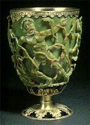

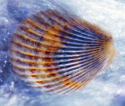
3 Lycurgus cup, British Museum Nanotechnology; even earlier days Nano-structures in nature Shell: nanobricks and nanoglue Nanomotors Nanostructure
 is nacre in red-abalone. (b) is synthetic ZnO crystals.")

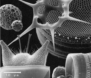
4 Complex nanostructed crystals have been prepared showing striking similarities with those observed in biominerals. (a) is nacre in red-abalone. (b) is synthetic ZnO crystals. (c) is a diatom. (d) to (h) are different types of synthetic silica crystals. The morphology depends on the growth conditions and can be controlled. Particle size dependent luminescence of CdSe


5 Applications of nanotechnology Medicine; diagnostics, therapy Genomics; sequencing? Ferrofluids Nano-electronics Actuators Nanorobots catalysis Nano-pants Self cleaning windows Nano-gear


6 Electronics-Spintronics Nanostructuring Top down or bottom up approach Physical methods: Electron beam lithography Physical thin film deposition Scanning tunneling microscopy Chemical methods: Self-organization/self assembly Nanoparticles Chemical thin film deposition


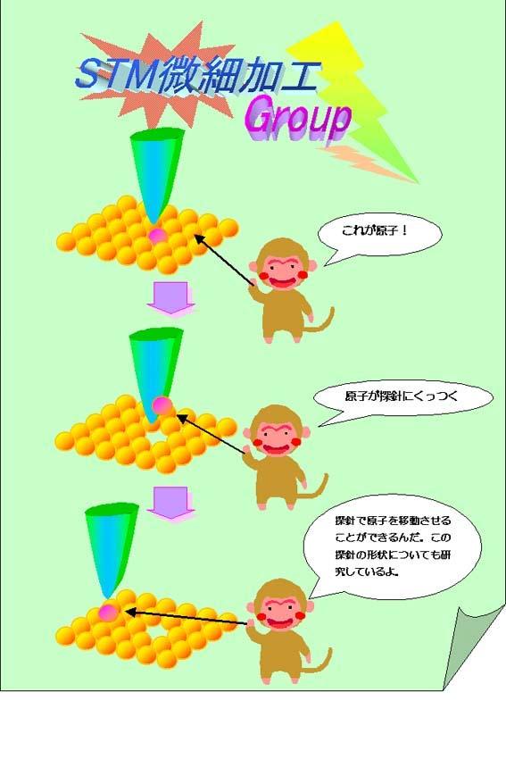
7 e-beam and deep UV lithography Scanning Tunneling Microscopy Single atom manipulation IBM
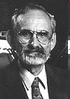
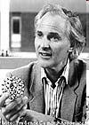
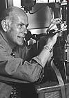
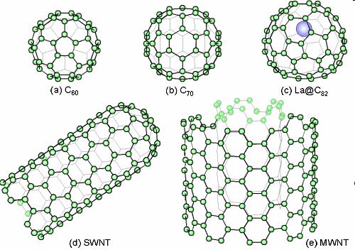
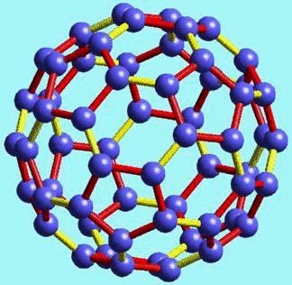
8 Fullerenes 1985 (1996) Robert F. Curl Jr. Richard E. Smalley Sir Harold W. Kroto
 Magnetoresistivity (low temperature) Mechanical properties; SWNT Young s modulus 10 times that of steel, 20 times stronger than steel SEM image of large arrays of")
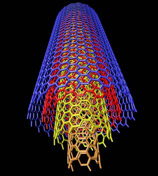
9 Properties of carbon nanotubes Single walled/multiwalled (SWNT/MWNT) Made by: Laser evaporation, carbon arc, Chemical Vapour Deposition Metallic/semiconducting depending on chirality High thermal conductivity (2 x diamond) Magnetoresistivity (low temperature) Mechanical properties; SWNT Young s modulus 10 times that of steel, 20 times stronger than steel SEM image of large arrays of well-aligned carbon nanotubes

 500nm 500nm")


10 Directional Metal Oxide Nanowires & Nanowalls Growth (Cont ) 500nm 500nm 2μm 925 C 1D Nanowire VLS growth 1μm Nanowall VLS growth Au surface diffusion & aggregation at a node Ng et al Science 300, 1249 (2003) Used in NASA presentations


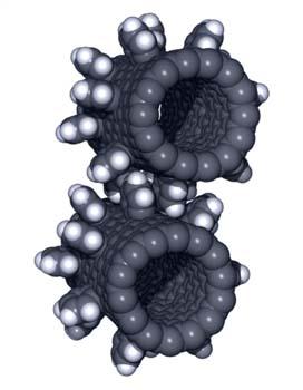
11 Gadolinium atoms in fullerenes in carbon nanotubes
12 Cubic crystal, diamond lattice type, n unit cells on one side n Size (nm) GaAs N atoms (total) N atoms (Surface) Percentage of surface atoms mm

13 Size dependent properties Melting point C Understanding Size 1 meter


14 Understanding Size 10 centimeters Understanding Size 1 centimeter


15 Understanding Size 100 micrometers Understanding Size 10 micrometers


16 Understanding Size 1 micrometer Understanding Size 100 nanometers


17 Understanding Size 10 nanometers Understanding Size 1 nanometer
Nanotechnology. An Introduction
 Nanotechnology An Introduction Nanotechnology A new interdisciplinary field of science The study of systems at the nanoscale The use of tools at the nanoscale Building and applying structures that are
Like space travel and the Internet before it, the possibilities of the nano world catches the imagination of school children and scientists alike.
 The Nano World Preface Nano is the cool thing and it s the buzzword Like space travel and the Internet before it, the possibilities of the nano world catches the imagination of school children and scientists
Nanotechnology Fabrication Methods.
 Nanotechnology Fabrication Methods. 10 / 05 / 2016 1 Summary: 1.Introduction to Nanotechnology:...3 2.Nanotechnology Fabrication Methods:...5 2.1.Top-down Methods:...7 2.2.Bottom-up Methods:...16 3.Conclusions:...19
Top down and bottom up fabrication
 Lecture 24 Top down and bottom up fabrication Lithography ( lithos stone / graphein to write) City of words lithograph h (Vito Acconci, 1999) 1930 s lithography press Photolithography d 2( NA) NA=numerical
Chapter 1 Introduction
 Chapter 1 Introduction A nanometer (nm) is one billionth (10-9 ) of a meter. Nanoscience can be defined as the science of objects and phenomena occurring at the scale of 1 to 100 nm. The range of 1 100
Nanotechnology. Yung Liou P601 Institute of Physics Academia Sinica
 Nanotechnology Yung Liou P601 yung@phys.sinica.edu.tw Institute of Physics Academia Sinica 1 1st week Definition of Nanotechnology The Interagency Subcommittee on Nanoscale Science, Engineering and Technology
Nanophysics: Main trends
 Nano-opto-electronics Nanophysics: Main trends Nanomechanics Main issues Light interaction with small structures Molecules Nanoparticles (semiconductor and metallic) Microparticles Photonic crystals Nanoplasmonics
1.0 Introduction. 1.1 Nanotechnology Historical Developments
 1.0 Introduction 1.1 Nanotechnology Historical Developments Around 370BC, Democritus a Greek philosopher developed the atomic theory of matter. Nano in GREEK means DWARF. The prefix nano means a billionth
Nano Materials and Devices
 Nano Materials and Devices Professor Michael Austin Platform Technologies Research Institute Nano Materials and Devices Program Aim: to develop an integrated capability in nanotechnology Design and modelling
In today s lecture, we will cover:
 In today s lecture, we will cover: Metal and Metal oxide Nanoparticles Semiconductor Nanocrystals Carbon Nanotubes 1 Week 2: Nanoparticles Goals for this section Develop an understanding of the physical
1. Introduction : 1.2 New properties:
 Nanodevices In Electronics Rakesh Kasaraneni(PID : 4672248) Department of Electrical Engineering EEL 5425 Introduction to Nanotechnology Florida International University Abstract : This paper describes
High-resolution Characterization of Organic Ultrathin Films Using Atomic Force Microscopy
 High-resolution Characterization of Organic Ultrathin Films Using Atomic Force Microscopy Jing-jiang Yu Nanotechnology Measurements Division Agilent Technologies, Inc. Atomic Force Microscopy High-Resolution
29: Nanotechnology. What is Nanotechnology? Properties Control and Understanding. Nanomaterials
 29: Nanotechnology What is Nanotechnology? Properties Control and Understanding Nanomaterials Making nanomaterials Seeing at the nanoscale Quantum Dots Carbon Nanotubes Biology at the Nanoscale Some Applications
Nanotechnology in Consumer Products
 Nanotechnology in Consumer Products June 17, 2015 October 31, 2014 The webinar will begin at 1pm Eastern Time Perform an audio check by going to Tools > Audio > Audio Setup Wizard Chat Box Chat Box Send
Nanotechnology. Gavin Lawes Department of Physics and Astronomy
 Nanotechnology Gavin Lawes Department of Physics and Astronomy Earth-Moon distance 4x10 8 m (courtesy NASA) Length scales (Part I) Person 2m Magnetic nanoparticle 5x10⁻⁹ m 10 10 m 10 5 m 1 m 10-5 m 10-10
In the name of Allah
 In the name of Allah Nano chemistry- 4 th stage Lecture No. 1 History of nanotechnology 16-10-2016 Assistance prof. Dr. Luma Majeed Ahmed lumamajeed2013@gmail.com, luma.ahmed@uokerbala.edu.iq Nano chemistry-4
Chapter 1. Introduction to Nanoparticle Technology. Nanoparticles the small particles with a big future.
 Chapter 1. Introduction to Nanoparticle Technology Nanoparticles the small particles with a big future. 1.1 Definitions Definition by size - Particles having sizes less than 0.1µm (100nm) 1 st generation
BIOMINERALIZATION: WHY ARE ABALONE SEASHELLS SO STRONG AND SHINY?
 BIOMINERALIZATION: WHY ARE ABALONE SEASHELLS SO STRONG AND SHINY? Belinda Hart Virginia A. Davis Department of Chemical Engineering Outline Doing one version of activity (another available as handout or
Contents. What is AFM? History Basic principles and devices Operating modes Application areas Advantages and disadvantages
 Contents What is AFM? History Basic principles and devices Operating modes Application areas Advantages and disadvantages Figure1: 2004 Seth Copen Goldstein What is AFM? A type of Scanning Probe Microscopy
C. Ruggiero Department of Communication Computer and System Sciences, University of Genoa, Italy
 NANOBIOTECHNOLOGY C. Ruggiero Department of Communication Computer and System Sciences, University of Genoa, Italy Keywords: Microtechnology, Nanotechnology, Nanoscale structures, Tunnelling Microscope,
Techniken der Oberflächenphysik (Technique of Surface Physics)
") Techniken der Oberflächenphysik (Technique of Surface Physics) Yong Lei & Fabian Grote Fachgebiet 3D-Nanostrukturierung, Institut für Physik Contact: yong.lei@tu-ilmenau.de; fabian.grote@tu-ilmenau.de
Techniken der Oberflächenphysik (Technique of Surface Physics) Yong Lei & Fabian Grote Fachgebiet 3D-Nanostrukturierung, Institut für Physik Contact: yong.lei@tu-ilmenau.de; fabian.grote@tu-ilmenau.de
Carbon nanomaterials. Gavin Lawes Wayne State University.
 Carbon nanomaterials Gavin Lawes Wayne State University glawes@wayne.edu Outline 1. Carbon structures 2. Carbon nanostructures 3. Potential applications for Carbon nanostructures Periodic table from bpc.edu
Introduction to Nanoscience and Nanotechnology
 Introduction to Nanoscience and Nanotechnology ENS 463 by Alexander M. Zaitsev alexander.zaitsev@csi.cuny.edu Tel: 718 982 2812 Office 4N101b 1 What is the size for a nano? 10-3 m, (milli) Macroobjects,
Chapter 10. Nanometrology. Oxford University Press All rights reserved.
 Chapter 10 Nanometrology Oxford University Press 2013. All rights reserved. 1 Introduction Nanometrology is the science of measurement at the nanoscale level. Figure illustrates where nanoscale stands
Seminars in Nanosystems - I
 Seminars in Nanosystems - I Winter Semester 2011/2012 Dr. Emanuela Margapoti Emanuela.Margapoti@wsi.tum.de Dr. Gregor Koblmüller Gregor.Koblmueller@wsi.tum.de Seminar Room at ZNN 1 floor Topics of the
Ali Ahmadpour. Fullerenes. Ali Ahmadpour. Department of Chemical Engineering Faculty of Engineering Ferdowsi University of Mashhad
 Ali Ahmadpour Fullerenes Ali Ahmadpour Department of Chemical Engineering Faculty of Engineering Ferdowsi University of Mashhad 2014 World of Carbon Materials 2 Fullerenes 1985 Robert F. Curl Jr. Richard
UFN Úvod do funkcionalizace nanomateriálů
 UFN Úvod do funkcionalizace nanomateriálů Zápočet, zkouška 2 Cvičení RNDr. Michal Řezanka, Ph.D. exkurze na konci semestru zápočet za 100% účast (v případě neúčasti referát na probírané téma) Přednášky
Introduction to Nanotechnology Chapter 5 Carbon Nanostructures Lecture 1
 Introduction to Nanotechnology Chapter 5 Carbon Nanostructures Lecture 1 ChiiDong Chen Institute of Physics, Academia Sinica chiidong@phys.sinica.edu.tw 02 27896766 Carbon contains 6 electrons: (1s) 2,
Nanotechnology? Source: National Science Foundation (NSF), USA
, USA") 2 2 Nanotechnology? Ability to work at the atomic, molecular and even sub-molecular levels in order to create and use material structures, devices and systems with new properties and functions Source:
2 2 Nanotechnology? Ability to work at the atomic, molecular and even sub-molecular levels in order to create and use material structures, devices and systems with new properties and functions Source:
Nanofabrication/Nano-Characterization Calixarene and CNT Control Technology
 Nanofabrication/Nano-Characterization Calixarene and CNT Control Technology ISHIDA Masahiko, FUJITA Junichi, NARIHIRO Mitsuru, ICHIHASHI Toshinari, NIHEY Fumiyuki, OCHIAI Yukinori Abstract The world of
materials, devices and systems through manipulation of matter at nanometer scale and exploitation of novel phenomena which arise because of the
 Nanotechnology is the creation of USEFUL/FUNCTIONAL materials, devices and systems through manipulation of matter at nanometer scale and exploitation of novel phenomena which arise because of the nanometer
Nanostructure. Materials Growth Characterization Fabrication. More see Waser, chapter 2
 Nanostructure Materials Growth Characterization Fabrication More see Waser, chapter 2 Materials growth - deposition deposition gas solid Physical Vapor Deposition Chemical Vapor Deposition Physical Vapor
ME 4875/MTE C/18. Introduction to Nanomaterials and Nanotechnology. Lecture 1 - Introduction
 ME 4875/MTE 575 - C/18 Introduction to Nanomaterials and Nanotechnology Lecture 1 - Introduction 1 Course Information Syllabus uploaded to Canvas Schedule: Lectures MT-RF 10:00-10:50 pm in Olin Hall 223
Graphene Fundamentals and Emergent Applications
 Graphene Fundamentals and Emergent Applications Jamie H. Warner Department of Materials University of Oxford Oxford, UK Franziska Schaffel Department of Materials University of Oxford Oxford, UK Alicja
ME 4875/MTE C/16. Introduction to Nanomaterials and Nanotechnology. Lecture 1 - Introduction
 ME 4875/MTE 575 - C/16 Introduction to Nanomaterials and Nanotechnology Lecture 1 - Introduction 1 Course Information Syllabus uploaded to mywpi Schedule: Lectures MT-RF 2:00-2:50 pm in Salisbury Labs
Crystalline Surfaces for Laser Metrology
 Crystalline Surfaces for Laser Metrology A.V. Latyshev, Institute of Semiconductor Physics SB RAS, Novosibirsk, Russia Abstract: The number of methodological recommendations has been pronounced to describe
SPECIFIC USES OR APPLICATIONS OF NANOSTRUCTURES; MEASUREMENT OR ANALYSIS OF NANOSTRUCTURES; MANUFACTURE OR TREATMENT OF NANOSTRUCTURES
 CPC - B82Y - 2017.08 B82Y SPECIFIC USES OR APPLICATIONS OF NANOSTRUCTURES; MEASUREMENT OR ANALYSIS OF NANOSTRUCTURES; MANUFACTURE OR TREATMENT OF NANOSTRUCTURES Definition statement This place covers:
Index. C 60 buckminsterfullerene 87 C 60 buckminsterfullerene formation process
 Index acetone 64 aluminum 64 65 arc-discharged carbon 25 argon ion laser 43 aromaticity 2D 99 3D 89 90, 98 planar 89 spherical 90 astronomy 113, 125, 127, 131 atoms chlorine 107 108 titanium 161 162 benzene
Nanomaterials and their Optical Applications
 Nanomaterials and their Optical Applications Winter Semester 2013 Lecture 02 rachel.grange@uni-jena.de http://www.iap.uni-jena.de/multiphoton Lecture 2: outline 2 Introduction to Nanophotonics Theoretical
Welcome to NANO* 2000
 Lecture Zero Welcome to NANO* 2000 First - the "big picture" of the course and the course outline -grading scheme - exam schedule - review paper - lab (Jay) last revision September 4 2013: MDB 0-1 NANO*
Appendix A. Assessments Points 4 Mode of Assessments. New Course Code and Title Course Coordinator. MS741M Nanomaterials
 New Course Code and Title Course Coordinator Details of Course MS741M Nanomaterials AP Jason Xu (Course Coordinator) AP Xue Can Rationale for introducing this course This course will cover the subject
Carbon Nanomaterials: Nanotubes and Nanobuds and Graphene towards new products 2030
 Carbon Nanomaterials: Nanotubes and Nanobuds and Graphene towards new products 2030 Prof. Dr. Esko I. Kauppinen Helsinki University of Technology (TKK) Espoo, Finland Forecast Seminar February 13, 2009
Nanostrukturphysik (Nanostructure Physics)
") Nanostrukturphysik (Nanostructure Physics) Yong Lei & Fabian Grote Fachgebiet 3D-Nanostrukturierung, Institut für Physik Contact: yong.lei@tu-ilmenau.de; fabian.grote@tu-ilmenau.de Office: Heliosbau 1102,
Nanostrukturphysik (Nanostructure Physics) Yong Lei & Fabian Grote Fachgebiet 3D-Nanostrukturierung, Institut für Physik Contact: yong.lei@tu-ilmenau.de; fabian.grote@tu-ilmenau.de Office: Heliosbau 1102,
Plasmonics. The long wavelength of light ( μm) creates a problem for extending optoelectronics into the nanometer regime.
 creates a problem for extending optoelectronics into the nanometer regime.") Plasmonics The long wavelength of light ( μm) creates a problem for extending optoelectronics into the nanometer regime. A possible way out is the conversion of light into plasmons. They have much shorter
Plasmonics The long wavelength of light ( μm) creates a problem for extending optoelectronics into the nanometer regime. A possible way out is the conversion of light into plasmons. They have much shorter
CSCI 2570 Introduction to Nanocomputing
 CSCI 2570 Introduction to Nanocomputing The Emergence of Nanotechnology John E Savage Purpose of the Course The end of Moore s Law is in sight. Researchers are now exploring replacements for standard methods
Nanotechnology where size matters
 Nanotechnology where size matters J Emyr Macdonald Overview Ways of seeing very small things What is nanotechnology and why is it important? Building nanostructures What we can do with nanotechnology?
1.1. Introduction to Nanoscience and Nanotechnology
 1.1. Introduction to Nanoscience and Nanotechnology 1.1.1. A Brief Historical Overview Before trying to understand and discuss about synthesis, characterization and application of nanomaterials, it is
Fullerenes Synthesis Using Fabricated Arc Discharge System with Relatively Large Chamber Size
 IOSR Journal of Applied Physics (IOSR-JAP) e-issn: 2278-4861.Volume 7, Issue 6 Ver. I (Nov. - Dec. 2015), PP 77-83 www.iosrjournals Fullerenes Synthesis Using Fabricated Arc Discharge System with Relatively
Image courtesy of Dr James Bendall, University of Cambridge, UK. Discover the secrets h of the Nanoworld
 Image courtesy of Dr James Bendall, University of Cambridge, UK. Discover the secrets h of the Nanoworld Nano has become a buzz word in popular culture to just mean small. To understand nanotechnology
I. NANOFABRICATION O AND CHARACTERIZATION Chap. 2 : Self-Assembly
 I. Nanofabrication and Characterization : TOC I. NANOFABRICATION O AND CHARACTERIZATION Chap. 1 : Nanolithography Chap. 2 : Self-Assembly Chap. 3 : Scanning Probe Microscopy Nanoscale fabrication requirements
Micro Chemical Vapor Deposition System: Design and Verification
 Micro Chemical Vapor Deposition System: Design and Verification Q. Zhou and L. Lin Berkeley Sensor and Actuator Center, Department of Mechanical Engineering, University of California, Berkeley 2009 IEEE
Fundamentals of nanoscience
 Fundamentals of nanoscience Spectroscopy of nano-objects Mika Pettersson 1. Non-spatially resolved spectroscopy Traditionally, in spectroscopy, one is interested in obtaining information on the energy
RAJASTHAN TECHNICAL UNIVERSITY, KOTA
 RAJASTHAN TECHNICAL UNIVERSITY, KOTA (Electronics & Communication) Submitted By: LAKSHIKA SOMANI E&C II yr, IV sem. Session: 2007-08 Department of Electronics & Communication Geetanjali Institute of Technical
Nano-mechatronics. Presented by: György BudaváriSzabó (X0LY4M)
") Nano-mechatronics Presented by: György BudaváriSzabó (X0LY4M) Nano-mechatronics Nano-mechatronics is currently used in broader spectra, ranging from basic applications in robotics, actuators, sensors,
Nano-mechatronics Presented by: György BudaváriSzabó (X0LY4M) Nano-mechatronics Nano-mechatronics is currently used in broader spectra, ranging from basic applications in robotics, actuators, sensors,
MSN551 LITHOGRAPHY II
 MSN551 Introduction to Micro and Nano Fabrication LITHOGRAPHY II E-Beam, Focused Ion Beam and Soft Lithography Why need electron beam lithography? Smaller features are required By electronics industry:
Techniken der Oberflächenphysik (Techniques of Surface Physics)
") Techniken der Oberflächenphysik (Techniques of Surface Physics) Prof. Yong Lei & Dr. Yang Xu, Dr. Huaping Zhao Fachgebiet Angewante Nanophysik, Institut für Physik Contact: yong.lei@tu-ilmenau.de yang.xu@tu-ilmenau.de
Techniken der Oberflächenphysik (Techniques of Surface Physics) Prof. Yong Lei & Dr. Yang Xu, Dr. Huaping Zhao Fachgebiet Angewante Nanophysik, Institut für Physik Contact: yong.lei@tu-ilmenau.de yang.xu@tu-ilmenau.de
Nanomaterials. Mechanical or chemical processing
 1 1 Introduction Everyone talks about nanomaterials. There are many publications, books and journals devoted to this topic. This is not surprising, as the economic importance is steadily increasing. Additionally,
D DAVID PUBLISHING. Study the Synthesis Parameter of Tin Oxide Nanostructure. 1. Introduction. 2. Experiment
 Journal of Materials Science and Engineering B 5 (9-10) (2015) 353-360 doi: 10.17265/2161-6221/2015.9-10.003 D DAVID PUBLISHING Study the Synthesis Parameter of Tin Oxide Nanostructure Gyanendra Prakash
The Dielectric Function of a Metal ( Jellium )
") The Dielectric Function of a Metal ( Jellium ) Total reflection Plasma frequency p (10 15 Hz range) Why are Metals Shiny? An electric field cannot exist inside a metal, because metal electrons follow the
The Dielectric Function of a Metal ( Jellium ) Total reflection Plasma frequency p (10 15 Hz range) Why are Metals Shiny? An electric field cannot exist inside a metal, because metal electrons follow the
Overview of the main nano-lithography techniques
 Overview of the main nano-lithography techniques Soraya Sangiao sangiao@unizar.es Outline Introduction: Nanotechnology. Nano-lithography techniques: Masked lithography techniques: Photolithography. X-ray
Lesson 4: Tools of the Nanosciences. Student Materials
 Lesson 4: Tools of the Nanosciences Student Materials Contents Black Box Lab Activity: Student Instructions and Worksheet Seeing and Building Small Things: Student Reading Seeing and Building Small Things:
Nanotechnology: Today and tomorrow
 Nanotechnology: Today and tomorrow Horst-Günter Rubahn NanoSYD Mads Clausen Instituttet Syddansk Universitet Alsion 2 6400 Sønderborg Agenda Alsion A bit about nano Nanoproducts Top down vs. bottom up
2.3 Modeling Interatomic Interactions Pairwise Potentials Many-Body Potentials Studying Biomolecules: The Force
 Contents 1 Introduction to Computational Meso-Bio-Nano (MBN) Science and MBN EXPLORER.... 1 1.1 Meso-Bio-Nano Science: A Novel Field of Interdisciplinary Research.... 1 1.1.1 Structure and Dynamics of
There's Plenty of Room at the Bottom
 There's Plenty of Room at the Bottom 12/29/1959 Feynman asked why not put the entire Encyclopedia Britannica (24 volumes) on a pin head (requires atomic scale recording). He proposed to use electron microscope
Nanotechnology Natural Engineering
 Natural Engineering The nanometer range is the size of molecules is simply molecular engineering Life itself can be viewed as being natural molecular engineers Oxygen generation The programming code of
Luminescent molecular clusters of noble metals
 Established in 1959 Luminescent molecular clusters of noble metals T. Pradeep Department of Chemistry Indian Institute of Technology Madras Chennai 600 036 pradeep@iitm.ac.in Quantum clusters: Au 25, Au
Chapter 12: Structures & Properties of Ceramics
 Chapter 12: Structures & Properties of Ceramics ISSUES TO ADDRESS... How do the crystal structures of ceramic materials differ from those for metals? How do point defects in ceramics differ from those
Carbon nanotubes and Graphene
 16 October, 2008 Solid State Physics Seminar Main points 1 History and discovery of Graphene and Carbon nanotubes 2 Tight-binding approximation Dynamics of electrons near the Dirac-points 3 Properties
Electrochemically Synthesized Multi-block
 Electrochemically Synthesized Multi-block Nanorods Sungho Park SungKyunKwan University, Department of Chemistry & SKKU Advanced Institute of Nanotechnology (SAINT) J. Am. Chem. Soc. 2003, 125, 2282-2290
Nanostructures Fabrication Methods
 Nanostructures Fabrication Methods bottom-up methods ( atom by atom ) In the bottom-up approach, atoms, molecules and even nanoparticles themselves can be used as the building blocks for the creation of
There s plenty of room at the bottom! - R.P. Feynman, Nanostructure: a piece of material with at least one dimension less than 100 nm in extent.
 Nanostructures and Nanotechnology There s plenty of room at the bottom! - R.P. Feynman, 1959 Materials behave differently when structured at the nm scale than they do in bulk. Technologies now exist that
Chapter 12. Nanometrology. Oxford University Press All rights reserved.
 Chapter 12 Nanometrology Introduction Nanometrology is the science of measurement at the nanoscale level. Figure illustrates where nanoscale stands in relation to a meter and sub divisions of meter. Nanometrology
High-temperature single-electron transistor based on a gold nanoparticle
 High-temperature single-electron transistor based on a gold nanoparticle SA Dagesyan 1 *, A S Stepanov 2, E S Soldatov 1, G Zharik 1 1 Lomonosov Moscow State University, faculty of physics, Moscow, Russia,
ME 4875/MTE C16. Introduction to Nanomaterials and Nanotechnology. Lecture 2 - Applications of Nanomaterials + Projects
 ME 4875/MTE 575 - C16 Introduction to Nanomaterials and Nanotechnology Lecture 2 - Applications of Nanomaterials + Projects 1 Project Teams of 4 students each Literature review of one application of nanotechnology
State of São Paulo. Brasil. Localization. Santo André
 Brasil State of São Paulo Localization Santo André The Group www.crespilho.com Frank N. Crespilho Pablo R. S. Abdias Group Leader Synthesis of nanostructured materials using polyelectrolytes Andressa R.
Nanotechnology Nanofabrication of Functional Materials. Marin Alexe Max Planck Institute of Microstructure Physics, Halle - Germany
 Nanotechnology Nanofabrication of Functional Materials Marin Alexe Max Planck Institute of Microstructure Physics, Halle - Germany Contents Part I History and background to nanotechnology Nanoworld Nanoelectronics
Technologies VII. Alternative Lithographic PROCEEDINGS OF SPIE. Douglas J. Resnick Christopher Bencher. Sponsored by. Cosponsored by.
 PROCEEDINGS OF SPIE Alternative Lithographic Technologies VII Douglas J. Resnick Christopher Bencher Editors 23-26 February 2015 San Jose, California, United States Sponsored by SPIE Cosponsored by DNS
Lecture 6. Alternative storage technologies. All optical recording. Racetrack memory. Topological kink solitons. Flash memory. Holographic memory
 Lecture 6 Alternative storage technologies All optical recording Racetrack memory Topological kink solitons Flash memory Holographic memory Millipede Ferroelectric memory All-optical recording It is possible
Fabrication at the nanoscale for nanophotonics
 Fabrication at the nanoscale for nanophotonics Ilya Sychugov, KTH Materials Physics, Kista silicon nanocrystal by electron beam induced deposition lithography Outline of basic nanofabrication methods Devices
SYLLABUS FINDING NANO Syllabus NanoSCI DISCOVERING NANOTECHNOLOGY AND CULTURE IN GERMANY
 1. Syllabus NanoSCI Course title: NanoSCI - Electronic Properties of Nanoengineered Materials Catalog description: Physics and technology of nanoengineered materials and devices. Semiconductor nanostructures.
Microscopy: Principles
 Low Voltage Electron Microscopy: Principles and Applications Edited by David C. Bell Harvard University, USA and Natasha Erdman JEOL USA Inc., USA Published in association with the Royal Microscopical
Carbon Nanotubes: The Hub Of Nanoelectronics
 Carbon Nanotubes: The Hub Of Nanoelectronics P.I. Okwu 1 and I.N. Onyeje 2 1 Deputy Director, Electronics Development Institute (ELDI) Awka, Nigeria 2 Department of Electrical/Electronic Engineering, Anambra
Localized surface plasmons (Particle plasmons)
") Localized surface plasmons (Particle plasmons) ( Plasmons in metal nanostructures, Dissertation, University of Munich by Carsten Sonnichsen, 2001) Lycurgus cup, 4th century (now at the British Museum,
Localized surface plasmons (Particle plasmons) ( Plasmons in metal nanostructures, Dissertation, University of Munich by Carsten Sonnichsen, 2001) Lycurgus cup, 4th century (now at the British Museum,
From nanophysics research labs to cell phones. Dr. András Halbritter Department of Physics associate professor
 From nanophysics research labs to cell phones Dr. András Halbritter Department of Physics associate professor Curriculum Vitae Birth: 1976. High-school graduation: 1994. Master degree: 1999. PhD: 2003.
SELF-ASSEMBLY AND NANOTECHNOLOGY A Force Balance Approach
 SELF-ASSEMBLY AND NANOTECHNOLOGY A Force Balance Approach Yoon S. Lee Scientific Information Analyst Chemical Abstracts Service A Division of the American Chemical Society Columbus, Ohio WILEY A JOHN WILEY
OCR A GCSE Chemistry. Topic 2: Elements, compounds and mixtures. Properties of materials. Notes.
 OCR A GCSE Chemistry Topic 2: Elements, compounds and mixtures Properties of materials Notes C2.3a recall that carbon can form four covalent bonds C2.3b explain that the vast array of natural and synthetic
7. Carbon Nanotubes. 1. Overview: Global status market price 2. Types. 3. Properties. 4. Synthesis. MWNT / SWNT zig-zag / armchair / chiral
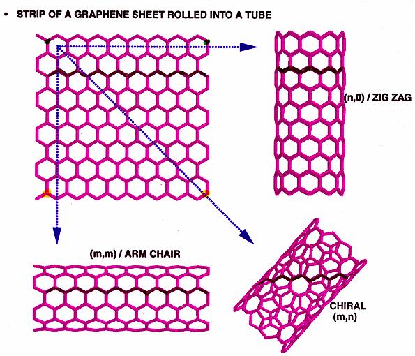
 7. Carbon Nanotubes 1. Overview: Global status market price 2. Types MWNT / SWNT zig-zag / armchair / chiral 3. Properties electrical others 4. Synthesis arc discharge / laser ablation / CVD 5. Applications
NANOMEDICINE. WILEY A John Wiley and Sons, Ltd., Publication DESIGN AND APPLICATIONS OF MAGNETIC NANOMATERIALS, NANOSENSORS AND NANOSYSTEMS
 NANOMEDICINE DESIGN AND APPLICATIONS OF MAGNETIC NANOMATERIALS, NANOSENSORS AND NANOSYSTEMS Vijay K. Varadan Linfeng Chen Jining Xie WILEY A John Wiley and Sons, Ltd., Publication Preface About the Authors
NANOSCIENCE AND NANOTECHNOLOGY
 NANOSCIENCE AND NANOTECHNOLOGY Yuehe Lin WHAT IS NANOTECHNOLOGY Nanotechnology is the understanding and control of matter at dimensions of roughly 1 to 100 nanometers, where unique phenomena enable novel
Scanning Tunneling Microscopy
 Scanning Tunneling Microscopy References: 1. G. Binnig, H. Rohrer, C. Gerber, and Weibel, Phys. Rev. Lett. 49, 57 (1982); and ibid 50, 120 (1983). 2. J. Chen, Introduction to Scanning Tunneling Microscopy,
Chapter 3 History of Nanotechnologies
 NANOYOU Teachers Training Kit in Nanoscience and Nanotechnologies Chapter 3 History of Nanotechnologies Module 1- Fundamental concepts in nanoscience and nanotechnologies Written by Luisa Filipponi and
Nanostrukturphysik (Nanostructure Physics)
") Nanostrukturphysik (Nanostructure Physics) Prof. Yong Lei & Dr. Yang Xu Fachgebiet 3D-Nanostrukturierung, Institut für Physik Contact: yong.lei@tu-ilmenau.de; yang.xu@tu-ilmenau.de Office: Unterpoerlitzer
Nanostrukturphysik (Nanostructure Physics) Prof. Yong Lei & Dr. Yang Xu Fachgebiet 3D-Nanostrukturierung, Institut für Physik Contact: yong.lei@tu-ilmenau.de; yang.xu@tu-ilmenau.de Office: Unterpoerlitzer
Size and Zeta Potential of Colloidal Gold Particles
 Size and Zeta Potential of Colloidal Gold Particles Mark Bumiller mark.bumiller@horiba.com Colloid Definition Two phases: Dispersed phase (particles) Continuous phase (dispersion medium, solvent) May be
7. Localized surface plasmons (Particle plasmons)
") 7. Localized surface plasmons (Particle plasmons) ( Plasmons in metal nanostructures, Dissertation, University of Munich by Carsten Sonnichsen, 2001) Lycurgus cup, 4th century (now at the British Museum,
7. Localized surface plasmons (Particle plasmons) ( Plasmons in metal nanostructures, Dissertation, University of Munich by Carsten Sonnichsen, 2001) Lycurgus cup, 4th century (now at the British Museum,
Nanostructures. Nanomaterials Synthesis, Properties, and Applications
 Nanostructures and Nanomaterials Synthesis, Properties, and Applications 2nd Edition World Scientific Series in Nanoscience and Nanotechnology Series Editor: Mark Reed (Yale University) Vol. 1 Vol. 2 Molecular
Self-assembled nanostructures for antireflection optical coatings
 Self-assembled nanostructures for antireflection optical coatings Yang Zhao 1, Guangzhao Mao 2, and Jinsong Wang 1 1. Deaprtment of Electrical and Computer Engineering 2. Departmentof Chemical Engineering
Laser and Plasma-based Nanotechnologies
 Simpozionul: De la excelenta la competitivitate: tehnologiile generice esentiale Aula Academiei Romane, Bucuresti 15 mai 2014. Laser and Plasma-based Nanotechnologies Marian ZAMFIRESCU National Institute
Nanoscale Issues in Materials & Manufacturing
 Nanoscale Issues in Materials & Manufacturing ENGR 213 Principles of Materials Engineering Module 2: Introduction to Nanoscale Issues Top-down and Bottom-up Approaches for Fabrication Winfried Teizer,
NANOTECHNOLOGY. Students will gain an understanding of nanoscale dimensions and nanotechnology.
 NANOTECHNOLOGY By Anna M. Waldron and Carl A. Batt, Nanobiotechnology Center, Cornell University Subjects: Nanotechnology, Chemistry, Physics Time: Two class periods (approximately 90 minutes) Objective:
Lecture 6: Individual nanoparticles, nanocrystals and quantum dots
 Lecture 6: Individual nanoparticles, nanocrystals and quantum dots Definition of nanoparticle: Size definition arbitrary More interesting: definition based on change in physical properties. Size smaller