Nanostrutture a base di Si e Ge per nuovi dispositivi nano-elettronici
|
|
|
- Marybeth Manning
- 5 years ago
- Views:
Transcription

 www.mdm.")
1 Nanostrutture a base di Si e Ge per nuovi dispositivi nano-elettronici Alberto Debernardi Laboratorio MDM, IMM-CNR Agrate Brianza (Italy)
2 Plan of the talk Scaling down electronic devices (Moore s law) P or Se doped Si-nanowires for quantum computing Delocalization of P(Se) wave-function Si NW [001], [011], [111] oriented Ab initio spectroscopy (Hyperfine parameters, MOKE) Conclusion and Discussion 2


3 Scaling down of CMOS logic devices Moore s law The number of components in a single chip doubles every 18 months 3


4 Scaling down of CMOS logic devices INTEL Presentation SPIE 03/2003 La dimensione dei chip si riduce constantemente International Technology Roadmap for Semiconductors (ITRS) fino a raggiungere le dimensioni atomiche?! 4
5 Scaling down of electronic devices Ultra-scaled CMOS devices Three strategies More than Moore, new concept for ultrascaled devices Moore s law Nanodevices whose size is a few nanometers Quantum effect are relevant first principles simulations techniques Nano structures as building block of novel device 5
 Stanene (Sn)")

6 Grafene (C) Silicene (Si) Germanene (Ge) Stanene (Sn) Dispositivi ultra-veloci Nuovi Sensori Nuova elettronica 6


 What are the")
7 Si-Nanostructures Applications Ultra-scaled electronic devices Gate controlled quantum dot Photovoltaics Quantum computation Nanosensors (DNA,...) What are the limits of Conventional computing? 7
![Density Functional Theory For a give external potential Target: to compute the total energy v r E[n] Total energy is a unique](/docs-images/92/110149190/images/8-1.jpg "functional of the density Plane-waves pseudopotential techniques E[n] = ε v 1 2 n r n r r' r' d rd r' + E xc [n] v r n r d r")
8 Density Functional Theory For a give external potential Target: to compute the total energy v r E[n] Total energy is a unique functional of the density Plane-waves pseudopotential techniques E[n] = ε v 1 2 n r n r r' r' d rd r' + E xc [n] v r n r d r 8
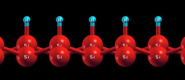
9 Single atom electronics: Se impurity Se doped H passivated Si nanowires (nanoelectronics, quantum computer) front view side view 9


10 Nanowire passivation 10

11 H passivated Si nanowires Relaxed Passivated and Relaxed again Distortion of NW for smal size is significant. Passivated and relaxed 11
 12")
12 Se doped Si nanowires One dimensional bandstructure Impurity level in the bandgap Correction to periodically repeated charged imeges (Rurali et al, Makov-Payne) 12
13 Band-gap of Si nano-wire Band-gap as a function of NW diameter Trangles: NW with surface reconstruction Squares: NW without surface reconstruction As an effect of confinemente the Bandgap increases as the diameter is reduced 13
![Delocalization of donor wave-funnction [001] Three orientations](/docs-images/92/110149190/images/14-1.jpg "considered [011] Diameter: 1.2-1.")
14 Delocalization of donor wave-funnction [001] Three orientations considered [011] Diameter: nm passivatedrelaxed [111] 14
![Delocalization of donor wave-funnction a z Ψ z 2 Ψ [001] a z = Ψ x, y, z 2 z 2 dxdydx [011] LUMO of](/docs-images/92/110149190/images/15-1.jpg "ionized system (Niquet et al, 2010).")
15 Delocalization of donor wave-funnction a z Ψ z 2 Ψ [001] a z = Ψ x, y, z 2 z 2 dxdydx [011] LUMO of ionized system (Niquet et al, 2010). But HOMO of neutral system gives the same qualitative results [111] 15
16 Delocalization of donor wave-function The a z of Se wave-function is computed The a z of Se wave-function for [011] should be extrapolated f z, L = e z2 a + c 16
![Delocalization of donor wave-function The large delocalization of P wave-function along [011] direction Si: P bulk a](/docs-images/92/110149190/images/17-1.jpg "z ~ 25 A [111] [011] Se P a z [001] < a z [111] < a z [011] [001].we suggest it is a general tends 0 5 10 a z (Å) 17")
17 Delocalization of donor wave-function The large delocalization of P wave-function along [011] direction Si: P bulk a z ~ 25 A [111] [011] Se P a z [001] < a z [111] < a z [011] [001].we suggest it is a general tends a z (Å) 17
18 Strain along the NW axis The a z of Se: non linear dependence of the strain The a z of P: strong dependence Modification of shallow wave-function by strain 18

19 Strain along the NW axis Quantum computing P Se +6% The interaction between neighbour P can be tuned by piezoelectrical actuators Unstrained -6% 19
20 Conclusions The [011] is the best direction for nano-electronic and quantum computing applications Stress allow to tune delocalization 20
21 Ab initio spectroscopy Interazione luce-materia predizioni senza parametri aggiustabili Permette l analisi dei dati sperimantali Individua i meccanismi microscopici responsabili di una data proprietà Predice quali sono le condizioni ottimali per ottenere un dato fenomeno E più economica di un «vero» esperimento 21

22 Ab initio spectroscopy: MOKE MOKE spectra by plane-wave pseudopotential techniques Simulation of relatively large systems our work all electron (Delin et al.) **** experiment Bulk Fe 22
 Esperimento Teoria")
23 Ab initio spectroscopy: XAS Interazione luce-materia, predizioni senza parametri aggiustabili ZrO2:Fe Diluted Magnetic Oxide for spintronic applications (film di 29 nm) Esperimento Teoria 23
 ( ) ( 3 4 3 r r n r d S g g A s z N N e e iso 2 2, 3, 3 ) ( 2 r r r r r n r d S g g A j i j i s z N N e e j i dip b b b b b A dip 2 '")
24 24 Hyperfine coupling constant: Charged defects Hyperfine interaction requires a spin density 0 Ionization of the impurity A iso A dip A 1 ) ( ) ( r r n r d S g g A s z N N e e iso 2 2, 3, 3 ) ( 2 r r r r r n r d S g g A j i j i s z N N e e j i dip b b b b b A dip 2 ' '

")
25 Si(Ge) dots:s + contact term Si-NC:S + (1) Si-NC:S + (2) 25
26 Single atom electronics: Se impurity Se doped H passivated Si nanowires (nanoelectronics, quantum computer) front view side view 26
27 Hyperfine coupling constants: axial Se Confinement enhances the hyperfine coupling constant Central impurity [001] NW1 NW2 NW3 NW4 1 NW5 0 NW6-1 d (nm) Aiso (GHz) b (MHz) Note: b is MHz for NW1, and negligible (< 0.22) for all the others 27

28 Se doped Si-NW HFC couples nuclear and electron spin Quantum bits (qu-bits) are stored in the nuclear spin of Se atom Distortion of NW for smal size is significant. Increase of HFC of about 30% at optimum diameter 28
 on the basis of EPR SPECTRA")
29 Isotropic Hyperfine Coupling STRONG DEPENDENCE OF HYPERFINE CONSTANT ON IMPURITY SITE It is possible to DETERMINE the POSITION of the impurity (Se) on the basis of EPR SPECTRA 29

30 Magnetic Semiconductor Silicane: 30
31 Proprietà Ottiche Magneto Optical Kerr Effect Magnetism Funzione dielettrica 31
32 Conclusions The position of the impurity can be determined by comparing EPR spectra with ab initio data MOKE signal in 2D for future nano-electronic devices La Simulazione è MOLTO più economica dell esperimento Possiamo «inventare» nuovi materiali e modificarne le proprietà per una nuova elettronica. 32
33 A special thanks to G. Petretto, A. Masse (IMM-CNR, University of Milano Bicocca) L. Marchetti, P. Rosa (IMM-CNR, University of Milano Statale) D.Douma, D.Sangalli (IMM-CNR) M. Fanciulli (UNIMIB, MDM) and to all experimentalists at the MDM laboratory. LISA for computational resources and you for your attention!!! 33

34 S doped Si Nano Dots 34
35 Se doped Si NW: Formation Energy Subsurface position is energergetic ally favoured (at least for small diameter) Effect of distortion for small diameters 35
36 Stability of ionized Se Formation energy of the defect on the axis of the nanowire as a function of the chemical potential. The three graphs represent the three different nanowires with diameter 1.2 nm, 1.5 nm, 2.0 nm respectively. The zero value is the calculated value of the formation energy of Se defect in bulk Si. 36
Properties and applications of ferromagnetic nanostructures
 Properties and applications of ferromagnetic nanostructures Diego Bisero, Lucia Del Bianco, Federico Spizzo Magnetism Experimental group Outline 1.Nanostructures: some examples 2.Why ferromagnetic nanostructures?
Electronic and Optoelectronic Properties of Semiconductor Structures
 Electronic and Optoelectronic Properties of Semiconductor Structures Jasprit Singh University of Michigan, Ann Arbor CAMBRIDGE UNIVERSITY PRESS CONTENTS PREFACE INTRODUCTION xiii xiv 1.1 SURVEY OF ADVANCES
Challenges for Materials to Support Emerging Research Devices
 Challenges for Materials to Support Emerging Research Devices C. Michael Garner*, James Hutchby +, George Bourianoff*, and Victor Zhirnov + *Intel Corporation Santa Clara, CA + Semiconductor Research Corporation
Outline. Introduction: graphene. Adsorption on graphene: - Chemisorption - Physisorption. Summary
 Outline Introduction: graphene Adsorption on graphene: - Chemisorption - Physisorption Summary 1 Electronic band structure: Electronic properties K Γ M v F = 10 6 ms -1 = c/300 massless Dirac particles!
 Image courtesy of Keith Schwab http://www.lbl.gov/science-articles/archive/afrd Articles/Archive/AFRD-quantum-logic.html http://www.wmi.badw.de/sfb631/tps/dqd2.gif http://qist.lanl.gov/qcomp_map.shtml
Directions for simulation of beyond-cmos devices. Dmitri Nikonov, George Bourianoff, Mark Stettler
 Directions for simulation of beyond-cmos devices Dmitri Nikonov, George Bourianoff, Mark Stettler Outline Challenges and responses in nanoelectronic simulation Limits for electronic devices and motivation
SIMULATIONS ON DILUTE MAGNETIC SEMICONDUCTOR PROPERTIES
 Romanian Reports in Physics, Vol. 62, No. 1, P. 115 120, 2010 SIMULATIONS ON DILUTE MAGNETIC SEMICONDUCTOR PROPERTIES M. NEGOITA, E. A. PATROI, C. V. ONICA National Institute for Research and Development
1. Nanotechnology & nanomaterials -- Functional nanomaterials enabled by nanotechnologies.
 Novel Nano-Engineered Semiconductors for Possible Photon Sources and Detectors NAI-CHANG YEH Department of Physics, California Institute of Technology 1. Nanotechnology & nanomaterials -- Functional nanomaterials
INVESTIGATIONS OF Mn, Fe, Ni AND Pb DOPED
 INVESTIGATIONS OF Mn, Fe, Ni AND Pb DOPED ZINC SULPHIDE NANOPARTICLES A thesis submitted to the University of Pune FOR THE DEGREE OF DOCTOR of PHILOSOPHY IN PHYSICS by PRAMOD H. BORSE DEPARTMENT OF PHYSICS
Shallow Donors in Silicon as Electron and Nuclear Spin Qubits Johan van Tol National High Magnetic Field Lab Florida State University
 Shallow Donors in Silicon as Electron and Nuclear Spin Qubits Johan van Tol National High Magnetic Field Lab Florida State University Overview Electronics The end of Moore s law? Quantum computing Spin
Electroluminescence from Silicon and Germanium Nanostructures
 Electroluminescence from silicon Silicon Getnet M. and Ghoshal S.K 35 ORIGINAL ARTICLE Electroluminescence from Silicon and Germanium Nanostructures Getnet Melese* and Ghoshal S. K.** Abstract Silicon
Semiconducting nano-composites for solar energy conversion: insights from ab initio calculations. S. Wippermann, G. Galli
 Semiconducting nano-composites for solar energy conversion: insights from ab initio calculations S. Wippermann, G. Galli ICAMP-12, 08/10/2012 Search for materials to harvest light: Desperately seeking
Minimal Update of Solid State Physics
 Minimal Update of Solid State Physics It is expected that participants are acquainted with basics of solid state physics. Therefore here we will refresh only those aspects, which are absolutely necessary
Fundamentals of Nanoelectronics: Basic Concepts
 Fundamentals of Nanoelectronics: Basic Concepts Sławomir Prucnal FWIM Page 1 Introduction Outline Electronics in nanoscale Transport Ohms law Optoelectronic properties of semiconductors Optics in nanoscale
Federico Chinni Curriculum vitae
 Federico Chinni Curriculum vitae Via Torleone 24, Bologna (Italy) CAP 40125 +39 347 8374882 +39 0534 29150 federico.chinni89@gmail.com Personal Information Date of Birth Porretta Terme, Nationality Italian
Second harmonic generation in silicon waveguides strained by silicon nitride
 Second harmonic generation in silicon waveguides strained by silicon nitride M. Cazzanelli, 1 F. Bianco, 1 E. Borga, 1 G. Pucker, 2 M. Ghulinyan, 2 E. Degoli, 3 E. Luppi, 4,7 V. Véniard, 4 S. Ossicini,
RAJASTHAN TECHNICAL UNIVERSITY, KOTA
 RAJASTHAN TECHNICAL UNIVERSITY, KOTA (Electronics & Communication) Submitted By: LAKSHIKA SOMANI E&C II yr, IV sem. Session: 2007-08 Department of Electronics & Communication Geetanjali Institute of Technical
Luminescence Process
 Luminescence Process The absorption and the emission are related to each other and they are described by two terms which are complex conjugate of each other in the interaction Hamiltonian (H er ). In an
Recap (so far) Low-Dimensional & Boundary Effects
 Low-Dimensional & Boundary Effects") Recap (so far) Ohm s & Fourier s Laws Mobility & Thermal Conductivity Heat Capacity Wiedemann-Franz Relationship Size Effects and Breakdown of Classical Laws 1 Low-Dimensional & Boundary Effects Energy
Recap (so far) Ohm s & Fourier s Laws Mobility & Thermal Conductivity Heat Capacity Wiedemann-Franz Relationship Size Effects and Breakdown of Classical Laws 1 Low-Dimensional & Boundary Effects Energy
NBTI and Spin Dependent Charge Pumping in 4H-SiC MOSFETs
 NBTI and Spin Dependent Charge Pumping in 4H-SiC MOSFETs Mark A. Anders, Patrick M. Lenahan, Pennsylvania State University Aivars Lelis, US Army Research Laboratory Energy Deviations from the resonance
OMEN an atomistic and full-band quantum transport simulator for post-cmos nanodevices
 Purdue University Purdue e-pubs Other Nanotechnology Publications Birck Nanotechnology Center 8-18-28 OMEN an atomistic and full-band quantum transport simulator for post-cmos nanodevices Mathieu Luisier
CITY UNIVERSITY OF HONG KONG. Theoretical Study of Electronic and Electrical Properties of Silicon Nanowires
 CITY UNIVERSITY OF HONG KONG Ë Theoretical Study of Electronic and Electrical Properties of Silicon Nanowires u Ä öä ªqk u{ Submitted to Department of Physics and Materials Science gkö y in Partial Fulfillment
PHYSICS OF SEMICONDUCTORS AND THEIR HETEROSTRUCTURES
 PHYSICS OF SEMICONDUCTORS AND THEIR HETEROSTRUCTURES Jasprit Singh University of Michigan McGraw-Hill, Inc. New York St. Louis San Francisco Auckland Bogota Caracas Lisbon London Madrid Mexico Milan Montreal
Chapter 3 Properties of Nanostructures
 Chapter 3 Properties of Nanostructures In Chapter 2, the reduction of the extent of a solid in one or more dimensions was shown to lead to a dramatic alteration of the overall behavior of the solids. Generally,
Nuclear spin spectroscopy for semiconductor hetero and nano structures
 (Interaction and Nanostructural Effects in Low-Dimensional Systems) November 16th, Kyoto, Japan Nuclear spin spectroscopy for semiconductor hetero and nano structures Yoshiro Hirayama Tohoku University
Spintronics. Seminar report SUBMITTED TO: SUBMITTED BY:
 A Seminar report On Spintronics Submitted in partial fulfillment of the requirement for the award of degree of Electronics SUBMITTED TO: SUBMITTED BY: www.studymafia.org www.studymafia.org Preface I have
Nanoimprint Lithography
 Nanoimprint Lithography Wei Wu Quantum Science Research Advanced Studies HP Labs, Hewlett-Packard Email: wei.wu@hp.com Outline Background Nanoimprint lithography Thermal based UV-based Applications based
Surfaces, Interfaces, and Layered Devices
 Surfaces, Interfaces, and Layered Devices Building blocks for nanodevices! W. Pauli: God made solids, but surfaces were the work of Devil. Surfaces and Interfaces 1 Role of surface effects in mesoscopic
Lecture 7: Extrinsic semiconductors - Fermi level
 Lecture 7: Extrinsic semiconductors - Fermi level Contents 1 Dopant materials 1 2 E F in extrinsic semiconductors 5 3 Temperature dependence of carrier concentration 6 3.1 Low temperature regime (T < T
Plasmon enhanced UV electroluminescence in SiO 2 with percolating conduction sustained by free-exciton emitting SnO 2 nanoparticles
 Dipartimento di Scienza dei Materiali Università di Milano-Bicocca TITLE Plasmon enhanced UV electroluminescence in O 2 with percolating conduction sustained by free-exciton emitting SnO 2 nanoparticles
How a single defect can affect silicon nano-devices. Ted Thorbeck
 How a single defect can affect silicon nano-devices Ted Thorbeck tedt@nist.gov The Big Idea As MOS-FETs continue to shrink, single atomic scale defects are beginning to affect device performance Gate Source
EXTRINSIC SEMICONDUCTOR
 EXTRINSIC SEMICONDUCTOR In an extrinsic semiconducting material, the charge carriers originate from impurity atoms added to the original material is called impurity [or] extrinsic semiconductor. This Semiconductor
QUANTUM WELLS, WIRES AND DOTS
 QUANTUM WELLS, WIRES AND DOTS Theoretical and Computational Physics of Semiconductor Nanostructures Second Edition Paul Harrison The University of Leeds, UK /Cf}\WILEY~ ^INTERSCIENCE JOHN WILEY & SONS,
quantum mechanics is a hugely successful theory... QSIT08.V01 Page 1
 1.0 Introduction to Quantum Systems for Information Technology 1.1 Motivation What is quantum mechanics good for? traditional historical perspective: beginning of 20th century: classical physics fails
Basic cell design. Si cell
 Basic cell design Si cell 1 Concepts needed to describe photovoltaic device 1. energy bands in semiconductors: from bonds to bands 2. free carriers: holes and electrons, doping 3. electron and hole current:
1.0 Introduction to Quantum Systems for Information Technology 1.1 Motivation
 QSIT09.V01 Page 1 1.0 Introduction to Quantum Systems for Information Technology 1.1 Motivation What is quantum mechanics good for? traditional historical perspective: beginning of 20th century: classical
NANOELECTRONICS AND PLASMA PROCESSING THE NEXT 15 YEARS AND BEYOND. Department of Electrical Engineering and Computer Sciences
 NANOELECTRONICS AND PLASMA PROCESSING THE NEXT 15 YEARS AND BEYOND M.A. Lieberman Department of Electrical Engineering and Computer Sciences University of California Berkeley, CA 94720 Download this talk:
Crosslight Software Overview, New Features & Updates. Dr. Peter Mensz
 1 Crosslight Software Overview, New Features & Updates Dr. Peter Mensz 2 Device Simulators Lastip/Pics3d Laser diode FEM models in 2D/3D Apsys 2D and 3D Any other compound semiconductors device FEM models,
Lecture contents. Stress and strain Deformation potential. NNSE 618 Lecture #23
 1 Lecture contents Stress and strain Deformation potential Few concepts from linear elasticity theory : Stress and Strain 6 independent components 2 Stress = force/area ( 3x3 symmetric tensor! ) ij ji
EE410 vs. Advanced CMOS Structures
 EE410 vs. Advanced CMOS Structures Prof. Krishna S Department of Electrical Engineering S 1 EE410 CMOS Structure P + poly-si N + poly-si Al/Si alloy LPCVD PSG P + P + N + N + PMOS N-substrate NMOS P-well
Review of Optical Properties of Materials
 Review of Optical Properties of Materials Review of optics Absorption in semiconductors: qualitative discussion Derivation of Optical Absorption Coefficient in Direct Semiconductors Photons When dealing
Variation of Electronic State of CUBOID Quantum Dot with Size
 Nano Vision, Vol.1 (1), 25-33 (211) Variation of Electronic State of CUBOID Quantum Dot with Size RAMA SHANKER YADAV and B. S. BHADORIA* Department of Physics, Bundelkhand University, Jhansi-284128 U.P.
Supplementary information for the paper
 Supplementary information for the paper Structural correlations in the generation of polaron pairs in lowbandgap polymers for photovoltaics Supplementary figures Chemically induced OD 0,1 0,0-0,1 0,1 0,0-0,1
Physical Properties of Mono-layer of
 Chapter 3 Physical Properties of Mono-layer of Silicene The fascinating physical properties[ 6] associated with graphene have motivated many researchers to search for new graphene-like two-dimensional
Mn in GaAs: from a single impurity to ferromagnetic layers
 Mn in GaAs: from a single impurity to ferromagnetic layers Paul Koenraad Department of Applied Physics Eindhoven University of Technology Materials D e v i c e s S y s t e m s COBRA Inter-University Research
The Role of Hydrogen on Dielectric Properties of Silicon Nanoclusters
 The Role of Hydrogen on Dielectric Properties of Silicon Nanoclusters Sib Krishna Ghoshal 1, M. R. Sahar 2, R. Arifin 3, K. Hamzah 4 1,2,3,4 Advanced Optical Material Research Group, Department of Physics,
Chapter 1 Electronic and Photonic Materials - DMS. Diluted Magnetic Semiconductor (DMS)
") Diluted Magnetic Semiconductor (DMS) 1 Properties of electron Useful! Charge Electron Spin? Mass 2 Schematic of a Spinning & Revolving Particle Spinning Revolution 3 Introduction Electronics Industry Uses
Diluted Magnetic Semiconductor (DMS) 1 Properties of electron Useful! Charge Electron Spin? Mass 2 Schematic of a Spinning & Revolving Particle Spinning Revolution 3 Introduction Electronics Industry Uses
Advanced Topics In Solid State Devices EE290B. Will a New Milli-Volt Switch Replace the Transistor for Digital Applications?
 Advanced Topics In Solid State Devices EE290B Will a New Milli-Volt Switch Replace the Transistor for Digital Applications? August 28, 2007 Prof. Eli Yablonovitch Electrical Engineering & Computer Sciences
Surfaces, Interfaces, and Layered Devices
 Surfaces, Interfaces, and Layered Devices Building blocks for nanodevices! W. Pauli: God made solids, but surfaces were the work of Devil. Surfaces and Interfaces 1 Interface between a crystal and vacuum
Electron Emission from Diamondoids: a DMC Study. Neil D. Drummond Andrew J. Williamson Richard J. Needs and Giulia Galli
 Electron Emission from Diamondoids: a DMC Study Neil D. Drummond Andrew J. Williamson Richard J. Needs and Giulia Galli October 18, 2005 1 Semiconductor Nanoparticles for Optoelectronic Devices (I) The
Single ion implantation for nanoelectronics and the application to biological systems. Iwao Ohdomari Waseda University Tokyo, Japan
 Single ion implantation for nanoelectronics and the application to biological systems Iwao Ohdomari Waseda University Tokyo, Japan Contents 1.History of single ion implantation (SII) 2.Novel applications
3/10/2013. Lecture #1. How small is Nano? (A movie) What is Nanotechnology? What is Nanoelectronics? What are Emerging Devices?
 What is Nanotechnology? What is Nanoelectronics? What are Emerging Devices?") EECS 498/598: Nanocircuits and Nanoarchitectures Lecture 1: Introduction to Nanotelectronic Devices (Sept. 5) Lectures 2: ITRS Nanoelectronics Road Map (Sept 7) Lecture 3: Nanodevices; Guest Lecture by
EECS 498/598: Nanocircuits and Nanoarchitectures Lecture 1: Introduction to Nanotelectronic Devices (Sept. 5) Lectures 2: ITRS Nanoelectronics Road Map (Sept 7) Lecture 3: Nanodevices; Guest Lecture by
Effect of the High-k Dielectric/Semiconductor Interface on Electronic Properties in Ultra-thin Channels
 Effect of the High-k Dielectric/Semiconductor Interface on Electronic Properties in Ultra-thin Channels Evan Wilson, Daniel Valencia, Mark J. W. Rodwell, Gerhard Klimeck and Michael Povolotskyi Electrical
Special Topics in Semiconductor Nanotechnology ECE 598XL
 Special Topics in Semiconductor Nanotechnology ECE 598XL Fall 2009 ECE 598XL Syllabus Overview: size matters Formation Process Characterization SOA device applications and potentials Homework or quizzes
DISTRIBUTION STATEMENT A
 ASIAA/CCMS/IAMS/LeCosPA/NTU Phys Joint Colloquium 30 Oct 2012, NTU, Taipei, Taiwan Novel Materials and Devices for Millimeterwave and THz Applications Integrity Service Excellence Jim Hwang Program Officer,
Electronic Quantum Transport in Mesoscopic Semiconductor Structures
 Thomas Ihn Electronic Quantum Transport in Mesoscopic Semiconductor Structures With 90 Illustrations, S in Full Color Springer Contents Part I Introduction to Electron Transport l Electrical conductance
There s plenty of room at the bottom! - R.P. Feynman, Nanostructure: a piece of material with at least one dimension less than 100 nm in extent.
 Nanostructures and Nanotechnology There s plenty of room at the bottom! - R.P. Feynman, 1959 Materials behave differently when structured at the nm scale than they do in bulk. Technologies now exist that
Developing Quantum Logic Gates: Spin-Resonance-Transistors
 Developing Quantum Logic Gates: Spin-Resonance-Transistors H. W. Jiang (UCLA) SRT: a Field Effect Transistor in which the channel resistance monitors electron spin resonance, and the resonance frequency
Electron spin decoherence due to interaction with a nuclear spin bath
 Electron spin decoherence due to interaction with a nuclear spin bath Center for Quantum Device Technology Clarkson University Presenter: Dr. Semion Saikin email: saikin@clarkson.edu NSF-DMR-121146, ITR/SY:
From nanophysics research labs to cell phones. Dr. András Halbritter Department of Physics associate professor
 From nanophysics research labs to cell phones Dr. András Halbritter Department of Physics associate professor Curriculum Vitae Birth: 1976. High-school graduation: 1994. Master degree: 1999. PhD: 2003.
Basic Semiconductor Physics
 Chihiro Hamaguchi Basic Semiconductor Physics With 177 Figures and 25 Tables Springer 1. Energy Band Structures of Semiconductors 1 1.1 Free-Electron Model 1 1.2 Bloch Theorem 3 1.3 Nearly Free Electron
Lecture 6: 2D FET Electrostatics
 Lecture 6: 2D FET Electrostatics 2016-02-01 Lecture 6, High Speed Devices 2014 1 Lecture 6: III-V FET DC I - MESFETs Reading Guide: Liu: 323-337 (he mainly focuses on the single heterostructure FET) Jena:
Electronic structure and transport in silicon nanostructures with non-ideal bonding environments
 Purdue University Purdue e-pubs Other Nanotechnology Publications Birck Nanotechnology Center 9-15-2008 Electronic structure and transport in silicon nanostructures with non-ideal bonding environments
Molecular Electronics For Fun and Profit(?)
") Molecular Electronics For Fun and Profit(?) Prof. Geoffrey Hutchison Department of Chemistry University of Pittsburgh geoffh@pitt.edu July 22, 2009 http://hutchison.chem.pitt.edu Moore s Law: Transistor
Molecular Electronics For Fun and Profit(?) Prof. Geoffrey Hutchison Department of Chemistry University of Pittsburgh geoffh@pitt.edu July 22, 2009 http://hutchison.chem.pitt.edu Moore s Law: Transistor
The Effect of Dipole Boron Centers on the Electroluminescence of Nanoscale Silicon p + -n Junctions
 The Effect of Dipole Boron Centers on the Electroluminescence of Nanoscale Silicon p + -n Junctions Nikolay Bagraev a, Leonid Klyachkin a, Roman Kuzmin a, Anna Malyarenko a and Vladimir Mashkov b a Ioffe
Heterostructures and sub-bands
 Heterostructures and sub-bands (Read Datta 6.1, 6.2; Davies 4.1-4.5) Quantum Wells In a quantum well, electrons are confined in one of three dimensions to exist within a region of length L z. If the barriers
Master Thesis Projects at NanoLab
 Master Thesis Projects at NanoLab Micro and Nanostructured Materials Lab - NanoLab Department of Energy (Cesnef site Building 19) Leonardo Campus NEMAS Center for NanoEngineered Materials and Surfaces
Modelowanie Nanostruktur
 Chair of Condensed Matter Physics Institute of Theoretical Physics Faculty of Physics, Universityof Warsaw Modelowanie Nanostruktur, 2012/2013 Jacek A. Majewski Semester Zimowy 2012/2013 Wykad Modelowanie
Semiconductor Physics Problems 2015
 Semiconductor Physics Problems 2015 Page and figure numbers refer to Semiconductor Devices Physics and Technology, 3rd edition, by SM Sze and M-K Lee 1. The purest semiconductor crystals it is possible
Luminescence basics. Slide # 1
 Luminescence basics Types of luminescence Cathodoluminescence: Luminescence due to recombination of EHPs created by energetic electrons. Example: CL mapping system Photoluminescence: Luminescence due to
Optical properties of nano-silicon
 Bull. Mater. Sci., Vol. 4, No. 3, June 001, pp. 85 89. Indian Academy of Sciences. Optical properties of nano-silicon S TRIPATHY, R K SONI*, S K GHOSHAL and K P JAIN Department of Physics, Indian Institute
MOSFET SCALING ECE 663
 MOSFET SCALING Scaling of switches Moore s Law economics Moore s Law - #DRAM Bits per chip doubles every 18 months ~5% bigger chips/wafers ~5% design improvements ~50 % Lithography ability to print smaller
Calculating Band Structure
 Calculating Band Structure Nearly free electron Assume plane wave solution for electrons Weak potential V(x) Brillouin zone edge Tight binding method Electrons in local atomic states (bound states) Interatomic
Electronic and optical properties of graphene- and graphane-like SiC layers
 Electronic and optical properties of graphene- and graphane-like SiC layers Paola Gori, ISM, CNR, Rome, Italy Olivia Pulci, Margherita Marsili, Università di Tor Vergata, Rome, Italy Friedhelm Bechstedt,
Challenges and Opportunities. Prof. J. Raynien Kwo 年
 Nanoelectronics Beyond Si: Challenges and Opportunities Prof. J. Raynien Kwo 年 立 Si CMOS Device Scaling Beyond 22 nm node High κ,, Metal gates, and High mobility channel 1947 First Transistor 1960 1960
Appendix II - 1. Figure 1: The splitting of the spin states of an unpaired electron
 Appendix II - 1 May 2017 Appendix II: Introduction to EPR Spectroscopy There are several general texts on this topic, and this appendix is only intended to give you a brief outline of the Electron Spin
Theory of Hydrogen-Related Levels in Semiconductors and Oxides
 Theory of Hydrogen-Related Levels in Semiconductors and Oxides Chris G. Van de Walle Materials Department University of California, Santa Barbara Acknowledgments Computations J. Neugebauer (Max-Planck-Institut,
Black phosphorus: A new bandgap tuning knob
 Black phosphorus: A new bandgap tuning knob Rafael Roldán and Andres Castellanos-Gomez Modern electronics rely on devices whose functionality can be adjusted by the end-user with an external knob. A new
Supplementary Materials for
 advances.sciencemag.org/cgi/content/full/4/3/e1701373/dc1 Supplementary Materials for Atomically thin gallium layers from solid-melt exfoliation Vidya Kochat, Atanu Samanta, Yuan Zhang, Sanjit Bhowmick,
Electron spins in nonmagnetic semiconductors
 Electron spins in nonmagnetic semiconductors Yuichiro K. Kato Institute of Engineering Innovation, The University of Tokyo Physics of non-interacting spins Optical spin injection and detection Spin manipulation
Lecture 3: Electron statistics in a solid
 Lecture 3: Electron statistics in a solid Contents Density of states. DOS in a 3D uniform solid.................... 3.2 DOS for a 2D solid........................ 4.3 DOS for a D solid........................
Electronics with 2D Crystals: Scaling extender, or harbinger of new functions?
 Electronics with 2D Crystals: Scaling extender, or harbinger of new functions? 1 st Workshop on Data Abundant Systems Technology Stanford, April 2014 Debdeep Jena (djena@nd.edu) Electrical Engineering,
materials, devices and systems through manipulation of matter at nanometer scale and exploitation of novel phenomena which arise because of the
 Nanotechnology is the creation of USEFUL/FUNCTIONAL materials, devices and systems through manipulation of matter at nanometer scale and exploitation of novel phenomena which arise because of the nanometer
Universal valence-band picture of. the ferromagnetic semiconductor GaMnAs
 Universal valence-band picture of the ferromagnetic semiconductor GaMnAs Shinobu Ohya *, Kenta Takata, and Masaaki Tanaka Department of Electrical Engineering and Information Systems, The University of
Three-Dimensional Silicon-Germanium Nanostructures for Light Emitters and On-Chip Optical. Interconnects
 Three-Dimensional Silicon-Germanium Nanostructures for Light Emitters and On-Chip Optical eptember 2011 Interconnects Leonid Tsybeskov Department of Electrical and Computer Engineering New Jersey Institute
Electronic structures of one-dimension carbon nano wires and rings
 IOP Publishing Journal of Physics: Conference Series 61 (2007) 252 256 doi:10.1088/1742-6596/61/1/051 International Conference on Nanoscience and Technology (ICN&T 2006) Electronic structures of one-dimension
Квантовые цепи и кубиты
 Квантовые цепи и кубиты Твердотельные наноструктуры и устройства для квантовых вычислений Лекция 2 А.В. Устинов Karlsruhe Institute of Technology, Germany Russian Quantum Center, Russia Trapped ions Degree
Trends in Nanotechnology: Self-Assembly and Defect Tolerance
 Trends in Nanotechnology: Self-Assembly and Defect Tolerance (Invited paper submitted to MSTNEWS 3 January 2001) T. I. Kamins and R. Stanley Williams Quantum Science Research, Hewlett-Packard Laboratories,
There's Plenty of Room at the Bottom
 There's Plenty of Room at the Bottom 12/29/1959 Feynman asked why not put the entire Encyclopedia Britannica (24 volumes) on a pin head (requires atomic scale recording). He proposed to use electron microscope
Carbon Nanomaterials
 Carbon Nanomaterials STM Image 7 nm AFM Image Fullerenes C 60 was established by mass spectrographic analysis by Kroto and Smalley in 1985 C 60 is called a buckminsterfullerene or buckyball due to resemblance
Lecture 3: Heterostructures, Quasielectric Fields, and Quantum Structures
 Lecture 3: Heterostructures, Quasielectric Fields, and Quantum Structures MSE 6001, Semiconductor Materials Lectures Fall 2006 3 Semiconductor Heterostructures A semiconductor crystal made out of more
Exciton spectroscopy
 Lehrstuhl Werkstoffe der Elektrotechnik Exciton spectroscopy in wide bandgap semiconductors Lehrstuhl Werkstoffe der Elektrotechnik (WW6), Universität Erlangen-Nürnberg, Martensstr. 7, 91058 Erlangen Vortrag
Nanotechnology. Yung Liou P601 Institute of Physics Academia Sinica
 Nanotechnology Yung Liou P601 yung@phys.sinica.edu.tw Institute of Physics Academia Sinica 1 1st week Definition of Nanotechnology The Interagency Subcommittee on Nanoscale Science, Engineering and Technology
Strain Profile and Size Dependent Electronic Band Structure of GeSn/SiSn Quantum Dots for Optoelectronic Application
 12 th International Conference on Fiber Optics and Photonics, 2014 Indian Institute of Technology (IIT) Kharagpur, India Paper Title Time : 2.30 PM Date : 14 Dec 2014 Strain Profile and Size Dependent
Numerical study of hydrogenic effective mass theory for an impurity P donor in Si in the presence of an electric field and interfaces
 PHYSICAL REVIEW B 68, 075317 003 Numerical study of hydrogenic effective mass theory for an impurity P donor in Si in the presence of an electric field and interfaces L. M. Kettle, 1, H.-S. Goan, 3 Sean
Nomenclature: Electron Paramagnetic Resonance (EPR) Electron Magnetic Resonance (EMR) Electron Spin Resonance (ESR)
 Electron Magnetic Resonance (EMR) Electron Spin Resonance (ESR)") Introduction to EPR Spectroscopy EPR allows paramagnetic species to be identified and their electronic and geometrical structures to be characterised Interactions with other molecules, concentrations,
Introduction to EPR Spectroscopy EPR allows paramagnetic species to be identified and their electronic and geometrical structures to be characterised Interactions with other molecules, concentrations,
FYS Vår 2017 (Kondenserte fasers fysikk)
") FYS3410 - Vår 2017 (Kondenserte fasers fysikk) http://www.uio.no/studier/emner/matnat/fys/fys3410/v16/index.html Pensum: Introduction to Solid State Physics by Charles Kittel (Chapters 1-9, 11, 17, 18,
FYS3410 - Vår 2017 (Kondenserte fasers fysikk) http://www.uio.no/studier/emner/matnat/fys/fys3410/v16/index.html Pensum: Introduction to Solid State Physics by Charles Kittel (Chapters 1-9, 11, 17, 18,
VALLIAMMAI ENGINEERING COLLEGE
 VALLIAMMAI ENGINEERING COLLEGE SRM Nagar, Kattankulathur 603 203 DEPARTMENT OF PHYSICS QUESTION BANK II SEMESTER PH8252 - PHYSICS FOR INFORMATION SCIENCE (Common to CSE & IT) Regulation 2017 Academic Year
Lecture 18: Semiconductors - continued (Kittel Ch. 8)
") Lecture 18: Semiconductors - continued (Kittel Ch. 8) + a - Donors and acceptors J U,e e J q,e Transport of charge and energy h E J q,e J U,h Physics 460 F 2006 Lect 18 1 Outline More on concentrations
Lecture 18: Semiconductors - continued (Kittel Ch. 8) + a - Donors and acceptors J U,e e J q,e Transport of charge and energy h E J q,e J U,h Physics 460 F 2006 Lect 18 1 Outline More on concentrations
ELECTRONS AND PHONONS IN SEMICONDUCTOR MULTILAYERS
 ELECTRONS AND PHONONS IN SEMICONDUCTOR MULTILAYERS Second Edition B.K. RIDLEY University of Essex CAMBRIDGE UNIVERSITY PRESS Contents Preface Introduction 1 Simple Models of the Electron-Phonon Interaction