Chapter 1 Electronic and Photonic Materials - DMS. Diluted Magnetic Semiconductor (DMS)
|
|
|
- Tyrone Pope
- 6 years ago
- Views:
Transcription
1 Diluted Magnetic Semiconductor (DMS) 1
2 Properties of electron Useful! Charge Electron Spin? Mass 2

3 Schematic of a Spinning & Revolving Particle Spinning Revolution 3
4 Introduction Electronics Industry Uses charge of electron Integrated circuits and high-frequency devices made of semiconductors, used for information processing and communications Storage Industry Uses spin of materials, magnetism Mass storage of information indispensable for information technology is carried out by magnetic recording (hard disks, magnetic tapes, magneto optical disks) Definition - DMS Semiconductor Charge Magnetic Spin Dilute or diluted magnetic semiconductors (DMS) also referred to as semi magnetic semiconductors, are alloys whose lattices are made up in part of substitutional magnetic atoms Semiconductors with dilute concentration of magnetic dopants 4
5 Important! The most important feature of these materials is carrier mediated magnetism which can be easily controlled with voltage The advantage is that, unlike the conventional magnets, DMS are compatible with semiconductors and can be used as efficient sources for spin injection. 5
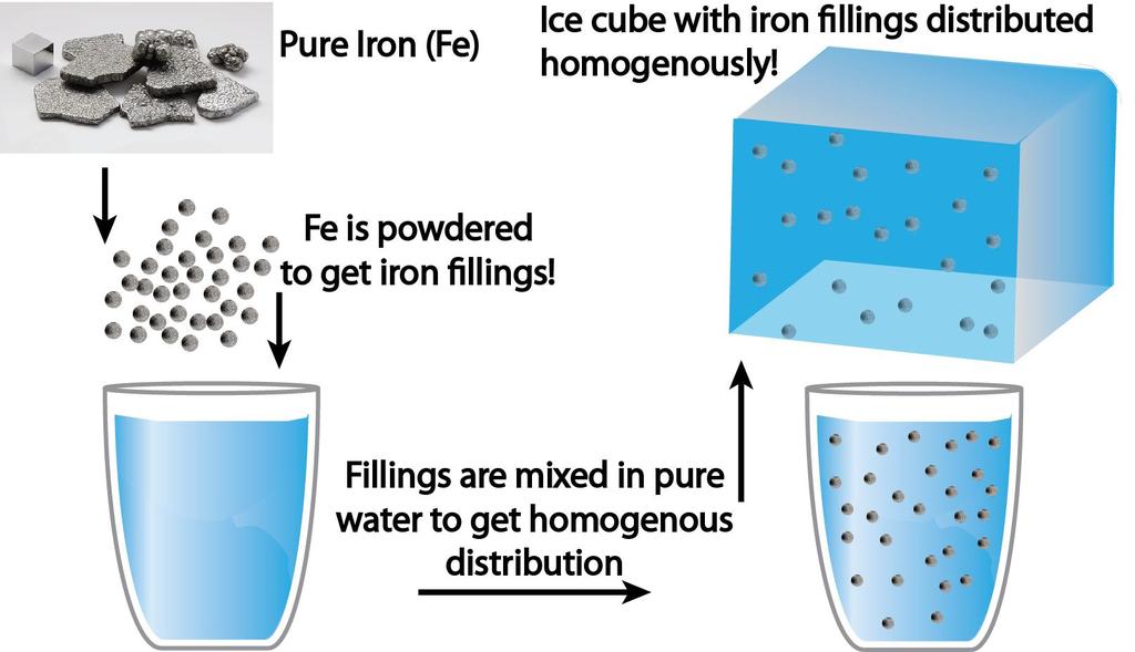
6 An Experiment! 6
 ice cube??? 7")
7 Will the magnet move (magnetic) ice cube??? 7
 Semiconductor!")
8 (Magnetic) Ice cube = (Magnetic) Semiconductor!!! 8

9 Importance of magnetic ions 9
10 10
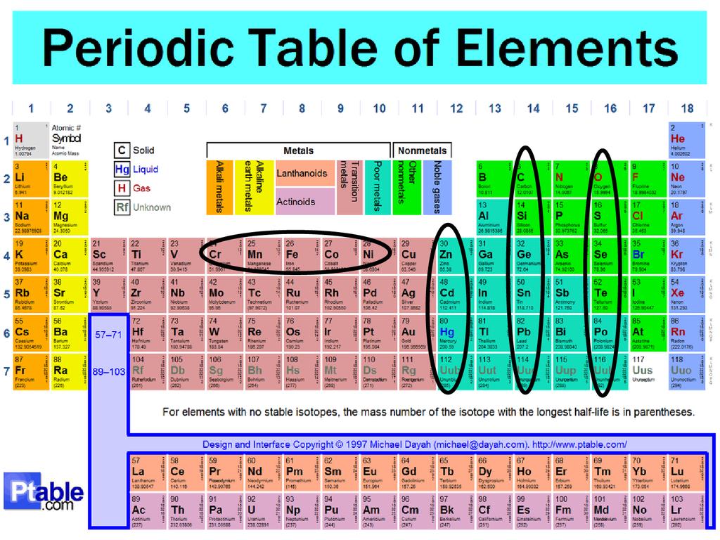
11 Materials for DMS II VI II-VI Transition Metal Zn S ZnS Mn or Fe or Co Cd Te CdTe Mn or Fe or Co Cd Se CdSe Mn or Fe or Co IV VI IV-VI Transition Metal Pb Se PbSe Mn or Fe or Co Sn Te SnTe Mn or Fe or Co V VI V-VI Transition Metal Ga As GaAs Mn or Fe or Co In Sb InSb Mn or Fe or Co 11

12 Formation of DMS 12
13 Aspects of DMS Coexistence and interaction of two different electronic sub systems: delocalized conduction (s-type) and valence (p-type) band electrons and localized (d or f-type) electrons of magnetic ions. The spd exchange interaction leads to strong band splitting, which result in giant magneto optical effects The solubility limit of magnetic elements in III-V semiconductors is very low, but in order to have ferromagnetism in DMS, a sizable amount of magnetic ions are needed. The highest conclusively reported Tc of DMS is around 110 K for 5 % doped GaAs. 13
14 Applications of DMS Charge and spin degrees of freedom accommodated into a single material exhibits interesting magnetic, magneto-optical, magnetoelectronic and other properties An inherent advantage of magnetoelectronics over electronics is the fact that magnet tend to stay magnetized for long. DMS materials are very attractive for integration of photonic (lightemitting diodes), electronic (field effect transistors), and magnetic (memory) devices on a single substrate 14
15 Some important application areas of DMS Photonics plus spintronics (Spin+electronics = Spintronics) Improved spin transistor Transistors spin toward quantum computing Magnetic spins to store quantum information Microscope to view magnetism at atomic level Ballistic magneto resistance Missile guidance Fast accurate position and motion sensing of mechanical components in precision engineering and in robotics In automotive sensors 15


16 16
EXTRINSIC SEMICONDUCTOR
 EXTRINSIC SEMICONDUCTOR In an extrinsic semiconducting material, the charge carriers originate from impurity atoms added to the original material is called impurity [or] extrinsic semiconductor. This Semiconductor
SIMULATIONS ON DILUTE MAGNETIC SEMICONDUCTOR PROPERTIES
 Romanian Reports in Physics, Vol. 62, No. 1, P. 115 120, 2010 SIMULATIONS ON DILUTE MAGNETIC SEMICONDUCTOR PROPERTIES M. NEGOITA, E. A. PATROI, C. V. ONICA National Institute for Research and Development
Semiconductors. SEM and EDAX images of an integrated circuit. SEM EDAX: Si EDAX: Al. Institut für Werkstoffe der ElektrotechnikIWE
 SEM and EDAX images of an integrated circuit SEM EDAX: Si EDAX: Al source: [Cal 99 / 605] M&D-.PPT, slide: 1, 12.02.02 Classification semiconductors electronic semiconductors mixed conductors ionic conductors
Material Science II. d Electron systems
 Material Science II. d Electron systems 1. Electronic structure of transition-metal ions (May 23) 2. Crystal structure and band structure (June 13) 3. Mott s (June 20) 4. Metal- transition (June 27) 5.
Chapter 1 Overview of Semiconductor Materials and Physics
 Chapter 1 Overview of Semiconductor Materials and Physics Professor Paul K. Chu Conductivity / Resistivity of Insulators, Semiconductors, and Conductors Semiconductor Elements Period II III IV V VI 2 B
CME 300 Properties of Materials. ANSWERS: Homework 9 November 26, As atoms approach each other in the solid state the quantized energy states:
 CME 300 Properties of Materials ANSWERS: Homework 9 November 26, 2011 As atoms approach each other in the solid state the quantized energy states: are split. This splitting is associated with the wave
Research Highlights. Salient results from our group. Mixed phosphides in Sn-P and Sn-Mn-P systems
 Research Highlights Dilute magnetic semiconductors and Spintronics Spintronics is a branch of electronics emerged from the dilute magnetic semiconductor in an aspect of utilization of the spin in addition
Ga and P Atoms to Covalent Solid GaP
 Ga and P Atoms to Covalent Solid GaP Band Gaps in Binary Group III-V Semiconductors Mixed Semiconductors Affect of replacing some of the As with P in GaAs Band Gap (ev) (nm) GaAs 1.35 919 (IR) GaP 2.24
EECS143 Microfabrication Technology
 EECS143 Microfabrication Technology Professor Ali Javey Introduction to Materials Lecture 1 Evolution of Devices Yesterday s Transistor (1947) Today s Transistor (2006) Why Semiconductors? Conductors e.g
Electrical spin-injection into semiconductors
 Electrical spin-injection into semiconductors L. W. Molenkamp Physikalisches Institut Universität Würzburg Am Hubland 97074 Würzburg Germany Contents Motivation The usual approach Theoretical treatment
smal band gap Saturday, April 9, 2011
 small band gap upper (conduction) band empty small gap valence band filled 2s 2p 2s 2p hybrid (s+p)band 2p no gap 2s (depend on the crystallographic orientation) extrinsic semiconductor semi-metal electron
Semiconductors and Optoelectronics. Today Semiconductors Acoustics. Tomorrow Come to CH325 Exercises Tours
 Semiconductors and Optoelectronics Advanced Physics Lab, PHYS 3600 Don Heiman, Northeastern University, 2017 Today Semiconductors Acoustics Tomorrow Come to CH325 Exercises Tours Semiconductors and Optoelectronics
5 Magnetic Sensors Introduction Theory. Applications
 Sensor devices Magnetic sensors Outline 5 Magnetic Sensors Introduction Theory GalvanomagneticG Effects Applications Introduction A magnetic sensor is a transducer that converts a magnetic field into an
VALLIAMMAI ENGINEERING COLLEGE
 VALLIAMMAI ENGINEERING COLLEGE SRM Nagar, Kattankulathur 603 203 DEPARTMENT OF PHYSICS QUESTION BANK II SEMESTER PH8252 - PHYSICS FOR INFORMATION SCIENCE (Common to CSE & IT) Regulation 2017 Academic Year
EE143 Fall 2016 Microfabrication Technologies. Evolution of Devices
 EE143 Fall 2016 Microfabrication Technologies Prof. Ming C. Wu wu@eecs.berkeley.edu 511 Sutardja Dai Hall (SDH) 1-1 Evolution of Devices Yesterday s Transistor (1947) Today s Transistor (2006) 1-2 1 Why
THE STUDY OF ANTIFERROMAGNETISM IN DILUTED MAGNETIC SEMICONDUCTOR CDMNTE
 THE STUDY OF ANTIFERROMAGNETISM IN DILUTED MAGNETIC SEMICONDUCTOR CDMNTE By Gebru Tadesse A THESIS PRESENTED TO THE SCHOOL OF GRADUATE STUDIES ADDIS ABABA UNIVERSITY IN PARTIAL FULFILLMENT OF THE REQUIREMENTS
2005 EDP Sciences. Reprinted with permission.
 H. Holmberg, N. Lebedeva, S. Novikov, J. Ikonen, P. Kuivalainen, M. Malfait, and V. V. Moshchalkov, Large magnetoresistance in a ferromagnetic GaMnAs/GaAs Zener diode, Europhysics Letters 71 (5), 811 816
Making Semiconductors Ferromagnetic: Opportunities and Challenges
 Making Semiconductors Ferromagnetic: Opportunities and Challenges J.K. Furdyna University of Notre Dame Collaborators: X. Liu and M. Dobrowolska, University of Notre Dame T. Wojtowicz, Institute of Physics,
DOI: /jacs.7b02953 J. Am. Chem. Soc. 2017, 139,
 DOI: 10.1021/jacs.7b02953 J. Am. Chem. Soc. 2017, 139, 6761 6770 Manju C K 01.07.2017 Introduction In the last several decades, colloidal chemistry has provided effective ways to synthesize inorganic nanomaterials
Lecture 20: Semiconductor Structures Kittel Ch 17, p , extra material in the class notes
 Lecture 20: Semiconductor Structures Kittel Ch 17, p 494-503, 507-511 + extra material in the class notes MOS Structure Layer Structure metal Oxide insulator Semiconductor Semiconductor Large-gap Semiconductor
Spintronics. Seminar report SUBMITTED TO: SUBMITTED BY:
 A Seminar report On Spintronics Submitted in partial fulfillment of the requirement for the award of degree of Electronics SUBMITTED TO: SUBMITTED BY: www.studymafia.org www.studymafia.org Preface I have
Classification of Solids
 Classification of Solids Classification by conductivity, which is related to the band structure: (Filled bands are shown dark; D(E) = Density of states) Class Electron Density Density of States D(E) Examples
Fundamental concepts of spintronics
 Fundamental concepts of spintronics Jaroslav Fabian Institute for Theoretical Physics University of Regensburg Stara Lesna, 24. 8. 2008 SFB 689 :outline: what is spintronics? spin injection spin-orbit
Introductory Nanotechnology ~ Basic Condensed Matter Physics ~
 Introductory Nanotechnology ~ Basic Condensed Matter Physics ~ Atsufumi Hirohata Department of Electronics Quick Review over the Last Lecture Classic model : Dulong-Petit empirical law c V, mol 3R 0 E
ELECTRONIC DEVICES AND CIRCUITS SUMMARY
 ELECTRONIC DEVICES AND CIRCUITS SUMMARY Classification of Materials: Insulator: An insulator is a material that offers a very low level (or negligible) of conductivity when voltage is applied. Eg: Paper,
Author : Fabrice BERNARD-GRANGER September 18 th, 2014
 Author : September 18 th, 2014 Spintronic Introduction Spintronic Design Flow and Compact Modelling Process Variation and Design Impact Semiconductor Devices Characterisation Seminar 2 Spintronic Introduction
Most matter is electrically neutral; its atoms and molecules have the same number of electrons as protons.
 Magnetism Electricity Magnetism Magnetic fields are produced by the intrinsic magnetic moments of elementary particles associated with a fundamental quantum property, their spin. -> permanent magnets Magnetic
Lecture 9: Metal-semiconductor junctions
 Lecture 9: Metal-semiconductor junctions Contents 1 Introduction 1 2 Metal-metal junction 1 2.1 Thermocouples.......................... 2 3 Schottky junctions 4 3.1 Forward bias............................
Semiconductor Spintronics
 IEEE TRANSACTIONS ON NANOTECHNOLOGY, VOL. 1, NO. 1, MARCH 2002 19 Semiconductor Spintronics Hiro Akinaga and Hideo Ohno, Member, IEEE Abstract We review recent progress made in the field of semiconductor
Giant Magnetoresistance
 Giant Magnetoresistance This is a phenomenon that produces a large change in the resistance of certain materials as a magnetic field is applied. It is described as Giant because the observed effect is
Challenges for Materials to Support Emerging Research Devices
 Challenges for Materials to Support Emerging Research Devices C. Michael Garner*, James Hutchby +, George Bourianoff*, and Victor Zhirnov + *Intel Corporation Santa Clara, CA + Semiconductor Research Corporation
A spin Esaki diode. Makoto Kohda, Yuzo Ohno, Koji Takamura, Fumihiro Matsukura, and Hideo Ohno. Abstract
 A spin Esaki diode Makoto Kohda, Yuzo Ohno, Koji Takamura, Fumihiro Matsukura, and Hideo Ohno Laboratory for Electronic Intelligent Systems, Research Institute of Electrical Communication, Tohoku University,
Nano physics for semiconductors, great challenge
 Nano physics for semiconductors, great challenge Oleksandr Voskoboynikov 霍斯科 Phone: ext. 54174 Office: 646 ED bld.4 E-mail: vam@faculty.nctu.edu.tw Web: http://www.cc.nctu.edu.tw/~vam In collaboration
Department of Electrical Engineering and Information Systems, Tanaka-Ohya lab.
 Observation of the room-temperature local ferromagnetism and its nanoscale expansion in the ferromagnetic semiconductor Ge 1 xfe x Yuki K. Wakabayashi 1 and Yukio Takahashi 2 1 Department of Electrical
Review of Semiconductor Physics. Lecture 3 4 Dr. Tayab Din Memon
 Review of Semiconductor Physics Lecture 3 4 Dr. Tayab Din Memon 1 Electronic Materials The goal of electronic materials is to generate and control the flow of an electrical current. Electronic materials
Ferroelectric Field Effect Transistor Based on Modulation Doped CdTe/CdMgTe Quantum Wells
 Vol. 114 (2008) ACTA PHYSICA POLONICA A No. 5 Proc. XXXVII International School of Semiconducting Compounds, Jaszowiec 2008 Ferroelectric Field Effect Transistor Based on Modulation Doped CdTe/CdMgTe Quantum
Injection of Optically Generated Spins through Magnetic/Nonmagnetic Heterointerface: Ruling out Possible Detection Artifacts
 Vol. 106 (2004) ACTA PHYSICA POLONICA A No. 2 Proceedings of the XXXIII International School of Semiconducting Compounds, Jaszowiec 2004 Injection of Optically Generated Spins through Magnetic/Nonmagnetic
4. I-V characteristics of electric
 KL 4. - characteristics of electric conductors 4.1 ntroduction f an electric conductor is connected to a voltage source with voltage a current is produced. We define resistance being the ratio of the voltage
EE 5344 Introduction to MEMS CHAPTER 5 Radiation Sensors
 EE 5344 Introduction to MEMS CHAPTER 5 Radiation Sensors 5. Radiation Microsensors Radiation µ-sensors convert incident radiant signals into standard electrical out put signals. Radiant Signals Classification
FACULTY OF ENGINEERING ALEXANDRIA UNVERSITY. Solid State lab. Instructors Dr. M. Ismail El-Banna Dr. Mohamed A. El-Shimy TA Noha Hanafy
 FACULTY OF ENGINEERING ALEXANDRIA UNVERSITY Solid State lab Instructors Dr. M. Ismail El-Banna Dr. Mohamed A. El-Shimy TA Noha Hanafy 2017-2018 first term A. Experiments 1- Relationship between the intensity
Advances in wide bandgap materials for semiconductor spintronics
 Materials Science and Engineering R 40 (2003) 137 168 Advances in wide bandgap materials for semiconductor spintronics S.J. Pearton 1,*, C.R. Abernathy 1, D.P. Norton 1, A.F. Hebard 2, Y.D. Park 3, L.A.
HALL EFFECT IN SEMICONDUCTORS
 Warsaw University of Technology Faculty of Physics Physics Laboratory I P Andrzej Kubiaczyk 30 HALL EFFECT IN SEMICONDUCTORS 1. ackground 1.1. Electron motion in electric and magnetic fields A particle
* motif: a single or repeated design or color
 Chapter 2. Structure A. Electronic structure vs. Geometric structure B. Clean surface vs. Adsorbate covered surface (substrate + overlayer) C. Adsorbate structure - how are the adsorbed molecules bound
TRANSVERSE SPIN TRANSPORT IN GRAPHENE
 International Journal of Modern Physics B Vol. 23, Nos. 12 & 13 (2009) 2641 2646 World Scientific Publishing Company TRANSVERSE SPIN TRANSPORT IN GRAPHENE TARIQ M. G. MOHIUDDIN, A. A. ZHUKOV, D. C. ELIAS,
From Hall Effect to TMR
 From Hall Effect to TMR 1 Abstract This paper compares the century old Hall effect technology to xmr technologies, specifically TMR (Tunnel Magneto-Resistance) from Crocus Technology. It covers the various
Spintronics at Nanoscale
 Colloquium@NTHU Sep 22, 2004 Spintronics at Nanoscale Hsiu-Hau Lin Nat l Tsing-Hua Univ & Nat l Center for Theoretical Sciences What I have been doing Spintronics: Green s function theory for diluted magnetic
A Review of Spintronics based Data Storage. M.Tech Student Professor
 A Review of Spintronics based Data Storage By: Mohit P. Tahiliani S. Vadakkan M.Tech Student Professor NMAMIT, Nitte NMAMIT, Nitte CONTENTS Introduction Giant Magneto Resistance (GMR) Tunnel Magneto Resistance
Chap. 1 (Introduction), Chap. 2 (Components and Circuits)
, Chap. 2 (Components and Circuits)") CHEM 455 The class describes the principles and applications of modern analytical instruments. Emphasis is placed upon the theoretical basis of each type of instrument, its optimal area of application,
CHEM 455 The class describes the principles and applications of modern analytical instruments. Emphasis is placed upon the theoretical basis of each type of instrument, its optimal area of application,
Mon., Feb. 04 & Wed., Feb. 06, A few more instructive slides related to GMR and GMR sensors
 Mon., Feb. 04 & Wed., Feb. 06, 2013 A few more instructive slides related to GMR and GMR sensors Oscillating sign of Interlayer Exchange Coupling between two FM films separated by Ruthenium spacers of
Lecture 20 - Semiconductor Structures
 Lecture 0: Structures Kittel Ch 17, p 494-503, 507-511 + extra material in the class notes MOS Structure metal Layer Structure Physics 460 F 006 Lect 0 1 Outline What is a semiconductor Structure? Created
Lecture 3: Semiconductors and recombination. Prof Ken Durose, University of Liverpool
 Lecture 3: Semiconductors and recombination Prof Ken Durose, University of Liverpool Outline semiconductors and 1. Band gap representations 2. Types of semiconductors -Adamantine semiconductors (Hume -Rothery
Conductivity and Semi-Conductors
 Conductivity and Semi-Conductors J = current density = I/A E = Electric field intensity = V/l where l is the distance between two points Metals: Semiconductors: Many Polymers and Glasses 1 Electrical Conduction
Harvesting Heat through Seebeck Spin Tunneling Effect
 Harvesting Heat through Seebeck Spin Tunneling Effect Costel Constantin James Madison University Science Enabled by Photon Source, May 2012 Outline 1. Spintronics vs. Spin Caloritronics. 2. Novel Spin
Type of material Numbers of FREE electrons Resitsivity/ resitance Insulator LOW HIGH Semi-Conductor MEDIUM MEDIUM Conductor HIGH LOW
 9.4.3 2 (i) Identify that some electrons in solids are shared between atoms and move freely There are three main ways in which matter is held together. They all involve the valence or outer shell electrons.
Introduction to Engineering Materials ENGR2000. Dr.Coates
 Introduction to Engineering Materials ENGR2000 Chapter 18: Electrical Properties Dr.Coates 18.2 Ohm s Law V = IR where R is the resistance of the material, V is the voltage and I is the current. l R A
Chapter 4: Bonding in Solids and Electronic Properties. Free electron theory
 Chapter 4: Bonding in Solids and Electronic Properties Free electron theory Consider free electrons in a metal an electron gas. regards a metal as a box in which electrons are free to move. assumes nuclei
Contents. Acknowledgments
 MAGNETIC MATERIALS Fundamentals and Applications Second edition NICOLA A. SPALDIN University of California, Santa Barbara CAMBRIDGE UNIVERSITY PRESS Contents Acknowledgments page xiii I Basics 1 Review
Semiconductors. Semiconductors also can collect and generate photons, so they are important in optoelectronic or photonic applications.
 Semiconductors Semiconducting materials have electrical properties that fall between true conductors, (like metals) which are always highly conducting and insulators (like glass or plastic or common ceramics)
Semiconductor Devices, Fall Gunnar Malm, Associate Professor Integrated Devices and Circuits, Kista Campus
 Semiconductor Devices, Fall 2014 Gunnar Malm, Associate Professor Integrated Devices and Circuits, Kista Campus gunta@kth.se, 08-790 4332 Semiconductor procesing at KTH Electrum Laboratory Stepper Lithography
Basic cell design. Si cell
 Basic cell design Si cell 1 Concepts needed to describe photovoltaic device 1. energy bands in semiconductors: from bonds to bands 2. free carriers: holes and electrons, doping 3. electron and hole current:
Cover Page. The handle holds various files of this Leiden University dissertation
 Cover Page The handle http://hdl.handle.net/1887/24306 holds various files of this Leiden University dissertation Author: Verhagen, T.G.A. Title: Magnetism and magnetization dynamics in thin film ferromagnets
Quantum Phenomena & Nanotechnology (4B5)
") Quantum Phenomena & Nanotechnology (4B5) The 2-dimensional electron gas (2DEG), Resonant Tunneling diodes, Hot electron transistors Lecture 11 In this lecture, we are going to look at 2-dimensional electron
Quantum Phenomena & Nanotechnology (4B5) The 2-dimensional electron gas (2DEG), Resonant Tunneling diodes, Hot electron transistors Lecture 11 In this lecture, we are going to look at 2-dimensional electron
CHAPTER 2 MAGNETISM. 2.1 Magnetic materials
 CHAPTER 2 MAGNETISM Magnetism plays a crucial role in the development of memories for mass storage, and in sensors to name a few. Spintronics is an integration of the magnetic material with semiconductor
Engineering 2000 Chapter 8 Semiconductors. ENG2000: R.I. Hornsey Semi: 1
 Engineering 2000 Chapter 8 Semiconductors ENG2000: R.I. Hornsey Semi: 1 Overview We need to know the electrical properties of Si To do this, we must also draw on some of the physical properties and we
Current mechanisms Exam January 27, 2012
 Current mechanisms Exam January 27, 2012 There are four mechanisms that typically cause currents to flow: thermionic emission, diffusion, drift, and tunneling. Explain briefly which kind of current mechanisms
Lecture 1 - Electrons, Photons and Phonons. September 4, 2002
 6.720J/3.43J - Integrated Microelectronic Devices - Fall 2002 Lecture 1-1 Lecture 1 - Electrons, Photons and Phonons Contents: September 4, 2002 1. Electronic structure of semiconductors 2. Electron statistics
Using Light to Prepare and Probe an Electron Spin in a Quantum Dot
 A.S. Bracker, D. Gammon, E.A. Stinaff, M.E. Ware, J.G. Tischler, D. Park, A. Shabaev, and A.L. Efros Using Light to Prepare and Probe an Electron Spin in a Quantum Dot A.S. Bracker, D. Gammon, E.A. Stinaff,
Resistance (R) Temperature (T)
 Temperature (T)") CHAPTER 1 Physical Properties of Elements and Semiconductors 1.1 Introduction Semiconductors constitute a large class of substances which have resistivities lying between those of insulators and conductors.
CHAPTER 1 Physical Properties of Elements and Semiconductors 1.1 Introduction Semiconductors constitute a large class of substances which have resistivities lying between those of insulators and conductors.
SUPPLEMENTARY INFORMATION
 Dirac electron states formed at the heterointerface between a topological insulator and a conventional semiconductor 1. Surface morphology of InP substrate and the device Figure S1(a) shows a 10-μm-square
Exchange interactions
 Exchange interactions Tomasz Dietl Institute of Physics, Polish Academy of Sciences, PL-02-668Warszawa, Poland Institute of Theoretical Physics, University of Warsaw, PL-00-681Warszawa, Poland 1. POTENTIAL
Advantages / Disadvantages of semiconductor detectors
 Advantages / Disadvantages of semiconductor detectors Semiconductor detectors have a high density (compared to gas detector) large energy loss in a short distance diffusion effect is smaller than in gas
Lecture 3: Heterostructures, Quasielectric Fields, and Quantum Structures
 Lecture 3: Heterostructures, Quasielectric Fields, and Quantum Structures MSE 6001, Semiconductor Materials Lectures Fall 2006 3 Semiconductor Heterostructures A semiconductor crystal made out of more
New magnetic materials for Spintronics
 ew magnetic materials for Spintronics Juana Moreno utline What is spintronics? And why? Ferromagnetic semiconductors rganic magnets What is spintronics? And why? Spin-unpolarized current: Electrons move
THE STUDY OF FERRO AND ANTIFERROMAGNETISM IN. DILUTED MAGNETIC SEMICONDUCTOR GaMnAs
 THE STUDY OF FERRO AND ANTIFERROMAGNETISM IN DILUTED MAGNETIC SEMICONDUCTOR GaMnAs A thesis submitted to the School of Graduate Studies Addis Ababa University In partial Fulfillment of the Requirements
Electronic Properties of Lead Telluride Quantum Wells
 Electronic Properties of Lead Telluride Quantum Wells Liza Mulder Smith College 2013 NSF/REU Program Physics Department, University of Notre Dame Advisors: Profs. Jacek Furdyna, Malgorzata Dobrowolska,
Challenges and Opportunities. Prof. J. Raynien Kwo 年
 Nanoelectronics Beyond Si: Challenges and Opportunities Prof. J. Raynien Kwo 年 立 Si CMOS Device Scaling Beyond 22 nm node High κ,, Metal gates, and High mobility channel 1947 First Transistor 1960 1960
 lectures accompanying the book: Solid State Physics: An Introduction, by Philip ofmann (2nd edition 2015, ISBN-10: 3527412824, ISBN-13: 978-3527412822, Wiley-VC Berlin. www.philiphofmann.net 1 Bonds between
Advanced Topics In Solid State Devices EE290B. Will a New Milli-Volt Switch Replace the Transistor for Digital Applications?
 Advanced Topics In Solid State Devices EE290B Will a New Milli-Volt Switch Replace the Transistor for Digital Applications? August 28, 2007 Prof. Eli Yablonovitch Electrical Engineering & Computer Sciences
Universal valence-band picture of. the ferromagnetic semiconductor GaMnAs
 Universal valence-band picture of the ferromagnetic semiconductor GaMnAs Shinobu Ohya *, Kenta Takata, and Masaaki Tanaka Department of Electrical Engineering and Information Systems, The University of
We have arrived to the question: how do molecular bonds determine the band gap? We have discussed that the silicon atom has four outer electrons.
 ET3034Tux - 2.2.2 - Band Gap 2 - Electrons in Molecular Bonds We have arrived to the question: how do molecular bonds determine the band gap? We have discussed that the silicon atom has four outer electrons.
EXCHANGE INTERACTIONS: SUPER-EXCHANGE, DOUBLE EXCHANGE, RKKY; MAGNETIC ORDERS. Tomasz Dietl
 Analele Universităţii de Vest din Timişoara Vol. LIII, 2009 Seria Fizică EXCHANGE INTERACTIONS: SUPER-EXCHANGE, DOUBLE EXCHANGE, RKKY; MAGNETIC ORDERS Tomasz Dietl Institute of Physics, Polish Academy
Electrical Characterization with SPM Application Modules
 Electrical Characterization with SPM Application Modules Metrology, Characterization, Failure Analysis: Data Storage Magnetoresistive (MR) read-write heads Semiconductor Transistors Interconnect Ferroelectric
EECS130 Integrated Circuit Devices
 EECS130 Integrated Circuit Devices Professor Ali Javey 8/30/2007 Semiconductor Fundamentals Lecture 2 Read: Chapters 1 and 2 Last Lecture: Energy Band Diagram Conduction band E c E g Band gap E v Valence
N. Gonzalez Szwacki and Jacek A. Majewski Faculty of Physics, University of Warsaw, ul. Hoża 69, Warszawa, Poland
 Ab initio studies of Co 2 FeAl 1-x Si x Heusler alloys N. Gonzalez Szwacki and Jacek A. Majewski Faculty of Physics, University of Warsaw, ul. Hoża 69, 00-681 Warszawa, Poland Abstract We present results
Recent developments in spintronic
 Recent developments in spintronic Tomas Jungwirth nstitute of Physics ASCR, Prague University of Nottingham in collaboration with Hitachi Cambridge, University of Texas, Texas A&M University - Spintronics
From magnetic polarons to magnetic quantum dots. Jacek Kossut, Institute of Physics of the Polish Academy of Sciences
 From magnetic polarons to magnetic quantum dots Jacek Kossut, Institute of Physics of the Polish Academy of Sciences 1 Diluted magnetic semiconductors Magnetic Polarons Self-assembled dots of CdMnTe: Formation
Semiconductor Fundamentals. Professor Chee Hing Tan
 Semiconductor Fundamentals Professor Chee Hing Tan c.h.tan@sheffield.ac.uk Why use semiconductor? Microprocessor Transistors are used in logic circuits that are compact, low power consumption and affordable.
2D MBE Activities in Sheffield. I. Farrer, J. Heffernan Electronic and Electrical Engineering The University of Sheffield
 2D MBE Activities in Sheffield I. Farrer, J. Heffernan Electronic and Electrical Engineering The University of Sheffield Outline Motivation Van der Waals crystals The Transition Metal Di-Chalcogenides
Lecture 2. Semiconductor Physics. Sunday 4/10/2015 Semiconductor Physics 1-1
 Lecture 2 Semiconductor Physics Sunday 4/10/2015 Semiconductor Physics 1-1 Outline Intrinsic bond model: electrons and holes Charge carrier generation and recombination Intrinsic semiconductor Doping:
Minimal Update of Solid State Physics
 Minimal Update of Solid State Physics It is expected that participants are acquainted with basics of solid state physics. Therefore here we will refresh only those aspects, which are absolutely necessary
Supplementary Figure 1: Spin noise spectra of 55 Mn in bulk sample at BL =10.5 mt, before subtraction of the zero-frequency line. a, Contour plot of
 1 Supplementary Figure 1: Spin noise spectra of 55 Mn in bulk sample at BL =10.5 mt, before subtraction of the zero-frequency line. a, Contour plot of the spin noise spectra calculated with Eq. (2) for
Electron Energy, E E = 0. Free electron. 3s Band 2p Band Overlapping energy bands. 3p 3s 2p 2s. 2s Band. Electrons. 1s ATOM SOLID.
 Electron Energy, E Free electron Vacuum level 3p 3s 2p 2s 2s Band 3s Band 2p Band Overlapping energy bands Electrons E = 0 1s ATOM 1s SOLID In a metal the various energy bands overlap to give a single
Calculating Band Structure
 Calculating Band Structure Nearly free electron Assume plane wave solution for electrons Weak potential V(x) Brillouin zone edge Tight binding method Electrons in local atomic states (bound states) Interatomic
The Electromagnetic Properties of Materials
 The lectromagnetic Properties of Materials lectrical conduction Metals Semiconductors Insulators (dielectrics) Superconductors Magnetic materials Ferromagnetic materials Others Photonic Materials (optical)
SUPPLEMENTARY INFORMATION
 doi:10.1038/nature12036 We provide in the following additional experimental data and details on our demonstration of an electrically pumped exciton-polariton laser by supplementing optical and electrical
UNIT - IV SEMICONDUCTORS AND MAGNETIC MATERIALS
 1. What is intrinsic If a semiconductor is sufficiently pure, then it is known as intrinsic semiconductor. ex:: pure Ge, pure Si 2. Mention the expression for intrinsic carrier concentration of intrinsic
Lecture 7: Extrinsic semiconductors - Fermi level
 Lecture 7: Extrinsic semiconductors - Fermi level Contents 1 Dopant materials 1 2 E F in extrinsic semiconductors 5 3 Temperature dependence of carrier concentration 6 3.1 Low temperature regime (T < T
Emerging spintronics-based logic technologies
 Center for Spintronic Materials, Interfaces, and Novel Architectures Emerging spintronics-based logic technologies Zhaoxin Liang Meghna Mankalale Jian-Ping Wang Sachin S. Sapatnekar University of Minnesota
ACII-Part II: Structure of solids; Structure-properties relationship
 ACII-Part II: Structure of solids; Structure-properties relationship Dr. Liliana Viciu ACII: Prof. Reinhard Nesper and Dr. Liliana Viciu 1 Liliana Viciu B. Sc. and M.Sc. at University of Bucharest, Romania
Introduction to Optoelectronic Device Simulation by Joachim Piprek
 NUSOD 5 Tutorial MA Introduction to Optoelectronic Device Simulation by Joachim Piprek Outline:. Introduction: VCSEL Example. Electron Energy Bands 3. Drift-Diffusion Model 4. Thermal Model 5. Gain/Absorption