Special Topics in Semiconductor Nanotechnology ECE 598XL
|
|
|
- Austen Phillips
- 5 years ago
- Views:
Transcription
1 Special Topics in Semiconductor Nanotechnology ECE 598XL Fall 2009
2 ECE 598XL Syllabus Overview: size matters Formation Process Characterization SOA device applications and potentials Homework or quizzes every 1-2 weeks Exams Mid-term: Wikipedia entry - literature search report on a topic (4 5 pages) Final: proposal Group project ( 2 4 students self-assembled) pages total Grades 30% HW, 30% Mid-term, and 40% Final
3 Topics Examples # of lectures 1. Introduction of nanotechnology 1 2. Formation process of various nanotechnology building blocks 9 Self-assembled quantum dots and anti-dots 1 Patterned and templated growth 1 Bottom-up: Epitaxial growth (MOCVD, MBE, etc.) VLS nanowires (highly anisotropic growth) 2 Top-down: lithography and etching SAE nanowires (highly hl anisotropic i growth) 2 Combination of bottom-up and top-down 2 Surface passivation ALD, wet-chemical, etc. 1
4 3. Characterization of various nanotechnology building blocks 4 Structural morphology, orientation, crystallinity, strain, compliance, and defects SEM, TEM, AFM, STM, X-ray, EBIC 0.5 Chemical composition and impurity SIMS, EDS, EELS, Auger, XPS 1 Optical PL, CL, RAMAN, NSOM, time resolved pump-probe 2 Electrical IV, CV, conductive AFM, STM 0.5 Midterm exam 1 4. Nano-devices 9 for light emission and detection Nanowire waveguide, LEDs and lasers 2 Nanotube resonators 1 Nanowire detectors 1 for energy conversion Nanowire photovoltaic 1 Nanowire thermoelectric devices 1 for extending IC roadmap Nanowire and nanotube finfet etc. 1 for sensing Resonator and transistor based etc. 1 misc. Nanofluidics etc Nano-systems and manufacturing field induced d assembly, dry transfer printing etc. 1
5 Books Texts: class notes and journal papers. p Reference books (partial list): Handbook of Semiconductors and Nanodevices, by Balandin and Wang, 2006 (in reference section in Grainger) Epitaxy of nanostructures, By Shchukin, Ledentsov, Bimberg, Springer, 2004 Semiconductor Nanostructures for Optoelectronic Applications, By Steiner, Artech House, 2004 Future Trends in Microelectronics, by Luryi, Xu, Zaslavsky, John Wiley & Sons, 2007

, colloidal chemistry")

6 Introduction to Nanotechnology The definition and who owns it? Chemists and Biologists: i atoms (3Å), DNA (2 nm), colloidal chemistry Engineers: QW laser, nano-transistors t The facts and the hype Feynman There is plenty of room at the bottom Drexler


7 Engineering village search Nano: 158, 499 Nanotechnology: 118,349 Nanowire: 31,205 Quantum Dots: 61,753 Popular Press Scientific Journals targeting Nano specifically Nature Nanotechnology Nano Letters ACS Nano Nanotechnology Small IEEE Transactions on Nanotechnology Facts and Hype
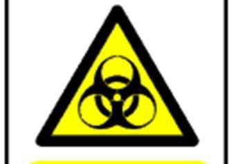


8 Nanomaterial Safety Plan Nanomaterials Might Be Present
9 Semiconductor bandgap Direct band gap High mobility Versatile heterojunction EMF ltd Bandgap Ener rgy (ev) AlAs Lattice Constant (Å)
10 Nanotechnology Overview SIZE MATTERS new kinds of forces and new kinds of possibilities, new kinds of effects. When we get to the very, very small world say circuits of seven atoms---we have a lot of new things that would happen that represent completely new opportunities for design. Atoms on a small scale behave like nothing on a large scale, for they satisfy the laws of quantum mechanics. So, as we go down and fiddle around with the atoms down there, we are working with different laws, and we can expect to do different things. We can manufacture in different ways. We can use, not just circuits, but some system involving the quantized energy levels, or the interactions of quantized spins, etc. Richard Feynman, December 1959


11 Electronic Properties vs Size Quantization of Density of States Ev and Ec split into overlapping subbands - successively narrower as the e- motion is restricted in more dimensions Saleh and Teich, Fundamentals of Photonics, Ch.15
12 Electronic Properties vs Size Quantum confinement ΔΕ g Particle-in-a-box approximation Shape dependence Buhro and Colvin, Nature Materials, 2, 138 (2003)
13 Electronic Properties vs Size QDs: colloidal nanocrystals CdSe quantum dots that are increasing in size (left to right). Optical absorption spectra of CdSe nanocrystals dispersed in hexane and corresponding TEM avg. size distribution ( Å). J. Am. Chem. Soc., 115, 8706 (1993)

14 Electronic Properties vs Size Quantum Well Lasers QW in most commercial diode lasers Quantum size effect discrete energy level constant DOS at each step Lower threshold Narrow linewidthidth Temperature stability Holonyak, 1980
.")
15 Mechanical Properties vs Size Young s Modulus Engineering single crystal ZnO nanotube wall thickness Nanotechnology, 19, (2008). Single crystal ZnO nanowire diameter PRL, 96, (2006). Single crystal Si thickness APL, 83, 3083 (2003). polycrystalline Pd film thickness Thin Solid Films, 492, 166 (2005) polycrystalline Cr film thickness APL, 85, 3555 (2004) CNT diameter Science 283, 1511 (1999).


.")
16 Mechanical Properties vs Size Effect of Twin Boundaries in Cu films 100 nm 2 n m Coherent twin boundaries are effective grain boundaries in strengthening materials Strengthening Cu when high densities of nm thick twins are introduced in subum sized grains. Below 15 nm twin thickness, Cu starts to soften. Two competing mechanism for hardening: dislocation-dislocation interaction in coarse twins Dislocation- twin boundary hardening in fine twins Revealing the Maximum Strength in Nanotwinned Copper, L Lu et al. Science 323, 607 (2009). Strength and ductility of nano-twinned materials L. Lu, K. Lu, et al, Science, 2004
 scattering")


17 Electrical Properties vs Size Surface/interface effect on Resistivity Carrier scattering: Impurity (Coulomb) scattering (donors/acceptors): µ=t 3/2 /N i Lattice scattering (phonons): GaAs µ e T -1 ; µ h T -2.1 Si: µ e T -2.4; µ h T -2.2 Can be ignored at low T Surface scattering: space-charge double layer; combination of µ in both layers. Surface roughness Impurity accumulation Charge states
18 Thermoelectric Properties vs Size Thermal Conductivity vs Size Nanophotonics: phonon engineering in nanostructures and nanodevices, Balandin, J. Nanoscience Nanotechnology, 2005


 Phonon confinement effect")
")

19 Thermoelectric Properties vs Size Thermal Conductivity vs Size Thermal conductivity decreases with size Enhanced phonon scattering at boundaries - diffuse phonon scattering (when L~ MFP) Phonon confinement effect increased phonon scattering on defects/dislocations (when L<< MFP) Nanophotonics: phonon engineering in nanostructures and nanodevices, Balandin, J. Nanoscience and Nanotechnology, 2005
20 Thermoelectric Properties vs Size Thermal Conductivity vs Size decreases with roughness AgNO3 + HF ---- Ag Nature, 451, 163, 2008, PD Yang group
21 Micro and nanoelectronics vs Size Microelectronics: Moore s Law Nanotechnology is essential to continue the miniaturization process and efficiency Path of non-si MOSFET CNT Graphene III-V
22 Micro and nanoelectronics vs Size Non-Silicon MOSFET Technology Si-MOSFET 2008 worldwide chip sales > $250B All compound semiconductor devices and chips ~ $20B: mostly photonic devices and chips Why Si dominant? Si inferior electronic and photonic materials compared to e.g. GaAs Si is cheap SiO 2 electronically exquisite, in contrast, nearly all compound semiconductor native oxides are inferior Reversibility bl of ion-induced d damage in Si Lack of a viable non-silicon MOSFET technology during the early R&D efforts hampered its development. Stay on a revised Moore s Law path Price/performance
23 Micro and nanoelectronics vs Size Fermi Level Pinning and III-V Nanostructures The surface or interface Fermi energy is nearly invariant with respect to processing technologies, and has a characteristic value which depends on the semiconductor material Jerry Woodall, Purdue


24 Nanotechnology Building Blocks Quantum wells Quantum dots Nanotubes and nanowires Nanomembranes Formation Mechanism Bottom-up o Top-down Advantages Electronic confinement Surface sensitivity Mechanical compliance Challenges Size and density control Surface states Precision placement Integration
GeSi Quantum Dot Superlattices
 GeSi Quantum Dot Superlattices ECE440 Nanoelectronics Zheng Yang Department of Electrical & Computer Engineering University of Illinois at Chicago Nanostructures & Dimensionality Bulk Quantum Walls Quantum
There s plenty of room at the bottom! - R.P. Feynman, Nanostructure: a piece of material with at least one dimension less than 100 nm in extent.
 Nanostructures and Nanotechnology There s plenty of room at the bottom! - R.P. Feynman, 1959 Materials behave differently when structured at the nm scale than they do in bulk. Technologies now exist that
ME 4875/MTE C16. Introduction to Nanomaterials and Nanotechnology. Lecture 2 - Applications of Nanomaterials + Projects
 ME 4875/MTE 575 - C16 Introduction to Nanomaterials and Nanotechnology Lecture 2 - Applications of Nanomaterials + Projects 1 Project Teams of 4 students each Literature review of one application of nanotechnology
Nanotechnology. Yung Liou P601 Institute of Physics Academia Sinica
 Nanotechnology Yung Liou P601 yung@phys.sinica.edu.tw Institute of Physics Academia Sinica 1 1st week Definition of Nanotechnology The Interagency Subcommittee on Nanoscale Science, Engineering and Technology
Introduction to semiconductor nanostructures. Peter Kratzer Modern Concepts in Theoretical Physics: Part II Lecture Notes
 Introduction to semiconductor nanostructures Peter Kratzer Modern Concepts in Theoretical Physics: Part II Lecture Notes What is a semiconductor? The Fermi level (chemical potential of the electrons) falls
Seminars in Nanosystems - I
 Seminars in Nanosystems - I Winter Semester 2011/2012 Dr. Emanuela Margapoti Emanuela.Margapoti@wsi.tum.de Dr. Gregor Koblmüller Gregor.Koblmueller@wsi.tum.de Seminar Room at ZNN 1 floor Topics of the
Self-Assembled InAs Quantum Dots
 Self-Assembled InAs Quantum Dots Steve Lyon Department of Electrical Engineering What are semiconductors What are semiconductor quantum dots How do we make (grow) InAs dots What are some of the properties
City University of Hong Kong. Course Syllabus. offered by Department of Physics and Materials Science with effect from Semester A 2016 / 17
 City University of Hong Kong offered by Department of Physics and Materials Science with effect from Semester A 2016 / 17 Part I Course Overview Course Title: Nanostructures and Nanotechnology Course Code:
Electroluminescence from Silicon and Germanium Nanostructures
 Electroluminescence from silicon Silicon Getnet M. and Ghoshal S.K 35 ORIGINAL ARTICLE Electroluminescence from Silicon and Germanium Nanostructures Getnet Melese* and Ghoshal S. K.** Abstract Silicon
Physics and Material Science of Semiconductor Nanostructures
 Physics and Material Science of Semiconductor Nanostructures PHYS 570P Prof. Oana Malis Email: omalis@purdue.edu Course website: http://www.physics.purdue.edu/academic_programs/courses/phys570p/ 1 Course
Nanomaterials and their Optical Applications
 Nanomaterials and their Optical Applications Winter Semester 2013 Lecture 02 rachel.grange@uni-jena.de http://www.iap.uni-jena.de/multiphoton Lecture 2: outline 2 Introduction to Nanophotonics Theoretical
SYLLABUS FINDING NANO Syllabus NanoSCI DISCOVERING NANOTECHNOLOGY AND CULTURE IN GERMANY
 1. Syllabus NanoSCI Course title: NanoSCI - Electronic Properties of Nanoengineered Materials Catalog description: Physics and technology of nanoengineered materials and devices. Semiconductor nanostructures.
ET3034TUx Utilization of band gap energy
 ET3034TUx - 3.3.1 - Utilization of band gap energy In the last two weeks we have discussed the working principle of a solar cell and the external parameters that define the performance of a solar cell.
materials, devices and systems through manipulation of matter at nanometer scale and exploitation of novel phenomena which arise because of the
 Nanotechnology is the creation of USEFUL/FUNCTIONAL materials, devices and systems through manipulation of matter at nanometer scale and exploitation of novel phenomena which arise because of the nanometer
Fundamentals of Nanoelectronics: Basic Concepts
 Fundamentals of Nanoelectronics: Basic Concepts Sławomir Prucnal FWIM Page 1 Introduction Outline Electronics in nanoscale Transport Ohms law Optoelectronic properties of semiconductors Optics in nanoscale
Surfaces, Interfaces, and Layered Devices
 Surfaces, Interfaces, and Layered Devices Building blocks for nanodevices! W. Pauli: God made solids, but surfaces were the work of Devil. Surfaces and Interfaces 1 Interface between a crystal and vacuum
1. Nanotechnology & nanomaterials -- Functional nanomaterials enabled by nanotechnologies.
 Novel Nano-Engineered Semiconductors for Possible Photon Sources and Detectors NAI-CHANG YEH Department of Physics, California Institute of Technology 1. Nanotechnology & nanomaterials -- Functional nanomaterials
Recap (so far) Low-Dimensional & Boundary Effects
 Low-Dimensional & Boundary Effects") Recap (so far) Ohm s & Fourier s Laws Mobility & Thermal Conductivity Heat Capacity Wiedemann-Franz Relationship Size Effects and Breakdown of Classical Laws 1 Low-Dimensional & Boundary Effects Energy
Recap (so far) Ohm s & Fourier s Laws Mobility & Thermal Conductivity Heat Capacity Wiedemann-Franz Relationship Size Effects and Breakdown of Classical Laws 1 Low-Dimensional & Boundary Effects Energy
III-V nanostructured materials synthesized by MBE droplet epitaxy
 III-V nanostructured materials synthesized by MBE droplet epitaxy E.A. Anyebe 1, C. C. Yu 1, Q. Zhuang 1,*, B. Robinson 1, O Kolosov 1, V. Fal ko 1, R. Young 1, M Hayne 1, A. Sanchez 2, D. Hynes 2, and
Laser Diodes. Revised: 3/14/14 14: , Henry Zmuda Set 6a Laser Diodes 1
 Laser Diodes Revised: 3/14/14 14:03 2014, Henry Zmuda Set 6a Laser Diodes 1 Semiconductor Lasers The simplest laser of all. 2014, Henry Zmuda Set 6a Laser Diodes 2 Semiconductor Lasers 1. Homojunction
Three-Dimensional Silicon-Germanium Nanostructures for Light Emitters and On-Chip Optical. Interconnects
 Three-Dimensional Silicon-Germanium Nanostructures for Light Emitters and On-Chip Optical eptember 2011 Interconnects Leonid Tsybeskov Department of Electrical and Computer Engineering New Jersey Institute
Novel materials and nanostructures for advanced optoelectronics
 Novel materials and nanostructures for advanced optoelectronics Q. Zhuang, P. Carrington, M. Hayne, A Krier Physics Department, Lancaster University, UK u Brief introduction to Outline Lancaster University
Nanoelectronics. Topics
 Nanoelectronics Topics Moore s Law Inorganic nanoelectronic devices Resonant tunneling Quantum dots Single electron transistors Motivation for molecular electronics The review article Overview of Nanoelectronic
Solid Surfaces, Interfaces and Thin Films
 Hans Lüth Solid Surfaces, Interfaces and Thin Films Fifth Edition With 427 Figures.2e Springer Contents 1 Surface and Interface Physics: Its Definition and Importance... 1 Panel I: Ultrahigh Vacuum (UHV)
Sheng S. Li. Semiconductor Physical Electronics. Second Edition. With 230 Figures. 4) Springer
 Springer") Sheng S. Li Semiconductor Physical Electronics Second Edition With 230 Figures 4) Springer Contents Preface 1. Classification of Solids and Crystal Structure 1 1.1 Introduction 1 1.2 The Bravais Lattice
Sheng S. Li Semiconductor Physical Electronics Second Edition With 230 Figures 4) Springer Contents Preface 1. Classification of Solids and Crystal Structure 1 1.1 Introduction 1 1.2 The Bravais Lattice
Semiconductor Physical Electronics
 Semiconductor Physical Electronics Sheng S. Li Semiconductor Physical Electronics Second Edition With 230 Figures Sheng S. Li Department of Electrical and Computer Engineering University of Florida Gainesville,
Lecture 3: Heterostructures, Quasielectric Fields, and Quantum Structures
 Lecture 3: Heterostructures, Quasielectric Fields, and Quantum Structures MSE 6001, Semiconductor Materials Lectures Fall 2006 3 Semiconductor Heterostructures A semiconductor crystal made out of more
Self-study problems and questions Processing and Device Technology, FFF110/FYSD13
 Self-study problems and questions Processing and Device Technology, FFF110/FYSD13 Version 2016_01 In addition to the problems discussed at the seminars and at the lectures, you can use this set of problems
Study on Quantum Dot Lasers and their advantages
 Study on Quantum Dot Lasers and their advantages Tae Woo Kim Electrical and Computer Engineering University of Illinois, Urbana Champaign Abstract Basic ideas for understanding a Quantum Dot Laser were
Semiconductor Physics and Devices
 Syllabus Advanced Nano Materials Semiconductor Physics and Devices Textbook Donald A. Neamen (McGraw-Hill) Semiconductor Physics and Devices Seong Jun Kang Department of Advanced Materials Engineering
Electronic and Optoelectronic Properties of Semiconductor Structures
 Electronic and Optoelectronic Properties of Semiconductor Structures Jasprit Singh University of Michigan, Ann Arbor CAMBRIDGE UNIVERSITY PRESS CONTENTS PREFACE INTRODUCTION xiii xiv 1.1 SURVEY OF ADVANCES
PHOTOVOLTAICS Fundamentals
 PHOTOVOLTAICS Fundamentals PV FUNDAMENTALS Semiconductor basics pn junction Solar cell operation Design of silicon solar cell SEMICONDUCTOR BASICS Allowed energy bands Valence and conduction band Fermi
Semiconductor Physical Electronics
 Semiconductor Physical Electronics Sheng S. Li Department of Electrical Engineering University of Florida Gainesville, Florida Plenum Press New York and London Contents CHAPTER 1. Classification of Solids
QUANTUM WELLS, WIRES AND DOTS
 QUANTUM WELLS, WIRES AND DOTS Theoretical and Computational Physics of Semiconductor Nanostructures Second Edition Paul Harrison The University of Leeds, UK /Cf}\WILEY~ ^INTERSCIENCE JOHN WILEY & SONS,
NTECH - Nanotechnology
 Coordinating unit: Teaching unit: Academic year: Degree: ECTS credits: 2017 230 - ETSETB - Barcelona School of Telecommunications Engineering 710 - EEL - Department of Electronic Engineering 713 - EQ -
Nanoelectronics 09. Atsufumi Hirohata Department of Electronics. Quick Review over the Last Lecture
 Nanoelectronics 09 Atsufumi Hirohata Department of Electronics 13:00 Monday, 12/February/2018 (P/T 006) Quick Review over the Last Lecture ( Field effect transistor (FET) ): ( Drain ) current increases
UNIVERSITY OF CALIFORNIA College of Engineering Department of Electrical Engineering and Computer Sciences. Professor Chenming Hu.
 UNIVERSITY OF CALIFORNIA College of Engineering Department of Electrical Engineering and Computer Sciences EECS 130 Spring 2009 Professor Chenming Hu Midterm I Name: Closed book. One sheet of notes is
Chapter 12. Nanometrology. Oxford University Press All rights reserved.
 Chapter 12 Nanometrology Introduction Nanometrology is the science of measurement at the nanoscale level. Figure illustrates where nanoscale stands in relation to a meter and sub divisions of meter. Nanometrology
Lecture 20: Semiconductor Structures Kittel Ch 17, p , extra material in the class notes
 Lecture 20: Semiconductor Structures Kittel Ch 17, p 494-503, 507-511 + extra material in the class notes MOS Structure Layer Structure metal Oxide insulator Semiconductor Semiconductor Large-gap Semiconductor
Solar Cell Materials and Device Characterization
 Solar Cell Materials and Device Characterization April 3, 2012 The University of Toledo, Department of Physics and Astronomy SSARE, PVIC Principles and Varieties of Solar Energy (PHYS 4400) and Fundamentals
Charge Excitation. Lecture 4 9/20/2011 MIT Fundamentals of Photovoltaics 2.626/2.627 Fall 2011 Prof. Tonio Buonassisi
 Charge Excitation Lecture 4 9/20/2011 MIT Fundamentals of Photovoltaics 2.626/2.627 Fall 2011 Prof. Tonio Buonassisi 1 2.626/2.627 Roadmap You Are Here 2 2.626/2.627: Fundamentals Every photovoltaic device
Nanomaterials and Analytics Semiconductor Nanocrystals and Carbon Nanotubes. - Introduction and Preparation - Characterisation - Applications
 Nanomaterials and Analytics Semiconductor Nanocrystals and Carbon Nanotubes - Introduction and Preparation - Characterisation - Applications Dietrich RT Zahn Semiconductor Physics,, TU Chemnitz http://www.tu-chemnitz.de/physik/hlph/
Fabrication at the nanoscale for nanophotonics
 Fabrication at the nanoscale for nanophotonics Ilya Sychugov, KTH Materials Physics, Kista silicon nanocrystal by electron beam induced deposition lithography Outline of basic nanofabrication methods Devices
Physics and Material Science of Semiconductor Nanostructures
 Physics and Material Science of Semiconductor Nanostructures PHYS 570P Prof. Oana Malis Email: omalis@purdue.edu Course website: http://www.physics.purdue.edu/academic_programs/courses/phys570p/ Lecture
Fabrication / Synthesis Techniques
 Quantum Dots Physical properties Fabrication / Synthesis Techniques Applications Handbook of Nanoscience, Engineering, and Technology Ch.13.3 L. Kouwenhoven and C. Marcus, Physics World, June 1998, p.35
OPTI510R: Photonics. Khanh Kieu College of Optical Sciences, University of Arizona Meinel building R.626
 OPTI510R: Photonics Khanh Kieu College of Optical Sciences, University of Arizona kkieu@optics.arizona.edu Meinel building R.626 Announcements HW#3 is assigned due Feb. 20 st Mid-term exam Feb 27, 2PM
EE130: Integrated Circuit Devices
 EE130: Integrated Circuit Devices (online at http://webcast.berkeley.edu) Instructor: Prof. Tsu-Jae King (tking@eecs.berkeley.edu) TA s: Marie Eyoum (meyoum@eecs.berkeley.edu) Alvaro Padilla (apadilla@eecs.berkeley.edu)
EV Group. Engineered Substrates for future compound semiconductor devices
 EV Group Engineered Substrates for future compound semiconductor devices Engineered Substrates HB-LED: Engineered growth substrates GaN / GaP layer transfer Mobility enhancement solutions: III-Vs to silicon
Lectures: Condensed Matter II 1 Electronic Transport in Quantum dots 2 Kondo effect: Intro/theory. 3 Kondo effect in nanostructures
 Lectures: Condensed Matter II 1 Electronic Transport in Quantum dots 2 Kondo effect: Intro/theory. 3 Kondo effect in nanostructures Luis Dias UT/ORNL Lectures: Condensed Matter II 1 Electronic Transport
ECE 635. Advanced Semiconductor Devices
 ECE 635 Advanced Semiconductor Devices Gong Gu Course website: http://web.eecs.utk.edu/~ggu1/files/gradhome.html Fall 2017 Why Semiconductors? Sometimes we say solid state Image, sound, temperature, pressure,
Chapter 3 Properties of Nanostructures
 Chapter 3 Properties of Nanostructures In Chapter 2, the reduction of the extent of a solid in one or more dimensions was shown to lead to a dramatic alteration of the overall behavior of the solids. Generally,
EECS143 Microfabrication Technology
 EECS143 Microfabrication Technology Professor Ali Javey Introduction to Materials Lecture 1 Evolution of Devices Yesterday s Transistor (1947) Today s Transistor (2006) Why Semiconductors? Conductors e.g
UNIT I: Electronic Materials.
 SIDDHARTH INSTITUTE OF ENGINEERING & TECHNOLOGY :: PUTTUR Siddharth Nagar, Narayanavanam Road 517583 QUESTION BANK (DESCRIPTIVE) Subject with Code: SEMICONDUCTOR PHYSICS (18HS0851) Course & Branch: B.Tech
CHAPTER 3. OPTICAL STUDIES ON SnS NANOPARTICLES
 42 CHAPTER 3 OPTICAL STUDIES ON SnS NANOPARTICLES 3.1 INTRODUCTION In recent years, considerable interest has been shown on semiconducting nanostructures owing to their enhanced optical and electrical
Nanostructures. Lecture 13 OUTLINE
 Nanostructures MTX9100 Nanomaterials Lecture 13 OUTLINE -What is quantum confinement? - How can zero-dimensional materials be used? -What are one dimensional structures? -Why does graphene attract so much
29: Nanotechnology. What is Nanotechnology? Properties Control and Understanding. Nanomaterials
 29: Nanotechnology What is Nanotechnology? Properties Control and Understanding Nanomaterials Making nanomaterials Seeing at the nanoscale Quantum Dots Carbon Nanotubes Biology at the Nanoscale Some Applications
SUPPLEMENTARY INFORMATION
 SUPPLEMENTARY INFORMATION Facile Synthesis of High Quality Graphene Nanoribbons Liying Jiao, Xinran Wang, Georgi Diankov, Hailiang Wang & Hongjie Dai* Supplementary Information 1. Photograph of graphene
Nanoscale Surface Physics PHY 5XXX
 SYLLABUS Nanoscale Surface Physics PHY 5XXX Spring Semester, 2006 Instructor: Dr. Beatriz Roldán-Cuenya Time: Tuesday and Thursday 4:00 to 5:45 pm Location: Theory: MAP 306, Laboratory: MAP 148 Office
Electrical and Optical Properties. H.Hofmann
 Introduction to Nanomaterials Electrical and Optical Properties H.Hofmann Electrical Properties Ohm: G= σw/l where is the length of the conductor, measured in meters [m], A is the cross-section area of
IH2654 Nanoelectronics, 9hp autumn 2012, period 1 and ****** Nanoelectronics, PhD course
 IH2654 Nanoelectronics, 9hp autumn 2012, period 1 and ****** Nanoelectronics, PhD course For Master programs in Nanotechnology and E, F, ME and PhD students (Previously: 2B1234, 6p and 4H1716, 4p) https://www.kth.se/social/course/ih2654/
Lecture #2 Nanoultrasonic imaging
 Lecture #2 Nanoultrasonic imaging Dr. Ari Salmi www.helsinki.fi/yliopisto 24.1.2014 1 Background Matemaattis-luonnontieteellinen tiedekunta / Henkilön nimi / Esityksen nimi www.helsinki.fi/yliopisto 24.1.2014
Wafer-scale fabrication of graphene
 Wafer-scale fabrication of graphene Sten Vollebregt, MSc Delft University of Technology, Delft Institute of Mircosystems and Nanotechnology Delft University of Technology Challenge the future Delft University
Photonic Crystal Nanocavities for Efficient Light Confinement and Emission
 Journal of the Korean Physical Society, Vol. 42, No., February 2003, pp. 768 773 Photonic Crystal Nanocavities for Efficient Light Confinement and Emission Axel Scherer, T. Yoshie, M. Lončar, J. Vučković
Conductivity and Semi-Conductors
 Conductivity and Semi-Conductors J = current density = I/A E = Electric field intensity = V/l where l is the distance between two points Metals: Semiconductors: Many Polymers and Glasses 1 Electrical Conduction
Semiconductor Device Physics
 1 Semiconductor Device Physics Lecture 1 http://zitompul.wordpress.com 2 0 1 3 2 Semiconductor Device Physics Textbook: Semiconductor Device Fundamentals, Robert F. Pierret, International Edition, Addison
Appendix A. Assessments Points 4 Mode of Assessments. New Course Code and Title Course Coordinator. MS741M Nanomaterials
 New Course Code and Title Course Coordinator Details of Course MS741M Nanomaterials AP Jason Xu (Course Coordinator) AP Xue Can Rationale for introducing this course This course will cover the subject
Progress Report to AOARD
 Progress Report to AOARD C. C. (Chih-Chung) Yang The Graduate Institute of Electro-Optical Engineering National Taiwan University No. 1, Roosevelt Road, Section 4, Taipei, Taiwan (phone) 886-2-23657624
Graphene films on silicon carbide (SiC) wafers supplied by Nitride Crystals, Inc.
 wafers supplied by Nitride Crystals, Inc.") 9702 Gayton Road, Suite 320, Richmond, VA 23238, USA Phone: +1 (804) 709-6696 info@nitride-crystals.com www.nitride-crystals.com Graphene films on silicon carbide (SiC) wafers supplied by Nitride Crystals,
9702 Gayton Road, Suite 320, Richmond, VA 23238, USA Phone: +1 (804) 709-6696 info@nitride-crystals.com www.nitride-crystals.com Graphene films on silicon carbide (SiC) wafers supplied by Nitride Crystals,
Plan for Lectures #4, 5, & 6. Theme Of Lectures: Nano-Fabrication
 Plan for Lectures #4, 5, & 6 Theme Of Lectures: Nano-Fabrication Quantum Wells, SLs, Epitaxial Quantum Dots Carbon Nanotubes, Semiconductor Nanowires Self-assembly and Self-organization Two Approaches
OPTICAL PROPERTIES AND SPECTROSCOPY OF NANOAAATERIALS. Jin Zhong Zhang. World Scientific TECHNISCHE INFORMATIONSBIBLIOTHEK
 OPTICAL PROPERTIES AND SPECTROSCOPY OF NANOAAATERIALS Jin Zhong Zhang University of California, Santa Cruz, USA TECHNISCHE INFORMATIONSBIBLIOTHEK Y World Scientific NEW JERSEY. t'on.don SINGAPORE «'BEIJING
There's Plenty of Room at the Bottom
 There's Plenty of Room at the Bottom 12/29/1959 Feynman asked why not put the entire Encyclopedia Britannica (24 volumes) on a pin head (requires atomic scale recording). He proposed to use electron microscope
Nanoscale Heat Transfer and Information Technology
 Response to K.E. Goodson Nanoscale Heat Transfer and Information Technology Gang Chen Mechanical Engineering Department Massachusetts Institute of Technology Cambridge, MA 02139 Rohsenow Symposium on Future
interband transitions in semiconductors M. Fox, Optical Properties of Solids, Oxford Master Series in Condensed Matter Physics
 interband transitions in semiconductors M. Fox, Optical Properties of Solids, Oxford Master Series in Condensed Matter Physics interband transitions in quantum wells Atomic wavefunction of carriers in
EE143 Fall 2016 Microfabrication Technologies. Evolution of Devices
 EE143 Fall 2016 Microfabrication Technologies Prof. Ming C. Wu wu@eecs.berkeley.edu 511 Sutardja Dai Hall (SDH) 1-1 Evolution of Devices Yesterday s Transistor (1947) Today s Transistor (2006) 1-2 1 Why
Thermal Transport in Graphene and other Two-Dimensional Systems. Li Shi. Department of Mechanical Engineering & Texas Materials Institute
 Thermal Transport in Graphene and other Two-Dimensional Systems Li Shi Department of Mechanical Engineering & Texas Materials Institute Outline Thermal Transport Theories and Simulations of Graphene Raman
CHAPTER 11 Semiconductor Theory and Devices
 CHAPTER 11 Semiconductor Theory and Devices 11.1 Band Theory of Solids 11.2 Semiconductor Theory 11.3 Semiconductor Devices 11.4 Nanotechnology It is evident that many years of research by a great many
Acoustic metamaterials in nanoscale
 Acoustic metamaterials in nanoscale Dr. Ari Salmi www.helsinki.fi/yliopisto 12.2.2014 1 Revisit to resonances Matemaattis-luonnontieteellinen tiedekunta / Henkilön nimi / Esityksen nimi www.helsinki.fi/yliopisto
Quantum and Non-local Transport Models in Crosslight Device Simulators. Copyright 2008 Crosslight Software Inc.
 Quantum and Non-local Transport Models in Crosslight Device Simulators Copyright 2008 Crosslight Software Inc. 1 Introduction Quantization effects Content Self-consistent charge-potential profile. Space
Chapter 1 Introduction
 Chapter 1 Introduction A nanometer (nm) is one billionth (10-9 ) of a meter. Nanoscience can be defined as the science of objects and phenomena occurring at the scale of 1 to 100 nm. The range of 1 100
ESH Benign Processes for he Integration of Quantum Dots (QDs)
") ESH Benign Processes for he Integration of Quantum Dots (QDs) PIs: Karen K. Gleason, Department of Chemical Engineering, MIT Graduate Students: Chia-Hua Lee: PhD Candidate, Department of Material Science
ESH Benign Processes for he Integration of Quantum Dots (QDs) PIs: Karen K. Gleason, Department of Chemical Engineering, MIT Graduate Students: Chia-Hua Lee: PhD Candidate, Department of Material Science
Semiconductor Integrated Process Design (MS 635)
") Semiconductor Integrated Process Design (MS 635) Instructor: Prof. Keon Jae Lee - Office: 응용공학동 #4306, Tel: #3343 - Email: keonlee@kaist.ac.kr Lecture: (Tu, Th), 1:00-2:15 #2425 Office hour: Tues & Thur
Semiconductor Integrated Process Design (MS 635) Instructor: Prof. Keon Jae Lee - Office: 응용공학동 #4306, Tel: #3343 - Email: keonlee@kaist.ac.kr Lecture: (Tu, Th), 1:00-2:15 #2425 Office hour: Tues & Thur
Nanoscience, MCC026 2nd quarter, fall Quantum Transport, Lecture 1/2. Tomas Löfwander Applied Quantum Physics Lab
 Nanoscience, MCC026 2nd quarter, fall 2012 Quantum Transport, Lecture 1/2 Tomas Löfwander Applied Quantum Physics Lab Quantum Transport Nanoscience: Quantum transport: control and making of useful things
Semiconductor device structures are traditionally divided into homojunction devices
 0. Introduction: Semiconductor device structures are traditionally divided into homojunction devices (devices consisting of only one type of semiconductor material) and heterojunction devices (consisting
Spectroscopy at nanometer scale
 Spectroscopy at nanometer scale 1. Physics of the spectroscopies 2. Spectroscopies for the bulk materials 3. Experimental setups for the spectroscopies 4. Physics and Chemistry of nanomaterials Various
Ultrafast single photon emitting quantum photonic structures. based on a nano-obelisk
 Ultrafast single photon emitting quantum photonic structures based on a nano-obelisk Je-Hyung Kim, Young-Ho Ko, Su-Hyun Gong, Suk-Min Ko, Yong-Hoon Cho Department of Physics, Graduate School of Nanoscience
EC 577 / MS 577: Electrical Optical and Magnetic Properties of Materials Professor Theodore. D. Moustakas Fall Semester 2012
 EC 577 / MS 577: Electrical Optical and Magnetic Properties of Materials Professor Theodore. D. Moustakas Fall Semester 2012 Office: 8 St. Mary s Street, Room no: 835 Phone: 353-5431 e-mail: tdm@bu.edu
Emission Spectra of the typical DH laser
 Emission Spectra of the typical DH laser Emission spectra of a perfect laser above the threshold, the laser may approach near-perfect monochromatic emission with a spectra width in the order of 1 to 10
Advanced Texturing of Si Nanostructures on Low Lifetime Si Wafer
 Advanced Texturing of Si Nanostructures on Low Lifetime Si Wafer SUHAILA SEPEAI, A.W.AZHARI, SALEEM H.ZAIDI, K.SOPIAN Solar Energy Research Institute (SERI), Universiti Kebangsaan Malaysia (UKM), 43600
Microcavity Length Role On The Characteristic Temperature And The Properties Of Quantum Dot Laser
 Microcavity Length Role On The Characteristic Temperature And The Properties Of Quantum Dot Laser ISSN 1817 2695 Ra'ed M. Hassan Department of Physics, College of Education, University of Basrah, Basrah,
Preamble: Emphasis: Material = Device? MTSE 719 PHYSICAL PRINCIPLES OF CHARACTERIZATION OF SOLIDS
 MTSE 719 PHYSICAL PRINCIPLES OF CHARACTERIZATION OF SOLIDS MTSE 719 - PHYSCL PRIN CHARACTIZTN SOLIDS Section # Call # Days / Times 001 96175 -View Book Info - F:100PM - 355PM - TIER114 Preamble: Core course
Fabrication Technology, Part I
 EEL5225: Principles of MEMS Transducers (Fall 2004) Fabrication Technology, Part I Agenda: Microfabrication Overview Basic semiconductor devices Materials Key processes Oxidation Thin-film Deposition Reading:
Nanomaterials for Photovoltaics (v11) 14. Intermediate-Band Solar Cells
 14. Intermediate-Band Solar Cells") 1 14. Intermediate-Band Solar Cells Intermediate (impurity) band solar cells (IBSCs) (I) Concept first proposed by A. Luque and A. Martí in 1997. Establish an additional electronic band within the band
1 14. Intermediate-Band Solar Cells Intermediate (impurity) band solar cells (IBSCs) (I) Concept first proposed by A. Luque and A. Martí in 1997. Establish an additional electronic band within the band
Nanotechnology Nanofabrication of Functional Materials. Marin Alexe Max Planck Institute of Microstructure Physics, Halle - Germany
 Nanotechnology Nanofabrication of Functional Materials Marin Alexe Max Planck Institute of Microstructure Physics, Halle - Germany Contents Part I History and background to nanotechnology Nanoworld Nanoelectronics
Multiple Exciton Generation in Quantum Dots. James Rogers Materials 265 Professor Ram Seshadri
 Multiple Exciton Generation in Quantum Dots James Rogers Materials 265 Professor Ram Seshadri Exciton Generation Single Exciton Generation in Bulk Semiconductors Multiple Exciton Generation in Bulk Semiconductors
QUANTUM NANOSTRUCTURES
 QUANTUM NANOSTRUCTURES by Droplet Epitaxy Somsak Panyakeow Semiconductor Device Research Laboratory (SDRL), CoE Nanotechnology Center of Thailand, Department of Electrical Engineering, Faculty of Engineering,
Chapter 10. Nanometrology. Oxford University Press All rights reserved.
 Chapter 10 Nanometrology Oxford University Press 2013. All rights reserved. 1 Introduction Nanometrology is the science of measurement at the nanoscale level. Figure illustrates where nanoscale stands
UNIVERSITY OF CALIFORNIA College of Engineering Department of Electrical Engineering and Computer Sciences. Fall Exam 1
 UNIVERSITY OF CALIFORNIA College of Engineering Department of Electrical Engineering and Computer Sciences EECS 143 Fall 2008 Exam 1 Professor Ali Javey Answer Key Name: SID: 1337 Closed book. One sheet
Part 5: Quantum Effects in MOS Devices
 Quantum Effects Lead to Phenomena such as: Ultra Thin Oxides Observe: High Leakage Currents Through the Oxide - Tunneling Depletion in Poly-Si metal gate capacitance effect Thickness of Inversion Layer
Raman spectroscopy of self-assembled InAs quantum dots in wide-bandgap matrices of AlAs and aluminium oxide
 Mat. Res. Soc. Symp. Proc. Vol. 737 2003 Materials Research Society E13.8.1 Raman spectroscopy of self-assembled InAs quantum dots in wide-bandgap matrices of AlAs and aluminium oxide D. A. Tenne, A. G.
Lecture 6: 2D FET Electrostatics
 Lecture 6: 2D FET Electrostatics 2016-02-01 Lecture 6, High Speed Devices 2014 1 Lecture 6: III-V FET DC I - MESFETs Reading Guide: Liu: 323-337 (he mainly focuses on the single heterostructure FET) Jena: