materials, devices and systems through manipulation of matter at nanometer scale and exploitation of novel phenomena which arise because of the
|
|
|
- Dennis Banks
- 5 years ago
- Views:
Transcription
1
2
3 Nanotechnology is the creation of USEFUL/FUNCTIONAL materials, devices and systems through manipulation of matter at nanometer scale and exploitation of novel phenomena which arise because of the nanometer sizes. -9
4


5 Physical Dimension Component Density CPU Clock Speed Average Transistor Price $1 / transistor x Nano$ / transistor
6 Transistor can not be scaled forever Silicon is no longer the best computing material No device solution to deal with power dissipation crisis Manufacturing cost will soar Scientific and industry research communities are looking for: Technology that sustains the spirit of Moore s Law Materials that are much better than silicon Devices that are more energy-efficient (e.g., non-charge-based) Fabrication processes that are much cheaper, self-controlled, dependable, and sustainable
 Extremely aggressive litho patterning and fabrication")
 for n-fet and 0.68 ps (1.")
7 ~ 8A equivalent oxide thickness The smallest silicon field-effect transistor (2001) Extremely aggressive litho patterning and fabrication Atomically thin gate dielectric layer (~8Å EOT) At supply voltage of 0.8V: CV/I delays are 0.29 ps (3.45THz) for n-fet and 0.68 ps (1.47THz) for p-fet
8


 Energy")

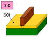
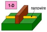
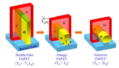
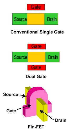
9 Reduction of FET Dimensionality Low Dimensionality? Best electrostatics Smallest structure for carrier transport (1-D) Energy efficiency design Quantum confinement/carrier mobility Device-interconnect co-design Top-Down technology limits, costs Multi-gate FET FinFET (2003) FinFET (2006) Fin-memory (2006) FinFET SRAM (2005)


10 esensor Web Robot Colony Nano-electronic components Europa Sub RLV Bio-mimetic molecular computing Bio-systems electronics interface SNW/CNT devices Ultra high density storage Computing Capacity Nanotechnology is the enabling technology driving numerous applications. The core concept of bottom-up is to employ cheap chemistry to promote selfassembly of functional components. New materials and technologies are emerging for energy-efficient information processing devices.


11 Hierarchical Assembly Nano-systems Self-assembly Nano-components Inorganic Crystalline Nanostructures tube cube Crystal growth belt saw Reaction chemistry disk tetrapod Organic/Bio Molecular Nanostructures wire monolayer comb windmill Material synthesis Single molecule Surface chemistry wire supramolecules Organic synthesis Molecular engineering
 Method Laser ablation PVD CVD (thermal CVD, LPCVD, PECVD, MOCVD) Vapor-Solid (VS) Method Oxide-Assisted Growth")
12 Solution-Phase Synthesis Solution-Liquid-Solid (SLS) Method Solvothermal Chemical Synthesis Template-Based Synthesis Gas-Phase Synthesis Vapor-Liquid-Solid (VLS) Method Laser ablation PVD CVD (thermal CVD, LPCVD, PECVD, MOCVD) Vapor-Solid (VS) Method Oxide-Assisted Growth (OAG)

13 Thermal CVD Thermal PVD
14
: solar cell, spintronics, sensors Chalcogenides (GeTe, GeSb, Ge2Sb2Te5, Sb2Te3): phase-change memory Ferroelectric metal oxide (BaTiO3): data")
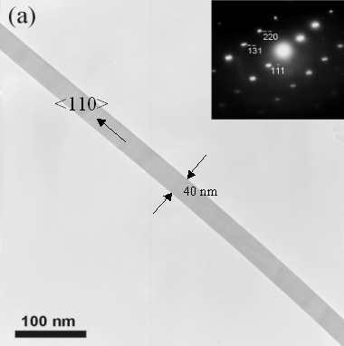
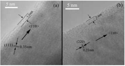
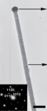
15 10+ types of low-dimensional nanostructures within five major categories: IV group elemental semiconductors (Si, Ge): computing/data storage III-V group compound semiconductor (InSb): computing, spintronics, optoelectronics, TE Metal oxide (ZnO, TiO2): solar cell, spintronics, sensors Chalcogenides (GeTe, GeSb, Ge2Sb2Te5, Sb2Te3): phase-change memory Ferroelectric metal oxide (BaTiO3): data storage Material characterization Physical morphology (SEM, TEM), chemical composition (EDS, XPS), crystal structure (XRD, EDP), thermal property (in-situ heating & TEM imaging)
 III-V Group")
 nanoparticles or colloids as")


16 IV Group (Ge) Metal Oxide (ZnO) Growth Experiments: IV Group (Si) III-V Group (InSb) Selected CVD/PVD processes Metal (Au, In, Sb) nanoparticles or colloids as growth catalyst Vapor-liquid-solid growth Growth on various substrates (Si, SiO2, quartz, sapphire, ) Targeted Applications: Transistors Nonvolatile memories Sensors LEDs, lasers

17 Gas Flow Rate
")


")
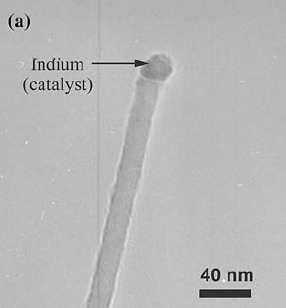
18 Indium (In) catalyst Ge-NW Catalyst Selection Ge-NW Antimony (Sb) catalyst Growth Orientations


19 TEM HR-TEM SAED EDS Elemental Mapping of GeSb Nanowire GeSb TEM Image Ge Mapping Sb Mapping


20 STM image of Ge nanowire di/dv STM tunneling current to measure Ge nanowire band-gap
21 Energy-efficient, scalable, high-performance transistor Nanoscale storage media to improve performance/density/ energy-efficiency High-efficiency solar cells & thermoelectrics Lower detection threshold (2-4 orders) at molecular or atomic level Component and assembly technology for future electronics featuring transparency, disposability, and flexibility


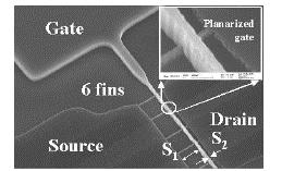
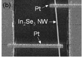
22 NiGe source Ge nanowire NiGe drain 4
23

24 Si-Based Memories Nano-Engineered Storage Devices Phased-Change Disruptive Storage Devices Molecular Floating-Gate MRAM Nanocrystal Carbon Nanotube Polymer Probe-Based Fin-Based Memory Nanowire


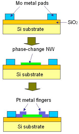
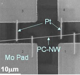
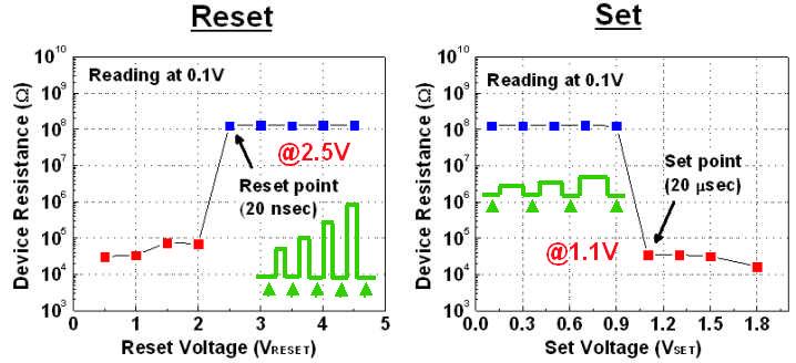
25 RESET SET RESET SET Pore and Lance Cell Structure -Trench Cell Structure Line Cell Structure
 Reduced thermal conductivity (1~2 orders mag.")
26 2-D Thin film 1-D Nanowire 0-D Nanodot Self-Assembly Growth Nano-Scale Physics Small size, highly scalable material system Large aspect ratio, etch-free process (one-step CVD) Perfect surface morphology Reduced melting point (30~50%) Reduced thermal conductivity (1~2 orders mag.) Projected Memory Features Ultra-low reset current (< 10 A/cell) Extremely low-cost manufacturing Break lithography limit w/ self-assembly


27 InSb Ge2 Sb2Te5 SbTe GeTe In2Se3
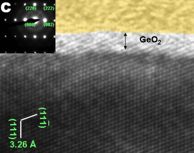
 electron diffraction pattern disappears, and (2)")

28 Tm of bulk PCM Tm of PCM nanowires Melting temperature of phasechange nanowire is identified as the point at which: (1) electron diffraction pattern disappears, and (2) nanowire starts to evaporate. This property is nanowire diameterdependent: more significant reduction at smaller diameters GeTe In2Se3 Bulk Tm 725 C 890 C Nanowire Tm 390 C 680 C % Reduction 46% 24%


29 Thermally induced nanowire encoding with scanning focused e-beam.
30 2 3
31 2/27/2008
32 Emerging Nano-Chip Architecture Inorganic Nanomaterial Synthesis Novel Device Technology Bio/Molecular Self-Assembly Nano-Research Program Modeling Simulation Nanostructure Characterization Nanofabrication Major emphasis will be on nano- and bio-materials self-assembly, physics, modeling, nanofabrication, and emerging device applications in (1) Nanoelectronics (2) Bioelectronics, and (3) Energy conversion devices Funding Resources: NSF, DOD, DOE, NASA, SRC Close Industry collaboration


33 Nano-Device Physics High-Performance Nanoelectronics - - Material Growth & Assembly Carrier transport property Quantum effects Strain-induced effects Thermal property/interface Field-effect transistors CMOS/logic units Quantum-wire devices Thin-Film Nanodevice Technology - Transparent devices Disposable chips - Low-Dimensional Electronics Controlled growth Large-scale assembly Composite structures Biological System Electronics Interface - Molecular interface/hybrid devices Biomimetic devices and circuits


34 Self-assembly: synthesis of structurally complex blocks Guided assembly: use physical or molecular templates Large-scale Assembly Heterogeneous Assembly Basic Assembly Assembly-Driven Fabrication Functional Devices Composite Elements Single NanoStructures s-nws m-nws CNTs CNFs NPs Junctions Hetero-structures Interconnects 3-D structures Core-shell Functional Units/Blocks Transistors Switches Storage cells Sensing cells Conversion cells Research Phase/Time Scale Large scale array Stacking Multi-substrates Templates Circuits Functional blocks Sub-systems
 Active Crossbar Array Contains")


35 Passive Crossbar Array Served as interconnect (local & global) Active Crossbar Array Contains element of programmable logic, data storage, and sensing Fundamental Issues: How to suppress leakage and power? Innovative selecting device technology? WLj-1 WLj WLj+1 WLj+2 BLi-1 BLi BL SL i+1 BLi+2
36 Bio-reaction Use of biomolecules as the building elements in a group of functional devices for information detection and processing Communication between biomolecules to nano electronics, e.g., Electron transfer Charge storage Biomoleculessemiconductor interface Neuron-nanowire interface Electronic Detection

37 Research will be focused on utilizing biomolecules as functional building elements to design energy-efficient, bio-mimetic devices and circuits with functionality that currently silicon-based chip technology is conducting.
 Tunable")


 Bio-fuel cell use")
38 Why Nanomaterials? High-conversion efficiency (surface-intensive structures) Tunable band-gap (wide spectrum light harvesting) Low-cost (thin film based) Possible materials: s-nws, m-nws, CNTs 3rd generation 4th generation Biology-Based Nano-Based 2nd generation Thin-Film-Based 1st generation Silicon-Based Why Biomaterials? Bio-enabled solar cells utilizing biomolecules to convert solar energy into chemical energy (similar to photosynthesis) Bio-fuel cell use body fluids as a fuel for the electrical powering of implantable devices Research Phase/Time Scale
There's Plenty of Room at the Bottom
 There's Plenty of Room at the Bottom 12/29/1959 Feynman asked why not put the entire Encyclopedia Britannica (24 volumes) on a pin head (requires atomic scale recording). He proposed to use electron microscope
RAJASTHAN TECHNICAL UNIVERSITY, KOTA
 RAJASTHAN TECHNICAL UNIVERSITY, KOTA (Electronics & Communication) Submitted By: LAKSHIKA SOMANI E&C II yr, IV sem. Session: 2007-08 Department of Electronics & Communication Geetanjali Institute of Technical
Nanostructure. Materials Growth Characterization Fabrication. More see Waser, chapter 2
 Nanostructure Materials Growth Characterization Fabrication More see Waser, chapter 2 Materials growth - deposition deposition gas solid Physical Vapor Deposition Chemical Vapor Deposition Physical Vapor
A final review session will be offered on Thursday, May 10 from 10AM to 12noon in 521 Cory (the Hogan Room).
.") A final review session will be offered on Thursday, May 10 from 10AM to 12noon in 521 Cory (the Hogan Room). The Final Exam will take place from 12:30PM to 3:30PM on Saturday May 12 in 60 Evans.» All of
A final review session will be offered on Thursday, May 10 from 10AM to 12noon in 521 Cory (the Hogan Room). The Final Exam will take place from 12:30PM to 3:30PM on Saturday May 12 in 60 Evans.» All of
Seminars in Nanosystems - I
 Seminars in Nanosystems - I Winter Semester 2011/2012 Dr. Emanuela Margapoti Emanuela.Margapoti@wsi.tum.de Dr. Gregor Koblmüller Gregor.Koblmueller@wsi.tum.de Seminar Room at ZNN 1 floor Topics of the
1. Introduction : 1.2 New properties:
 Nanodevices In Electronics Rakesh Kasaraneni(PID : 4672248) Department of Electrical Engineering EEL 5425 Introduction to Nanotechnology Florida International University Abstract : This paper describes
Nanoparticle Devices. S. A. Campbell, ECE C. B. Carter, CEMS H. Jacobs, ECE J. Kakalios, Phys. U. Kortshagen, ME. Institute of Technology
 Nanoparticle Devices S. A. Campbell, ECE C. B. Carter, CEMS H. Jacobs, ECE J. Kakalios, Phys. U. Kortshagen, ME Applications of nanoparticles Flash Memory Tiwari et al., Appl. Phys. Lett. 68, 1377, 1996.
master thesis STM studies of molecules for molecular electronics
 STM studies of molecules for molecular electronics Experimental study of single organic molecules by Scanning Tunneling Microscope (STM) and spectroscopy at low temperature Experimental STM images of Aza-BODIPY
Carbon Nanomaterials: Nanotubes and Nanobuds and Graphene towards new products 2030
 Carbon Nanomaterials: Nanotubes and Nanobuds and Graphene towards new products 2030 Prof. Dr. Esko I. Kauppinen Helsinki University of Technology (TKK) Espoo, Finland Forecast Seminar February 13, 2009
Nanotechnology. Yung Liou P601 Institute of Physics Academia Sinica
 Nanotechnology Yung Liou P601 yung@phys.sinica.edu.tw Institute of Physics Academia Sinica 1 1st week Definition of Nanotechnology The Interagency Subcommittee on Nanoscale Science, Engineering and Technology
Chapter 10. Nanometrology. Oxford University Press All rights reserved.
 Chapter 10 Nanometrology Oxford University Press 2013. All rights reserved. 1 Introduction Nanometrology is the science of measurement at the nanoscale level. Figure illustrates where nanoscale stands
Carbon Nanotube Thin-Films & Nanoparticle Assembly
 Nanodevices using Nanomaterials : Carbon Nanotube Thin-Films & Nanoparticle Assembly Seung-Beck Lee Division of Electronics and Computer Engineering & Department of Nanotechnology, Hanyang University,
There s plenty of room at the bottom! - R.P. Feynman, Nanostructure: a piece of material with at least one dimension less than 100 nm in extent.
 Nanostructures and Nanotechnology There s plenty of room at the bottom! - R.P. Feynman, 1959 Materials behave differently when structured at the nm scale than they do in bulk. Technologies now exist that
Special Topics in Semiconductor Nanotechnology ECE 598XL
 Special Topics in Semiconductor Nanotechnology ECE 598XL Fall 2009 ECE 598XL Syllabus Overview: size matters Formation Process Characterization SOA device applications and potentials Homework or quizzes
Chapter 12. Nanometrology. Oxford University Press All rights reserved.
 Chapter 12 Nanometrology Introduction Nanometrology is the science of measurement at the nanoscale level. Figure illustrates where nanoscale stands in relation to a meter and sub divisions of meter. Nanometrology
EE410 vs. Advanced CMOS Structures
 EE410 vs. Advanced CMOS Structures Prof. Krishna S Department of Electrical Engineering S 1 EE410 CMOS Structure P + poly-si N + poly-si Al/Si alloy LPCVD PSG P + P + N + N + PMOS N-substrate NMOS P-well
Current and Emergent Developments
 Self Assembly and Biologically Inspired Processes in Applied Nanotechnology: Current and Emergent Developments Charles Ostman VP, Electronics & Photonics Forum chair NanoSig Senior Consultant Silicon Valley
1. Nanotechnology & nanomaterials -- Functional nanomaterials enabled by nanotechnologies.
 Novel Nano-Engineered Semiconductors for Possible Photon Sources and Detectors NAI-CHANG YEH Department of Physics, California Institute of Technology 1. Nanotechnology & nanomaterials -- Functional nanomaterials
Chapter 1 Introduction
 Chapter 1 Introduction A nanometer (nm) is one billionth (10-9 ) of a meter. Nanoscience can be defined as the science of objects and phenomena occurring at the scale of 1 to 100 nm. The range of 1 100
In the name of Allah
 In the name of Allah Nano chemistry- 4 th stage Lecture No. 1 History of nanotechnology 16-10-2016 Assistance prof. Dr. Luma Majeed Ahmed lumamajeed2013@gmail.com, luma.ahmed@uokerbala.edu.iq Nano chemistry-4
Nanotechnology Fabrication Methods.
 Nanotechnology Fabrication Methods. 10 / 05 / 2016 1 Summary: 1.Introduction to Nanotechnology:...3 2.Nanotechnology Fabrication Methods:...5 2.1.Top-down Methods:...7 2.2.Bottom-up Methods:...16 3.Conclusions:...19
From nanophysics research labs to cell phones. Dr. András Halbritter Department of Physics associate professor
 From nanophysics research labs to cell phones Dr. András Halbritter Department of Physics associate professor Curriculum Vitae Birth: 1976. High-school graduation: 1994. Master degree: 1999. PhD: 2003.
Nanotechnology Nanofabrication of Functional Materials. Marin Alexe Max Planck Institute of Microstructure Physics, Halle - Germany
 Nanotechnology Nanofabrication of Functional Materials Marin Alexe Max Planck Institute of Microstructure Physics, Halle - Germany Contents Part I History and background to nanotechnology Nanoworld Nanoelectronics
Materials. Definitions of nanotechnology. The term nanotechnology was invented by Professor Norio Taniguchi at the University of Tokyo in 1971.
 Materials Definitions of nanotechnology The term nanotechnology was invented by Professor Norio Taniguchi at the University of Tokyo in 1971. The original definition, translated into English Nano-technology'
Molecular Electronics For Fun and Profit(?)
") Molecular Electronics For Fun and Profit(?) Prof. Geoffrey Hutchison Department of Chemistry University of Pittsburgh geoffh@pitt.edu July 22, 2009 http://hutchison.chem.pitt.edu Moore s Law: Transistor
Molecular Electronics For Fun and Profit(?) Prof. Geoffrey Hutchison Department of Chemistry University of Pittsburgh geoffh@pitt.edu July 22, 2009 http://hutchison.chem.pitt.edu Moore s Law: Transistor
Low Power Phase Change Memory via Block Copolymer Self-assembly Technology
 Low Power Phase Change Memory via Block Copolymer Self-assembly Technology Beom Ho Mun 1, Woon Ik Park 1, You Yin 2, Byoung Kuk You 1, Jae Jin Yun 1, Kung Ho Kim 1, Yeon Sik Jung 1*, and Keon Jae Lee 1*
29: Nanotechnology. What is Nanotechnology? Properties Control and Understanding. Nanomaterials
 29: Nanotechnology What is Nanotechnology? Properties Control and Understanding Nanomaterials Making nanomaterials Seeing at the nanoscale Quantum Dots Carbon Nanotubes Biology at the Nanoscale Some Applications
CSCI 2570 Introduction to Nanocomputing
 CSCI 2570 Introduction to Nanocomputing The Emergence of Nanotechnology John E Savage Purpose of the Course The end of Moore s Law is in sight. Researchers are now exploring replacements for standard methods
Wafer-scale fabrication of graphene
 Wafer-scale fabrication of graphene Sten Vollebregt, MSc Delft University of Technology, Delft Institute of Mircosystems and Nanotechnology Delft University of Technology Challenge the future Delft University
Graphene Fundamentals and Emergent Applications
 Graphene Fundamentals and Emergent Applications Jamie H. Warner Department of Materials University of Oxford Oxford, UK Franziska Schaffel Department of Materials University of Oxford Oxford, UK Alicja
Trends in Nanotechnology: Self-Assembly and Defect Tolerance
 Trends in Nanotechnology: Self-Assembly and Defect Tolerance (Invited paper submitted to MSTNEWS 3 January 2001) T. I. Kamins and R. Stanley Williams Quantum Science Research, Hewlett-Packard Laboratories,
Administrative Stuff
 EE141- Spring 2004 Digital Integrated Circuits Lecture 30 PERSPECTIVES 1 Administrative Stuff Homework 10 posted just for practice. No need to turn in (hw 9 due today). Normal office hours next week. HKN
Gold Nanoparticles Floating Gate MISFET for Non-Volatile Memory Applications
 Gold Nanoparticles Floating Gate MISFET for Non-Volatile Memory Applications D. Tsoukalas, S. Kolliopoulou, P. Dimitrakis, P. Normand Institute of Microelectronics, NCSR Demokritos, Athens, Greece S. Paul,
Scaling up Chemical Vapor Deposition Graphene to 300 mm Si substrates
 Scaling up Chemical Vapor Deposition Graphene to 300 mm Si substrates Co- Authors Aixtron Alex Jouvray Simon Buttress Gavin Dodge Ken Teo The work shown here has received partial funding from the European
3/10/2013. Lecture #1. How small is Nano? (A movie) What is Nanotechnology? What is Nanoelectronics? What are Emerging Devices?
 What is Nanotechnology? What is Nanoelectronics? What are Emerging Devices?") EECS 498/598: Nanocircuits and Nanoarchitectures Lecture 1: Introduction to Nanotelectronic Devices (Sept. 5) Lectures 2: ITRS Nanoelectronics Road Map (Sept 7) Lecture 3: Nanodevices; Guest Lecture by
EECS 498/598: Nanocircuits and Nanoarchitectures Lecture 1: Introduction to Nanotelectronic Devices (Sept. 5) Lectures 2: ITRS Nanoelectronics Road Map (Sept 7) Lecture 3: Nanodevices; Guest Lecture by
Device 3D. 3D Device Simulator. Nano Scale Devices. Fin FET
 Device 3D 3D Device Simulator Device 3D is a physics based 3D device simulator for any device type and includes material properties for the commonly used semiconductor materials in use today. The physical
ME 4875/MTE C16. Introduction to Nanomaterials and Nanotechnology. Lecture 2 - Applications of Nanomaterials + Projects
 ME 4875/MTE 575 - C16 Introduction to Nanomaterials and Nanotechnology Lecture 2 - Applications of Nanomaterials + Projects 1 Project Teams of 4 students each Literature review of one application of nanotechnology
SELF-ASSEMBLY AND NANOTECHNOLOGY A Force Balance Approach
 SELF-ASSEMBLY AND NANOTECHNOLOGY A Force Balance Approach Yoon S. Lee Scientific Information Analyst Chemical Abstracts Service A Division of the American Chemical Society Columbus, Ohio WILEY A JOHN WILEY
12. Memories / Bipolar transistors
 Technische Universität Graz Institute of Solid State Physics 12. Memories / Bipolar transistors Jan. 9, 2019 Technische Universität Graz Institute of Solid State Physics Exams January 31 March 8 May 17
Physicists in the Semiconductor Industry
 Physicists in the Semiconductor Industry P.M. Mooney IBM Research Division, T.J. Watson Research Center Yorktown Heights, NY 10598 APS March Meeting March 24, 2004 Thomas J. Watson Research Center 1 Outline
Fabrication at the nanoscale for nanophotonics
 Fabrication at the nanoscale for nanophotonics Ilya Sychugov, KTH Materials Physics, Kista silicon nanocrystal by electron beam induced deposition lithography Outline of basic nanofabrication methods Devices
Goal: To use DNA self-assembly to overcome the challenges of optical and e-beam lithography in creating nanoscale circuits.
 Goal: To use DNA self-assembly to overcome the challenges of optical and e-beam lithography in creating nanoscale circuits. PI Paul Rothemund, computer scientist, Senior Research Associate (research faculty)
Cross Reference Art Collection Class 977 NANOTECHNOLOGY (April 19, 2005)
") Cross Reference Art Collection Class 977 NANOTECHNOLOGY (April 19, 2005) 7200E NANOSTRUCTURE 7240D. Integrated with dissimilar structures on a common substrate 7355C.. Having biological material component
Cross Reference Art Collection Class 977 NANOTECHNOLOGY (April 19, 2005) 7200E NANOSTRUCTURE 7240D. Integrated with dissimilar structures on a common substrate 7355C.. Having biological material component
NANOTECHNOLOGY FOR ELECTRONICS AND SENSORS APPLICATIONS
 NANOTECHNOLOGY FOR ELECTRONICS AND SENSORS APPLICATIONS SMALLER FASTER MORE SENSETIVE MORE EFFICIENT NANO CONNECT SCANDINAVIA www.nano-connect.org Chalmers University of Technology DTU Halmstad University
ETH Rüschlikon the people and their research
 ETH Zurich @ Rüschlikon the people and their research Prof. Dr. Dimos Poulikakos, Laboratory of Thermodynamics in Emerging Technologies and Coordinator of the Nanotechnology Center, ETH Zurich The Vision
What are Carbon Nanotubes? What are they good for? Why are we interested in them?
 Growth and Properties of Multiwalled Carbon Nanotubes What are Carbon Nanotubes? What are they good for? Why are we interested in them? - Interconnects of the future? - our vision Where do we stand - our
2D Materials for Gas Sensing
 2D Materials for Gas Sensing S. Guo, A. Rani, and M.E. Zaghloul Department of Electrical and Computer Engineering The George Washington University, Washington DC 20052 Outline Background Structures of
Nano-mechatronics. Presented by: György BudaváriSzabó (X0LY4M)
") Nano-mechatronics Presented by: György BudaváriSzabó (X0LY4M) Nano-mechatronics Nano-mechatronics is currently used in broader spectra, ranging from basic applications in robotics, actuators, sensors,
Nano-mechatronics Presented by: György BudaváriSzabó (X0LY4M) Nano-mechatronics Nano-mechatronics is currently used in broader spectra, ranging from basic applications in robotics, actuators, sensors,
The goal of this project is to enhance the power density and lowtemperature efficiency of solid oxide fuel cells (SOFC) manufactured by atomic layer
 manufactured by atomic layer") Stanford University Michael Shandalov1, Shriram Ramanathan2, Changhyun Ko2 and Paul McIntyre1 1Department of Materials Science and Engineering, Stanford University 2Division of Engineering and Applied
Stanford University Michael Shandalov1, Shriram Ramanathan2, Changhyun Ko2 and Paul McIntyre1 1Department of Materials Science and Engineering, Stanford University 2Division of Engineering and Applied
N ano scale l S il ii lco i n B ased N o nvo lat l i atl ie l M em ory r Chungwoo Kim, Ph.D.
 cw_kim@samsung.com Acknowledgements Collaboration Funding Outline Introduction Current research status Nano fabrication Process Nanoscale patterning SiN thin film Si Nanoparticle Nano devices Nanoscale
Nanostrukturphysik (Nanostructure Physics)
") Nanostrukturphysik (Nanostructure Physics) Prof. Yong Lei & Dr. Yang Xu Fachgebiet 3D-Nanostrukturierung, Institut für Physik Contact: yong.lei@tu-ilmenau.de; yang.xu@tu-ilmenau.de Office: Unterpoerlitzer
Nanostrukturphysik (Nanostructure Physics) Prof. Yong Lei & Dr. Yang Xu Fachgebiet 3D-Nanostrukturierung, Institut für Physik Contact: yong.lei@tu-ilmenau.de; yang.xu@tu-ilmenau.de Office: Unterpoerlitzer
ESH Benign Processes for he Integration of Quantum Dots (QDs)
") ESH Benign Processes for he Integration of Quantum Dots (QDs) PIs: Karen K. Gleason, Department of Chemical Engineering, MIT Graduate Students: Chia-Hua Lee: PhD Candidate, Department of Material Science
ESH Benign Processes for he Integration of Quantum Dots (QDs) PIs: Karen K. Gleason, Department of Chemical Engineering, MIT Graduate Students: Chia-Hua Lee: PhD Candidate, Department of Material Science
Overview. Carbon in all its forms. Background & Discovery Fabrication. Important properties. Summary & References. Overview of current research
 Graphene Prepared for Solid State Physics II Pr Dagotto Spring 2009 Laurene Tetard 03/23/09 Overview Carbon in all its forms Background & Discovery Fabrication Important properties Overview of current
DocumentToPDF trial version, to remove this mark, please register this software.
 PAPER PRESENTATION ON Carbon Nanotube - Based Nonvolatile Random Access Memory AUTHORS M SIVARAM PRASAD Sivaram.443@gmail.com B N V PAVAN KUMAR pavankumar.bnv@gmail.com 1 Carbon Nanotube- Based Nonvolatile
CHAPTER I. Introduction. 1.1 State of the art for non-volatile memory
 CHAPTER I Introduction 1.1 State of the art for non-volatile memory 1.1.1 Basics of non-volatile memory devices In the last twenty years, microelectronics has been strongly developed, concerning higher
Ultralow-Power Reconfigurable Computing with Complementary Nano-Electromechanical Carbon Nanotube Switches
 Ultralow-Power Reconfigurable Computing with Complementary Nano-Electromechanical Carbon Nanotube Switches Presenter: Tulika Mitra Swarup Bhunia, Massood Tabib-Azar, and Daniel Saab Electrical Eng. And
Physics and Material Science of Semiconductor Nanostructures
 Physics and Material Science of Semiconductor Nanostructures PHYS 570P Prof. Oana Malis Email: omalis@purdue.edu Course website: http://www.physics.purdue.edu/academic_programs/courses/phys570p/ 1 Course
Nanocarbon Technology for Development of Innovative Devices
 Nanocarbon Technology for Development of Innovative Devices Shintaro Sato Daiyu Kondo Shinichi Hirose Junichi Yamaguchi Graphene, a one-atom-thick honeycomb lattice made of carbon, and a carbon nanotube,
Stretching the Barriers An analysis of MOSFET Scaling. Presenters (in order) Zeinab Mousavi Stephanie Teich-McGoldrick Aseem Jain Jaspreet Wadhwa
 Zeinab Mousavi Stephanie Teich-McGoldrick Aseem Jain Jaspreet Wadhwa") Stretching the Barriers An analysis of MOSFET Scaling Presenters (in order) Zeinab Mousavi Stephanie Teich-McGoldrick Aseem Jain Jaspreet Wadhwa Why Small? Higher Current Lower Gate Capacitance Higher
Stretching the Barriers An analysis of MOSFET Scaling Presenters (in order) Zeinab Mousavi Stephanie Teich-McGoldrick Aseem Jain Jaspreet Wadhwa Why Small? Higher Current Lower Gate Capacitance Higher
CMOS Scaling. Two motivations to scale down. Faster transistors, both digital and analog. To pack more functionality per area. Lower the cost!
 Two motivations to scale down CMOS Scaling Faster transistors, both digital and analog To pack more functionality per area. Lower the cost! (which makes (some) physical sense) Scale all dimensions and
Contents. Preface to the first edition
 Contents List of authors Preface to the first edition Introduction x xi xiii 1 The nanotechnology revolution 1 1.1 From micro- to nanoelectronics 2 1.2 From the macroscopic to the nanoscopic world 4 1.3
Lecture 6: Individual nanoparticles, nanocrystals and quantum dots
 Lecture 6: Individual nanoparticles, nanocrystals and quantum dots Definition of nanoparticle: Size definition arbitrary More interesting: definition based on change in physical properties. Size smaller
MTJ-Based Nonvolatile Logic-in-Memory Architecture and Its Application
 2011 11th Non-Volatile Memory Technology Symposium @ Shanghai, China, Nov. 9, 20112 MTJ-Based Nonvolatile Logic-in-Memory Architecture and Its Application Takahiro Hanyu 1,3, S. Matsunaga 1, D. Suzuki
NANOTECHNOLOGY SUSTAINABILITY
 NANOTECHNOLOGY THE KEY TO SUSTAINABILITY Ankara, Oct. 4, 2010 THIS IS NOT MEANT TO BE A GREEN CRUSADE IT IS A REMINDER THAT SCIENCE PROVIDES WHAT MANKIND NEEDS BUT MANKIND HAS TO MAKE THE CHOICE WORKING
2D MBE Activities in Sheffield. I. Farrer, J. Heffernan Electronic and Electrical Engineering The University of Sheffield
 2D MBE Activities in Sheffield I. Farrer, J. Heffernan Electronic and Electrical Engineering The University of Sheffield Outline Motivation Van der Waals crystals The Transition Metal Di-Chalcogenides
Lecture 6. Alternative storage technologies. All optical recording. Racetrack memory. Topological kink solitons. Flash memory. Holographic memory
 Lecture 6 Alternative storage technologies All optical recording Racetrack memory Topological kink solitons Flash memory Holographic memory Millipede Ferroelectric memory All-optical recording It is possible
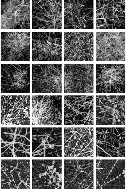
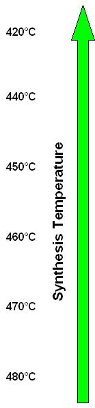
D DAVID PUBLISHING. Study the Synthesis Parameter of Tin Oxide Nanostructure. 1. Introduction. 2. Experiment
 Journal of Materials Science and Engineering B 5 (9-10) (2015) 353-360 doi: 10.17265/2161-6221/2015.9-10.003 D DAVID PUBLISHING Study the Synthesis Parameter of Tin Oxide Nanostructure Gyanendra Prakash
Introduction to Nanotechnology Chapter 5 Carbon Nanostructures Lecture 1
 Introduction to Nanotechnology Chapter 5 Carbon Nanostructures Lecture 1 ChiiDong Chen Institute of Physics, Academia Sinica chiidong@phys.sinica.edu.tw 02 27896766 Carbon contains 6 electrons: (1s) 2,
Physics and Material Science of Semiconductor Nanostructures
 Physics and Material Science of Semiconductor Nanostructures PHYS 570P Prof. Oana Malis Email: omalis@purdue.edu Course website: http://www.physics.purdue.edu/academic_programs/courses/phys570p/ Lecture
NANOELECTRONICS beyond CMOS
 NANOELECTRONICS beyond CMOS David Pulfrey 1 NNI definition of Nanotechnology 1-10 nm is better But Intel prefer... 2 Bourianoff04 1 3 Bourianoff04 4 Moravec04 2 Increasing the Integration Level functional
State of São Paulo. Brasil. Localization. Santo André
 Brasil State of São Paulo Localization Santo André The Group www.crespilho.com Frank N. Crespilho Pablo R. S. Abdias Group Leader Synthesis of nanostructured materials using polyelectrolytes Andressa R.
EV Group. Engineered Substrates for future compound semiconductor devices
 EV Group Engineered Substrates for future compound semiconductor devices Engineered Substrates HB-LED: Engineered growth substrates GaN / GaP layer transfer Mobility enhancement solutions: III-Vs to silicon
Film Deposition Part 1
 1 Film Deposition Part 1 Chapter 11 : Semiconductor Manufacturing Technology by M. Quirk & J. Serda Spring Semester 2013 Saroj Kumar Patra Semidonductor Manufacturing Technology, Norwegian University of
Center for Integrated Nanotechnologies (CINT) Bob Hwang Co-Director, Sandia National Laboratories
 Bob Hwang Co-Director, Sandia National Laboratories") Center for Integrated Nanotechnologies (CINT) Bob Hwang Co-Director, Sandia National Laboratories Department of Energy Nanoscience Centers Molecular Foundry Center for Nanoscale Materials Center for Functional
Center for Integrated Nanotechnologies (CINT) Bob Hwang Co-Director, Sandia National Laboratories Department of Energy Nanoscience Centers Molecular Foundry Center for Nanoscale Materials Center for Functional
How a single defect can affect silicon nano-devices. Ted Thorbeck
 How a single defect can affect silicon nano-devices Ted Thorbeck tedt@nist.gov The Big Idea As MOS-FETs continue to shrink, single atomic scale defects are beginning to affect device performance Gate Source
Challenges for Materials to Support Emerging Research Devices
 Challenges for Materials to Support Emerging Research Devices C. Michael Garner*, James Hutchby +, George Bourianoff*, and Victor Zhirnov + *Intel Corporation Santa Clara, CA + Semiconductor Research Corporation
Institute for Electron Microscopy and Nanoanalysis Graz Centre for Electron Microscopy
 Institute for Electron Microscopy and Nanoanalysis Graz Centre for Electron Microscopy Micromechanics Ass.Prof. Priv.-Doz. DI Dr. Harald Plank a,b a Institute of Electron Microscopy and Nanoanalysis, Graz
Emerging Research Materials and Processes
 Recipient of the 2005 National Medal of Technology Emerging Research Materials and Processes Center For Hierarchical Manufacturing - National Nanomanufacturing Network: Nanomanufacturing Systems Workshop
Nanoparticles, nanorods, nanowires
 Nanoparticles, nanorods, nanowires Nanoparticles, nanocrystals, nanospheres, quantum dots, etc. Drugs, proteins, etc. Nanorods, nanowires. Optical and electronic properties. Organization using biomolecules.
Thin Film Transistors (TFT)
") Thin Film Transistors (TFT) a-si TFT - α-si:h (Hydrogenated amorphous Si) deposited with a PECVD system (low temp. process) replaces the single crystal Si substrate. - Inverted staggered structure with
Thin Film Transistors (TFT) a-si TFT - α-si:h (Hydrogenated amorphous Si) deposited with a PECVD system (low temp. process) replaces the single crystal Si substrate. - Inverted staggered structure with
Call for Papers. 3 Steps to Contribute a Presentation. Submit. Submission Deadline: June 26 (Tue.), 2018 (17:00, JST)
, 2018 (17:00, JST)") Call for Papers 3 Steps to Contribute a Presentation Join JSAP Submit Register Regular Membership Admission Fee: 10,000 JPY Annual Due*: 10,000 JPY *Annual due will be waived for the first year. Graduate
Call for Papers 3 Steps to Contribute a Presentation Join JSAP Submit Register Regular Membership Admission Fee: 10,000 JPY Annual Due*: 10,000 JPY *Annual due will be waived for the first year. Graduate
Recap (so far) Low-Dimensional & Boundary Effects
 Low-Dimensional & Boundary Effects") Recap (so far) Ohm s & Fourier s Laws Mobility & Thermal Conductivity Heat Capacity Wiedemann-Franz Relationship Size Effects and Breakdown of Classical Laws 1 Low-Dimensional & Boundary Effects Energy
Recap (so far) Ohm s & Fourier s Laws Mobility & Thermal Conductivity Heat Capacity Wiedemann-Franz Relationship Size Effects and Breakdown of Classical Laws 1 Low-Dimensional & Boundary Effects Energy
Monolayer Semiconductors
 Monolayer Semiconductors Gilbert Arias California State University San Bernardino University of Washington INT REU, 2013 Advisor: Xiaodong Xu (Dated: August 24, 2013) Abstract Silicon may be unable to
Photoresponsive Nanoscale Columnar Transistors
 Photoresponsive Nanoscale Columnar Transistors Xuefeng Guo, Shengxiong Xiao, Matthew Myers, Qian Miao, Michael L. Steigerwald, and Colin Nuckolls. Center for Nanochemistry, Beijing National Laboratory
Nanostructures. Lecture 13 OUTLINE
 Nanostructures MTX9100 Nanomaterials Lecture 13 OUTLINE -What is quantum confinement? - How can zero-dimensional materials be used? -What are one dimensional structures? -Why does graphene attract so much
Nanofabrication/Nano-Characterization Calixarene and CNT Control Technology
 Nanofabrication/Nano-Characterization Calixarene and CNT Control Technology ISHIDA Masahiko, FUJITA Junichi, NARIHIRO Mitsuru, ICHIHASHI Toshinari, NIHEY Fumiyuki, OCHIAI Yukinori Abstract The world of
Nanostructures. Nanomaterials Synthesis, Properties, and Applications
 Nanostructures and Nanomaterials Synthesis, Properties, and Applications 2nd Edition World Scientific Series in Nanoscience and Nanotechnology Series Editor: Mark Reed (Yale University) Vol. 1 Vol. 2 Molecular
Jay A. Switzer Summary of Research
 Jay A. Switzer Summary of Research I have dedicated most of my career to research on the electrodeposition of nanostructured metal oxide ceramics. Although the electroplating of metal films is a mature
Lecture 0: Introduction
 Lecture 0: Introduction Introduction q Integrated circuits: many transistors on one chip q Very Large Scale Integration (VLSI): bucketloads! q Complementary Metal Oxide Semiconductor Fast, cheap, low power
EN2912C: Future Directions in Computing Lecture 08: Overview of Near-Term Emerging Computing Technologies
 EN2912C: Future Directions in Computing Lecture 08: Overview of Near-Term Emerging Computing Technologies Prof. Sherief Reda Division of Engineering Brown University Fall 2008 1 Near-term emerging computing
Forming Gradient Multilayer (GML) Nano Films for Photovoltaic and Energy Storage Applications
 Nano Films for Photovoltaic and Energy Storage Applications") Forming Gradient Multilayer (GML) Nano Films for Photovoltaic and Energy Storage Applications ABSTRACT Boris Gilman and Igor Altman Coolsol R&C, Mountain View CA For successful implementation of the nanomaterial-based
Forming Gradient Multilayer (GML) Nano Films for Photovoltaic and Energy Storage Applications ABSTRACT Boris Gilman and Igor Altman Coolsol R&C, Mountain View CA For successful implementation of the nanomaterial-based
Nanomaterials and their Optical Applications
 Nanomaterials and their Optical Applications Winter Semester 2013 Lecture 02 rachel.grange@uni-jena.de http://www.iap.uni-jena.de/multiphoton Lecture 2: outline 2 Introduction to Nanophotonics Theoretical
Nanotechnology? Source: National Science Foundation (NSF), USA
, USA") 2 2 Nanotechnology? Ability to work at the atomic, molecular and even sub-molecular levels in order to create and use material structures, devices and systems with new properties and functions Source:
2 2 Nanotechnology? Ability to work at the atomic, molecular and even sub-molecular levels in order to create and use material structures, devices and systems with new properties and functions Source:
what happens if we make materials smaller?
 what happens if we make materials smaller? IAP VI/10 ummer chool 2007 Couvin Prof. ns outline Introduction making materials smaller? ynthesis how do you make nanomaterials? Properties why would you make
Carbon Nanotubes in Interconnect Applications
 Carbon Nanotubes in Interconnect Applications Page 1 What are Carbon Nanotubes? What are they good for? Why are we interested in them? - Interconnects of the future? Comparison of electrical properties
Oxide Films & Nanostructures on Silicon for Thermal Energy Harvesting in Microelectronic Devices
 Oxide Films & Nanostructures on Silicon for Thermal Energy Harvesting in Microelectronic Devices R. Bachelet R. Moalla, A. Carretero-Genevrier, L. Mazet, L. Louahadj, J. Penuelas, B. Vilquin, C. Dubourdieu,
Overview of Nanotechnology Applications and Relevant Intellectual Property NANO POWER PATENTS
 Overview of Nanotechnology Applications and Relevant Intellectual Property NANO POWER PATENTS Jeffrey H. Rosedale, Ph.D., J.D. Registered Patent Attorney Partner, Woodcock Washburn, LLP ~ 9000 Issued U.S.
Carbon Nanomaterials
 Carbon Nanomaterials STM Image 7 nm AFM Image Fullerenes C 60 was established by mass spectrographic analysis by Kroto and Smalley in 1985 C 60 is called a buckminsterfullerene or buckyball due to resemblance
NANO TECHNOLOGY IN POLYMER SOLAR CELLS. Mayur Padharia, Hardik Panchal, Keval Shah, *Neha Patni, Shibu.G.Pillai
 NANO TECHNOLOGY IN POLYMER SOLAR CELLS Mayur Padharia, Hardik Panchal, Keval Shah, *Neha Patni, Shibu.G.Pillai Department of Chemical Engineering, Institute of Technology, Nirma University, S. G. Highway,
Introduction to semiconductor nanostructures. Peter Kratzer Modern Concepts in Theoretical Physics: Part II Lecture Notes
 Introduction to semiconductor nanostructures Peter Kratzer Modern Concepts in Theoretical Physics: Part II Lecture Notes What is a semiconductor? The Fermi level (chemical potential of the electrons) falls