Organic Device Simulation Using Silvaco Software. Silvaco Taiwan September 2005
|
|
|
- Arron Daniel
- 5 years ago
- Views:
Transcription

1 Organic Device Simulation Using Silvaco Software Silvaco Taiwan September 2005
2 Organic Devices Simulation: Contents Introduction Silvaco TCAD Simulator Theory Models OTFT Simulation v.s Measurement OLED Simulation v.s Measurement Bilayer TPD/Alq3 OLED Example Transient Simulation of OLED Pixel Summary
3 Organic Devices Simulation: Silvaco s TCAD Software ATHENA - 2D Process Simulator ATLAS Device Simulator SPisces Silicon material Drift-Diffusion Simulator Blaze Hetero-interfaces (Compound Semiconductor) Materials Simulator TFT a-si/poly-si TFT Device Simulator OTFT Organic TFT Simulator OLED Organic Light Emitting Diode Simulator
4 Organic Devices Simulation: Transport Mechanisms Metal & Semiconductors: charge transport is limited by scattering of the carriers, mainly due to thermally induced phonons and lattice deformations. Transport is limited by phonon scattering. Charge mobility decreases with temperature Organic materials: transport occurs by phonon assisted hopping of charges between localized states. Charge mobility increases with temperature General mobility model of organic material : Poole-Frenkel field-dependent mobility
5 Organic Devices Simulation: Organic Transport TheoryFor Simulation Charge Injection (metal contact) Ohmic (Dirichlet boundary condition) Schottky contact (injection limited current) : thermionic emission model - tunneling interface barrier lowering Transport model(bulk) Band-like transport model (organic molecular crystals: pentacene, tetracene) at low T. Space-Charge-Limited Current(SCLC): Poisson + Current continuity equations Hopping transport in disordered organic semiconductor Density of States Poole-Frenkel Mobility
6 Organic Devices Simulation: Classical Theory Of Charge Transport Drift Diffusion Model Poisson Equation Current Continuity Equations Drift Diffusion Equations
7 Organic Devices Simulation: Density Of State & Trapped Charge Organic Defects Density Of States (DOS) Trapped Charge
8 Organic Devices Simulation: Organic Defects Probability of Occupation Steady State: Recombination/Generation (SRH)
9 Organic Devices Simulation: Poole-Frenkel Mobility Models
10 Organic Devices Simulation: Langevin Recombination Rate & Exciton Rate Equations Langevin Radiative Rate Singlet Exciton
11 Organic Devices Simulation: Langevin Recombination Rate & Exciton Rate Equations (con t) Triplet Exciton where
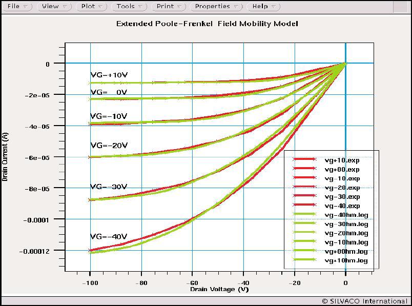
12 ATLAS Organic Device Simulation: Mobility Simulation Time-of-flight(TOF) method SCLC method Field Effect Transistor(FET) method


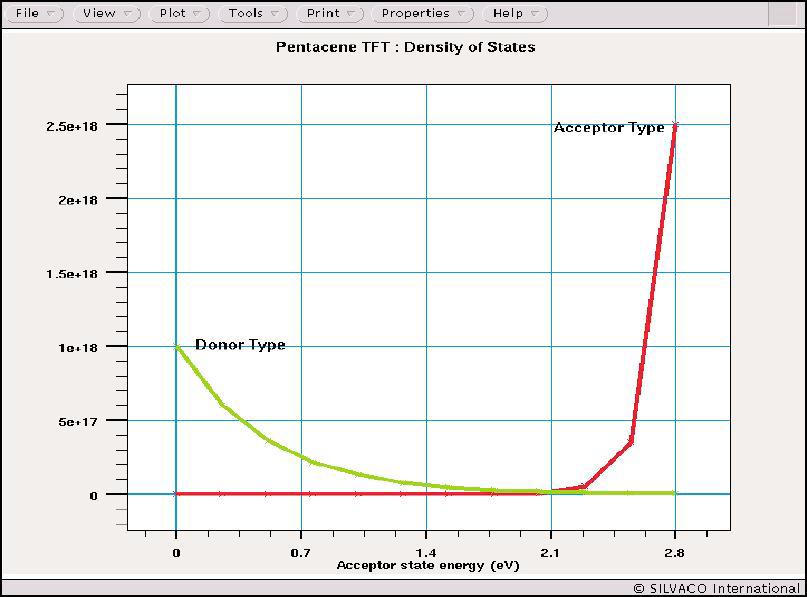
13 ATLAS Organic Device Simulation Measurement vs. Simulation p Density of States


14 ATLAS Organic TFT Device Simulation Transfer curve: linear & sqrt(ids)
,1 Feb 1994, p.")
15 ATLAS Organic LED Device Simulation: OLED Example Metal/Organic Interface injection I.D. Parker J.Appl. Phys. 75(3),1 Feb 1994, p.1656


16 ATLAS Organic LED Device Simulation Injection - Calcium Ca(2.9eV) is better than other cathode metal. Simulated Measured I.D. Parker J.Appl. Phys. 75(3),1 Feb 1994, p.1656
17 ATLAS Organic LED Device Simulation: High- Efficient Amorphous OLED Fraction of injected charge that form excitons

18 ATLAS Organic LED Device Simulation: Bilayer TPD/ Alq3 OLED Example: Singlet Exciton Density Profile Exciton Profile

19 ATLAS Organic LED Devices Simulation: Bilayer TPD/Alq3 OLED Example: IL & Internal Efficiency IL curve Internal Efficiency


20 ATLAS Organic LED Device Simulation: Bilayer TPD/Alq3 OLED Example: Optical Output Coupling n=1.5 n=1.9 n=1.8
21 Organic Device Simulation Transient Simulation of OLED Pixel
22 Organic Devices Simulation: Basic OLED Equivalent Circuit A p-type poly-si TFT AM-OLED pixel is shown The cathode and anode electrodes of the OLED form an intrinsic capacitance C and the resulting equivalent circuit is shown When it is connected to a poly- Si TFT with an on resistance R ON, it forms a circuit with its speed limited by the RC time constant

23 Organic Devices Simulation: Corresponding OLED Pixel Structure The device simulation structure of a p-type Poly-Si TFT AM-OLED pixel is shown here The structure is set up for device simulation and does not represent actual process steps More complicated OLED pixels can be simulated using Atlas MIXEDMODE
24 Organic Devices Simulation: OLED Pixel Simulation Curve 1: Transient current simulation results of the PPV OLED only (in blue) Curve 2: The combined poly-si TFT/OLED pixel (in black) note the effect of TFT on current level The rise/fall (ON/OFF) signal is coupled through the poly-si TFT and is converted as a current spike in the OLED as shown
25 Organic Devices Simulation: OLED Experiment The transient OLED current density response due to a 600ns square data voltage pulse of the experimental and simulation curves are characterized by: A sharp charging spike due to the capacitance of the device followed by a quasi-steady state At turn-off there is a sharp discharging spike followed by some decay * Pinner et al, J Appl Phys 86 (9) 5116

26 Organic Devices Simulation: Exciton Simulation A simulated transient result of the exciton density is shown The exciton density assumes a Langevin recombination process and takes into account singlet excitons, inclusive of diffusive and decay terms
27 Organic Devices Simulation: Experimental EL Curve* One can observe the fast initial EL rise followed by a slower rise, fast modulation in the turn-off, and a decaying exponential tail Assuming the exciton density is proportional to EL, note the similar shape of the previous exciton density simulation with the EL curve * Pinner et al, J Appl Phys 86 (9) 5116
28 Organic Devices Simulation: OLED Langevin Recombination Zone (2D plot)

29 Organic Devices Simulation: Langevin Recombination and Exciton Density Calculation of transient OLED Langevin recombination and exciton density based on 3 pulses

30 Organic Devices Simulation: PPV OLED Exciton Density (2D plot)
31 Organic Devices Simulation: Extraction of OLED Internal Efficiency IV-Curve Internal Efficiency Curve
32 Summary Organic Materials: Default Bandgap parameters. Others are defined by user-defined Density-Of-States(DOS) Transport: Drift-Diffusion/Poole-Frenkel mobility model Bimolecular Langevin Recombination Excition Rate Equation: singlet/triplet exciton profiles Radiative rate for luminescence or phosphorescence Reverse Ray-Tracing: external efficiency (refractive index step) Angular power plot/optical output coupling coefficient/near&far field distribution
Review Energy Bands Carrier Density & Mobility Carrier Transport Generation and Recombination
 Review Energy Bands Carrier Density & Mobility Carrier Transport Generation and Recombination The Metal-Semiconductor Junction: Review Energy band diagram of the metal and the semiconductor before (a)
Crosslight Software Overview, New Features & Updates. Dr. Peter Mensz
 1 Crosslight Software Overview, New Features & Updates Dr. Peter Mensz 2 Device Simulators Lastip/Pics3d Laser diode FEM models in 2D/3D Apsys 2D and 3D Any other compound semiconductors device FEM models,
Sheng S. Li. Semiconductor Physical Electronics. Second Edition. With 230 Figures. 4) Springer
 Springer") Sheng S. Li Semiconductor Physical Electronics Second Edition With 230 Figures 4) Springer Contents Preface 1. Classification of Solids and Crystal Structure 1 1.1 Introduction 1 1.2 The Bravais Lattice
Sheng S. Li Semiconductor Physical Electronics Second Edition With 230 Figures 4) Springer Contents Preface 1. Classification of Solids and Crystal Structure 1 1.1 Introduction 1 1.2 The Bravais Lattice
Current mechanisms Exam January 27, 2012
 Current mechanisms Exam January 27, 2012 There are four mechanisms that typically cause currents to flow: thermionic emission, diffusion, drift, and tunneling. Explain briefly which kind of current mechanisms
TCAD Simulation for Organic and Polymer Devices 9/5/06
 TCAD Simulation for Organic and Polymer Devices 9/5/06 TCAD Simulation for Organic Devices Physical Models for analysis of electrical characteristics for Organic devices Optical Approach by TCAD to Organic
Atlas. Device Simulation Framework
 Atlas Device Simulation Framework Atlas enables device technology engineers to simulate the electrical, optical, and thermal behavior of semiconductor devices. Atlas provides a physicsbased, easy to use,
Semiconductor Physical Electronics
 Semiconductor Physical Electronics Sheng S. Li Department of Electrical Engineering University of Florida Gainesville, Florida Plenum Press New York and London Contents CHAPTER 1. Classification of Solids
How does a polymer LED OPERATE?
 How does a polymer LED OPERATE? Now that we have covered many basic issues we can try and put together a few concepts as they appear in a working device. We start with an LED:. Charge injection a. Hole
Schottky Rectifiers Zheng Yang (ERF 3017,
 ECE442 Power Semiconductor Devices and Integrated Circuits Schottky Rectifiers Zheng Yang (ERF 3017, email: yangzhen@uic.edu) Power Schottky Rectifier Structure 2 Metal-Semiconductor Contact The work function
Numerical Modeling; Thickness Dependence of J-V Characteristic for Multi-Layered OLED Device
 1756 INVITED PAPER Special Section on Electronic Displays Numerical Modeling; Thickness Dependence of J-V Characteristic for Multi-Layered OLED Device Sang-Gun LEE a, Hong-Seok CHOI, Chang-Wook HAN, Seok-Jong
Luminescence. Photoluminescence (PL) is luminescence that results from optically exciting a sample.
 is luminescence that results from optically exciting a sample.") Luminescence Topics Radiative transitions between electronic states Absorption and Light emission (spontaneous, stimulated) Excitons (singlets and triplets) Franck-Condon shift(stokes shift) and vibrational
Luminescence Topics Radiative transitions between electronic states Absorption and Light emission (spontaneous, stimulated) Excitons (singlets and triplets) Franck-Condon shift(stokes shift) and vibrational
Semiconductor Module
 Semiconductor Module Optics Seminar July 18, 2018 Yosuke Mizuyama, Ph.D. COMSOL, Inc. The COMSOL Product Suite Governing Equations Semiconductor Schrödinger Equation Semiconductor Optoelectronics, FD Semiconductor
Device 3D. 3D Device Simulator. Nano Scale Devices. Fin FET
 Device 3D 3D Device Simulator Device 3D is a physics based 3D device simulator for any device type and includes material properties for the commonly used semiconductor materials in use today. The physical
Electronic and Optoelectronic Properties of Semiconductor Structures
 Electronic and Optoelectronic Properties of Semiconductor Structures Jasprit Singh University of Michigan, Ann Arbor CAMBRIDGE UNIVERSITY PRESS CONTENTS PREFACE INTRODUCTION xiii xiv 1.1 SURVEY OF ADVANCES
Electron traps in organic light-emitting diodes
 JOURNAL OF APPLIED PHYSICS 97, 114502 2005 Electron traps in organic light-emitting diodes Min-Jan Tsai and Hsin-Fei Meng a Institute of Physics, National Chiao Tung University, Hsinchu 300, Taiwan, Republic
Quantum and Non-local Transport Models in Crosslight Device Simulators. Copyright 2008 Crosslight Software Inc.
 Quantum and Non-local Transport Models in Crosslight Device Simulators Copyright 2008 Crosslight Software Inc. 1 Introduction Quantization effects Content Self-consistent charge-potential profile. Space
Making OLEDs efficient
 Making OLEDs efficient cathode anode light-emitting layer η = γ EL r ηpl k st External Efficiency Outcoupling Internal efficiency of LEDs η = γ EL r ηpl k st γ = excitons formed per charge flowing in the
Atlas III-V Advanced Material Device Modeling
 Atlas III-V Advanced Material Device Modeling Requirements for III-V Device Simulation Blaze as Part of a Complete Simulation Toolset III-V Device Simulation maturity has conventionally lagged behind silicon
ESE 372 / Spring 2013 / Lecture 5 Metal Oxide Semiconductor Field Effect Transistor
 Metal Oxide Semiconductor Field Effect Transistor V G V G 1 Metal Oxide Semiconductor Field Effect Transistor We will need to understand how this current flows through Si What is electric current? 2 Back
Three-Dimensional Silicon-Germanium Nanostructures for Light Emitters and On-Chip Optical. Interconnects
 Three-Dimensional Silicon-Germanium Nanostructures for Light Emitters and On-Chip Optical eptember 2011 Interconnects Leonid Tsybeskov Department of Electrical and Computer Engineering New Jersey Institute
Advanced Simulation Methods for Charge Transport in OLEDs
 FLUXiM Advanced Simulation Methods for Charge Transport in OLEDs Evelyne Knapp, B. Ruhstaller Overview 1. Introduction 2. Physical Models 3. Numerical Methods 4. Outlook www.icp.zhaw.ch ICP Team Interdisciplinary
Modeling Electronic and Excitonic Processes in OLED Devices
 Modeling Electronic and Excitonic Processes in OLED Devices Beat Ruhstaller 1,2 1 Fluxim AG, Switzerland 2 Zurich Univ. of Applied Sciences, Inst. of Computational Physics, Switzerland TADF Summer School
MOSTOPHOS: Modelling stability of organic phosphorescent light-emitting diodes
 MOSTOPHOS: Modelling stability of organic phosphorescent light-emitting diodes Version Date: 2015.11.13. Last updated 2016.08.16. 1 USER CASE 2 3 4 CHAIN OF MODELS PUBLICATION ON THIS SIMULATION ACCESS
Blaze/Blaze 3D. Device Simulator for Advanced Materials
 Blaze/Blaze 3D Device Simulator for Advanced Materials Contents Introduction: What is Blaze? Purpose: Why use Blaze? Features Application examples Conclusions - 2 - Introduction Blaze/Blaze 3D simulates
Chap. 11 Semiconductor Diodes
 Chap. 11 Semiconductor Diodes Semiconductor diodes provide the best resolution for energy measurements, silicon based devices are generally used for charged-particles, germanium for photons. Scintillators
Computer Aided Design of GaN Light-Emitting Diodes. Copyright 2006 Crosslight Software Inc.
 Computer Aided Design of GaN Light-Emitting Diodes Copyright 2006 Crosslight Software Inc. www.crosslight.com 1 2 Contents Available tools and modules. Simulation of IQE droop. Design of superlattice.
ET3034TUx Utilization of band gap energy
 ET3034TUx - 3.3.1 - Utilization of band gap energy In the last two weeks we have discussed the working principle of a solar cell and the external parameters that define the performance of a solar cell.
Luminescence Process
 Luminescence Process The absorption and the emission are related to each other and they are described by two terms which are complex conjugate of each other in the interaction Hamiltonian (H er ). In an
Avalanche breakdown. Impact ionization causes an avalanche of current. Occurs at low doping
 Avalanche breakdown Impact ionization causes an avalanche of current Occurs at low doping Zener tunneling Electrons tunnel from valence band to conduction band Occurs at high doping Tunneling wave decays
Concepts & Equations. Applications: Devices
 Concepts & Equations Applications: Devices Concepts & Equations Applications: Devices Current = (charge) x (velocity) Ch1-4 Ch5-6 Concepts & Equations Applications: Devices Concepts & Equations Ch1 Landscape
Carrier Loss Analysis for Ultraviolet Light-Emitting Diodes
 Carrier Loss Analysis for Ultraviolet Light-Emitting Diodes Joachim Piprek, Thomas Katona, Stacia Keller, Steve DenBaars, and Shuji Nakamura Solid State Lighting and Display Center University of California
Surfaces, Interfaces, and Layered Devices
 Surfaces, Interfaces, and Layered Devices Building blocks for nanodevices! W. Pauli: God made solids, but surfaces were the work of Devil. Surfaces and Interfaces 1 Interface between a crystal and vacuum
Charge transport and excited states in organic semiconductors
 Charge transport and excited states in organic semiconductors Song Jingyao Department of Physics Queen Mary, University of London Supervisors Dr. Theo Kreouzis Dr. William Gillin Dr. Natalie Stinglin-Stutzmann
Schottky diodes. JFETs - MESFETs - MODFETs
 Technische Universität Graz Institute of Solid State Physics Schottky diodes JFETs - MESFETs - MODFETs Quasi Fermi level When the charge carriers are not in equilibrium the Fermi energy can be different
Structure Property Relationships of. Organic Light-Emitting Diodes. Michael Kochanek May 19, 2006 MS&E 542 Flexible Electronics
 Structure Property Relationships of Organic Light-Emitting Diodes Michael Kochanek May 19, 2006 MS&E 542 Flexible Electronics Introduction Many of today s solid-state inorganic microelectronic devices
Introduction. Fang-Chung Chen Department of Photonics and Display Institute National Chiao Tung University. Organic light-emitting diodes
 rganic light-emitting diodes Introduction Fang-Chung Chen Department of Photonics and Display Institute National Chiao Tung University rganic light-emitting diodes --The emerging technology LED Displays
Enhancing the Performance of Organic Thin-Film Transistor using a Buffer Layer
 Proceedings of the 9th International Conference on Properties and Applications of Dielectric Materials July 19-23, 29, Harbin, China L-7 Enhancing the Performance of Organic Thin-Film Transistor using
Metal Semiconductor Contacts
 Metal Semiconductor Contacts The investigation of rectification in metal-semiconductor contacts was first described by Braun [33-35], who discovered in 1874 the asymmetric nature of electrical conduction
Metal Vapour Lasers Use vapoured metal as a gain medium Developed by W. Silfvast (1966) Two types: Ionized Metal vapour (He-Cd) Neutral Metal vapour
 Two types: Ionized Metal vapour (He-Cd) Neutral Metal vapour") Metal Vapour Lasers Use vapoured metal as a gain medium Developed by W. Silfvast (1966) Two types: Ionized Metal vapour (He-Cd) Neutral Metal vapour (Cu) All operate by vaporizing metal in container Helium
Metal Vapour Lasers Use vapoured metal as a gain medium Developed by W. Silfvast (1966) Two types: Ionized Metal vapour (He-Cd) Neutral Metal vapour (Cu) All operate by vaporizing metal in container Helium
CHARGE CARRIERS PHOTOGENERATION. Maddalena Binda Organic Electronics: principles, devices and applications Milano, November 23-27th, 2015
 CHARGE CARRIERS PHOTOGENERATION Maddalena Binda Organic Electronics: principles, devices and applications Milano, November 23-27th, 2015 Charge carriers photogeneration: what does it mean? Light stimulus
Lecture 15: Optoelectronic devices: Introduction
 Lecture 15: Optoelectronic devices: Introduction Contents 1 Optical absorption 1 1.1 Absorption coefficient....................... 2 2 Optical recombination 5 3 Recombination and carrier lifetime 6 3.1
Theoretical Study on Graphene Silicon Heterojunction Solar Cell
 Copyright 2015 American Scientific Publishers All rights reserved Printed in the United States of America Journal of Nanoelectronics and Optoelectronics Vol. 10, 1 5, 2015 Theoretical Study on Graphene
8. Schottky contacts / JFETs
 Technische Universität Graz Institute of Solid State Physics 8. Schottky contacts / JFETs Nov. 21, 2018 Technische Universität Graz Institute of Solid State Physics metal - semiconductor contacts Photoelectric
Chalcogenide semiconductor research and applications. Tutorial 2: Thin film characterization. Rafael Jaramillo Massachusetts Institute of Technology
 Chalcogenide semiconductor research and applications Tutorial 2: Thin film characterization Rafael Jaramillo Massachusetts Institute of Technology Section 1: Measuring composition August 20, 2017 Jaramillo
ELECTRONIC DEVICES AND CIRCUITS SUMMARY
 ELECTRONIC DEVICES AND CIRCUITS SUMMARY Classification of Materials: Insulator: An insulator is a material that offers a very low level (or negligible) of conductivity when voltage is applied. Eg: Paper,
characterization in solids
 Electrical methods for the defect characterization in solids 1. Electrical residual resistivity in metals 2. Hall effect in semiconductors 3. Deep Level Transient Spectroscopy - DLTS Electrical conductivity
Semiconductor Physical Electronics
 Semiconductor Physical Electronics Sheng S. Li Semiconductor Physical Electronics Second Edition With 230 Figures Sheng S. Li Department of Electrical and Computer Engineering University of Florida Gainesville,
SEMICONDUCTOR PHYSICS REVIEW BONDS,
 SEMICONDUCTOR PHYSICS REVIEW BONDS, BANDS, EFFECTIVE MASS, DRIFT, DIFFUSION, GENERATION, RECOMBINATION February 3, 2011 The University of Toledo, Department of Physics and Astronomy SSARE, PVIC Principles
Semiconductor device structures are traditionally divided into homojunction devices
 0. Introduction: Semiconductor device structures are traditionally divided into homojunction devices (devices consisting of only one type of semiconductor material) and heterojunction devices (consisting
Theory of Electrical Characterization of Semiconductors
 Theory of Electrical Characterization of Semiconductors P. Stallinga Universidade do Algarve U.C.E.H. A.D.E.E.C. OptoElectronics SELOA Summer School May 2000, Bologna (It) Overview Devices: bulk Schottky
Quantum Device Simulation. Overview Of Atlas Quantum Features
 Quantum Device Simulation Introduction Motivation for using Quantum models Overview of Atlas Quantum features Discussion of Quantum models - 2 - Motivation Reduction in device size -> coherence length
Charge Extraction from Complex Morphologies in Bulk Heterojunctions. Michael L. Chabinyc Materials Department University of California, Santa Barbara
 Charge Extraction from Complex Morphologies in Bulk Heterojunctions Michael L. Chabinyc Materials Department University of California, Santa Barbara OPVs Vs. Inorganic Thin Film Solar Cells Alta Devices
Semiconductor Devices and Circuits Fall Midterm Exam. Instructor: Dr. Dietmar Knipp, Professor of Electrical Engineering. Name: Mat. -Nr.
 Semiconductor Devices and Circuits Fall 2003 Midterm Exam Instructor: Dr. Dietmar Knipp, Professor of Electrical Engineering Name: Mat. -Nr.: Guidelines: Duration of the Midterm: 1 hour The exam is a closed
Opto-electronic Characterization of Perovskite Thin Films & Solar Cells
 Opto-electronic Characterization of Perovskite Thin Films & Solar Cells Arman Mahboubi Soufiani Supervisors: Prof. Martin Green Prof. Gavin Conibeer Dr. Anita Ho-Baillie Dr. Murad Tayebjee 22 nd June 2017
A study of the silicon Bulk-Barrier Diodes designed in planar technology by means of simulation
 Journal of Engineering Science and Technology Review 2 (1) (2009) 157-164 Research Article JOURNAL OF Engineering Science and Technology Review www.jestr.org A study of the silicon Bulk-Barrier Diodes
Electronics The basics of semiconductor physics
 Electronics The basics of semiconductor physics Prof. Márta Rencz, Gergely Nagy BME DED September 16, 2013 The basic properties of semiconductors Semiconductors conductance is between that of conductors
A Comprehensive Multiphysics Model for Organic Photovoltaics. A Comprehensive Multiphysics Model for Organic Photovoltaics
 A Comprehensive Multiphysics Model for Organic Photovoltaics Zi Shuai Wang, Wei E. I. Sha, and Wallace C. H. Choy Presenter: Wei E. I. Sha Email: wsha@eee.hku.hk Website: http://www.eee.hku.hk/~wsha Department
a-igzo TFT Simulation
 Engineered Excellence A Journal for Process and Device Engineers a-igzo TFT Simulation 1. Introduction The flat panel device for active matrix liquid crystal displays (AMLCDs and active matrix organic
E L E C T R O P H O S P H O R E S C E N C E
 Organic LEDs part 4 E L E C T R O P H O S P H O R E S C E C E. OLED efficiency 2. Spin 3. Energy transfer 4. Organic phosphors 5. Singlet/triplet ratios 6. Phosphor sensitized fluorescence 7. Endothermic
PHYSICAL ELECTRONICS(ECE3540) CHAPTER 9 METAL SEMICONDUCTOR AND SEMICONDUCTOR HETERO-JUNCTIONS
 CHAPTER 9 METAL SEMICONDUCTOR AND SEMICONDUCTOR HETERO-JUNCTIONS") PHYSICAL ELECTRONICS(ECE3540) CHAPTER 9 METAL SEMICONDUCTOR AND SEMICONDUCTOR HETERO-JUNCTIONS Tennessee Technological University Monday, November 11, 013 1 Introduction Chapter 4: we considered the semiconductor
PHYSICAL ELECTRONICS(ECE3540) CHAPTER 9 METAL SEMICONDUCTOR AND SEMICONDUCTOR HETERO-JUNCTIONS Tennessee Technological University Monday, November 11, 013 1 Introduction Chapter 4: we considered the semiconductor
Semiconductor Polymer
 Semiconductor Polymer Organic Semiconductor for Flexible Electronics Introduction: An organic semiconductor is an organic compound that possesses similar properties to inorganic semiconductors with hole
CHAPTER 2 PHYSICS OF LEDS
 CHAPTER 2 PHYSICS OF LEDS 2.1 LIGHT EMITTING DIODE A light-emitting diode (LED) is simply a two terminal p-n junction diode, which emits light when forward bias is applied across the terminals. When an
Traps in MOCVD n-gan Studied by Deep Level Transient Spectroscopy and Minority Carrier Transient Spectroscopy
 Traps in MOCVD n-gan Studied by Deep Level Transient Spectroscopy and Minority Carrier Transient Spectroscopy Yutaka Tokuda Department of Electrical and Electronics Engineering, Aichi Institute of Technology,
PHOTOVOLTAICS Fundamentals
 PHOTOVOLTAICS Fundamentals PV FUNDAMENTALS Semiconductor basics pn junction Solar cell operation Design of silicon solar cell SEMICONDUCTOR BASICS Allowed energy bands Valence and conduction band Fermi
PH575 Spring Lecture #20 Semiconductors: optical properties: Kittel Ch. 8 pp ; Ch 15 pp
 PH575 Spring 2014 Lecture #20 Semiconductors: optical properties: Kittel Ch. 8 pp. 187-191; Ch 15 pp. 435-444 Figure VI-1-1: Different types of optical absorption phenomena; (1) transitions of highlying
Breaking the Space Charge Limit in Organic Semiconductors by Novel Plasmon-Electrical Concept
 Breaking the Space Charge Limit in Organic Semiconductors by Novel Plasmon-Electrical Concept Wallace C.H. Choy, Wei E.I. Sha, Xuanhua Li, and Hugh L. Zhu Presenter: Wei E.I. Sha Email: wsha@eee.hku.hk
Index. buried oxide 35, 44 51, 89, 238 buried channel 56
 Index A acceptor 275 accumulation layer 35, 45, 57 activation energy 157 Auger electron spectroscopy (AES) 90 anode 44, 46, 55 9, 64, 182 anode current 45, 49, 65, 77, 106, 128 anode voltage 45, 52, 65,
Supplementary material: Nature Nanotechnology NNANO D
 Supplementary material: Nature Nanotechnology NNANO-06070281D Coercivities of the Co and Ni layers in the nanowire spin valves In the tri-layered structures used in this work, it is unfortunately not possible
Organic Electroluminescent Displays
 Organic Electroluminescent Displays Richard Friend Cambridge Display Technology Cambridge, UK Recent Reviews: ( both can be downloaded from: www.cdtltd.co.uk ) R. H. Friend, et al., Nature 397, 121 (1999).
Non-traditional methods of material properties and defect parameters measurement
 Non-traditional methods of material properties and defect parameters measurement Juozas Vaitkus on behalf of a few Vilnius groups Vilnius University, Lithuania Outline: Definition of aims Photoconductivity
FIBER OPTICS. Prof. R.K. Shevgaonkar. Department of Electrical Engineering. Indian Institute of Technology, Bombay. Lecture: 14.
 FIBER OPTICS Prof. R.K. Shevgaonkar Department of Electrical Engineering Indian Institute of Technology, Bombay Lecture: 14 Optical Sources Fiber Optics, Prof. R.K. Shevgaonkar, Dept. of Electrical Engineering,
PHYSICS OF SEMICONDUCTORS AND THEIR HETEROSTRUCTURES
 PHYSICS OF SEMICONDUCTORS AND THEIR HETEROSTRUCTURES Jasprit Singh University of Michigan McGraw-Hill, Inc. New York St. Louis San Francisco Auckland Bogota Caracas Lisbon London Madrid Mexico Milan Montreal
Semiconductor Physics and Devices
 The pn Junction 1) Charge carriers crossing the junction. 3) Barrier potential Semiconductor Physics and Devices Chapter 8. The pn Junction Diode 2) Formation of positive and negative ions. 4) Formation
Chapter 3 Properties of Nanostructures
 Chapter 3 Properties of Nanostructures In Chapter 2, the reduction of the extent of a solid in one or more dimensions was shown to lead to a dramatic alteration of the overall behavior of the solids. Generally,
Electrons are shared in covalent bonds between atoms of Si. A bound electron has the lowest energy state.
 Photovoltaics Basic Steps the generation of light-generated carriers; the collection of the light-generated carriers to generate a current; the generation of a large voltage across the solar cell; and
Nature of Lesson (Lecture/Tutorial) H3 WK No. Day/ Date. Remarks. Duration. 4.00pm 6.30pm ALL. 2.5 hours. Introduction to Semiconductors Lecture 01
 H3 WK No. Day/ Date. Remarks. Duration. 4.00pm 6.30pm ALL. 2.5 hours. Introduction to Semiconductors Lecture 01") JANUARY 2018 INTAKE Subject : Semiconductor Physics & Devices Venue : HCI Schedule : Mondays for Tutorial (3pm 5pm / 5pm 7pm) or Tuesdays for Tutorial (3pm 5pm / 5pm 7pm) and Thursdays for Lecture (4pm-6.30
JANUARY 2018 INTAKE Subject : Semiconductor Physics & Devices Venue : HCI Schedule : Mondays for Tutorial (3pm 5pm / 5pm 7pm) or Tuesdays for Tutorial (3pm 5pm / 5pm 7pm) and Thursdays for Lecture (4pm-6.30
MTLE-6120: Advanced Electronic Properties of Materials. Semiconductor p-n junction diodes. Reading: Kasap ,
 MTLE-6120: Advanced Electronic Properties of Materials 1 Semiconductor p-n junction diodes Reading: Kasap 6.1-6.5, 6.9-6.12 Metal-semiconductor contact potential 2 p-type n-type p-type n-type Same semiconductor
Optically-Pumped Ge-on-Si Gain Media: Lasing and Broader Impact
 Optically-Pumped Ge-on-Si Gain Media: Lasing and Broader Impact J. Liu 1, R. Camacho 2, X. Sun 2, J. Bessette 2, Y. Cai 2, X. X. Wang 1, L. C. Kimerling 2 and J. Michel 2 1 Thayer School, Dartmouth College;
Delayed Electroluminescence in Organic Light Emitting Diodes
 International Journal of Pure and Applied Physics ISSN 0973-1776 Volume 6, Number 3 (2010), pp. 251 256 Research India Publications http://www.ripublication.com/ijpap.htm Delayed Electroluminescence in
PHYSICAL ELECTRONICS(ECE3540) CHAPTER 9 METAL SEMICONDUCTOR AND SEMICONDUCTOR HETERO-JUNCTIONS
 CHAPTER 9 METAL SEMICONDUCTOR AND SEMICONDUCTOR HETERO-JUNCTIONS") PHYSICAL ELECTRONICS(ECE3540) CHAPTER 9 METAL SEMICONDUCTOR AND SEMICONDUCTOR HETERO-JUNCTIONS Tennessee Technological University Wednesday, October 30, 013 1 Introduction Chapter 4: we considered the
PHYSICAL ELECTRONICS(ECE3540) CHAPTER 9 METAL SEMICONDUCTOR AND SEMICONDUCTOR HETERO-JUNCTIONS Tennessee Technological University Wednesday, October 30, 013 1 Introduction Chapter 4: we considered the
7 Conjugated Polymers
 7 Conjugated Polymers The large majority of polymers, first of all the broadly used commodity materials polyethylene, polypropylene, poly(ethylene terephthalate) or polystyrene, have similar electrical
Organic Electronic Devices
 Organic Electronic Devices Week 5: Organic Light-Emitting Devices and Emerging Technologies Lecture 5.5: Course Review and Summary Bryan W. Boudouris Chemical Engineering Purdue University 1 Understanding
Sébastien FORGET. Laboratoire de Physique des Lasers Université Paris Nord P13. www-lpl.univ-paris13.fr:8088/lumen/
 OLEDs Basic principles, technology and applications Sébastien FORGET Laboratoire de Physique des Lasers Université Paris Nord P13 www-lpl.univ-paris13.fr:8088/lumen/ Paris Nord University (Paris 13) This
Plastic Electronics. Joaquim Puigdollers.
 Plastic Electronics Joaquim Puigdollers Joaquim.puigdollers@upc.edu Nobel Prize Chemistry 2000 Origins Technological Interest First products.. MONOCROMATIC PHILIPS Today Future Technological interest Low
Device optimization and transient electroluminescence studies of organic light emitting devices
 Retrospective Theses and Dissertations 2003 Device optimization and transient electroluminescence studies of organic light emitting devices Lijuan Zou Iowa State University Follow this and additional works
8.1 Drift diffusion model
 8.1 Drift diffusion model Advanced theory 1 Basic Semiconductor Equations The fundamentals of semiconductor physic are well described by tools of quantum mechanic. This point of view gives us a model of
Solar Cell Materials and Device Characterization
 Solar Cell Materials and Device Characterization April 3, 2012 The University of Toledo, Department of Physics and Astronomy SSARE, PVIC Principles and Varieties of Solar Energy (PHYS 4400) and Fundamentals
Solid State Electronics. Final Examination
 The University of Toledo EECS:4400/5400/7400 Solid State Electronic Section elssf08fs.fm - 1 Solid State Electronics Final Examination Problems Points 1. 1. 14 3. 14 Total 40 Was the exam fair? yes no
IEEE JOURNAL OF SELECTED TOPICS IN QUANTUM ELECTRONICS, VOL. 4, NO. 1, JANUARY/FEBRUARY
 IEEE JOURNAL OF SELECTED TOPICS IN QUANTUM ELECTRONICS, VOL. 4, NO. 1, JANUARY/FEBRUARY 1998 105 Electrical Characterization of Polymer Light-Emitting Diodes Paul W. M. Blom and Marc J. M. de Jong Abstract
LEC E T C U T R U E R E 17 -Photodetectors
 LECTURE 17 -Photodetectors Topics to be covered Photodetectors PIN photodiode Avalanche Photodiode Photodetectors Principle of the p-n junction Photodiode A generic photodiode. Photodetectors Principle
Investigation of MoO 3 as an electron injection contact and as a charge transport material in transparent organic light emitting devices
 Investigation of MoO 3 as an electron injection contact and as a charge transport material in transparent organic light emitting devices by Baolin Tian A thesis presented to the University of Waterloo
Single Photon detectors
 Single Photon detectors Outline Motivation for single photon detection Semiconductor; general knowledge and important background Photon detectors: internal and external photoeffect Properties of semiconductor
Session 5: Solid State Physics. Charge Mobility Drift Diffusion Recombination-Generation
 Session 5: Solid State Physics Charge Mobility Drift Diffusion Recombination-Generation 1 Outline A B C D E F G H I J 2 Mobile Charge Carriers in Semiconductors Three primary types of carrier action occur
Photonic Communications Engineering Lecture. Dr. Demetris Geddis Department of Engineering Norfolk State University
 Photonic Communications Engineering Lecture Dr. Demetris Geddis Department of Engineering Norfolk State University Light Detectors How does this detector work? Image from visionweb.com Responds to range
Part 1: MetalMetal Contacts Workfunction Differences Flat band (a) (Pt) = 5.36 ev Pt Vacuum Fermi level Electrons Mo Vacuum Fermi level Electrons (Mo)
 (Pt) = 5.36 ev Pt Vacuum Fermi level Electrons Mo Vacuum Fermi level Electrons (Mo)") Applications Using Band Diagrams and Fermi Energy Level Applications to Devices Physics Physics Homojunctions Heterojunctions pn junction metals/c junctions diodes pnp junction pnp Bipolar transistors
Applications Using Band Diagrams and Fermi Energy Level Applications to Devices Physics Physics Homojunctions Heterojunctions pn junction metals/c junctions diodes pnp junction pnp Bipolar transistors
Organic Molecular Solids
 Markus Schwoerer, Hans Christoph Wolf Organic Molecular Solids BICENTENNIAL BICENTENNIAL WILEY-VCH Verlag GmbH & Co. KGaA VII Contents 1 Introduction 1 1.1 What are Organic Solids? 1 1.2 What are the Special
16EC401 BASIC ELECTRONIC DEVICES UNIT I PN JUNCTION DIODE. Energy Band Diagram of Conductor, Insulator and Semiconductor:
 16EC401 BASIC ELECTRONIC DEVICES UNIT I PN JUNCTION DIODE Energy bands in Intrinsic and Extrinsic silicon: Energy Band Diagram of Conductor, Insulator and Semiconductor: 1 2 Carrier transport: Any motion
Lecture 2. Introduction to semiconductors Structures and characteristics in semiconductors
 Lecture 2 Introduction to semiconductors Structures and characteristics in semiconductors Semiconductor p-n junction Metal Oxide Silicon structure Semiconductor contact Literature Glen F. Knoll, Radiation
The German University in Cairo. Faculty of Information Engineering & Technology Semiconductors (Elct 503) Electronics Department Fall 2014
 Electronics Department Fall 2014") The German University in Cairo th Electronics 5 Semester Faculty of Information Engineering & Technology Semiconductors (Elct 503) Electronics Department Fall 2014 Problem Set 3 1- a) Find the resistivity
The German University in Cairo th Electronics 5 Semester Faculty of Information Engineering & Technology Semiconductors (Elct 503) Electronics Department Fall 2014 Problem Set 3 1- a) Find the resistivity
ECE PN Junctions and Diodes
 ECE 342 2. PN Junctions and iodes Jose E. Schutt-Aine Electrical & Computer Engineering University of Illinois jschutt@emlab.uiuc.edu ECE 342 Jose Schutt Aine 1 B: material dependent parameter = 5.4 10