Computer Aided Design of GaN Light-Emitting Diodes. Copyright 2006 Crosslight Software Inc.
|
|
|
- Tobias Hutchinson
- 5 years ago
- Views:
Transcription

1 Computer Aided Design of GaN Light-Emitting Diodes Copyright 2006 Crosslight Software Inc. 1
2 2 Contents Available tools and modules. Simulation of IQE droop. Design of superlattice. A typical 2D simulation of InGaN LED. Tunnel junction contact design. Full 3D Simulation. Summary.
3 3 MQW Models K.p theory based MQW model for wurtzite material system. Efficient multiple band valley model (HH,LH and CH) with effective mass fit to k.p theory. Optionally, manybody gain/spontaneous theory for quantum wells or dots. Accurate spectrum model with inhomogeneous broadening using bandgap tail states. Spontaneous polarization of surface charges included in self-consistent quantum confinement and transport model.
4 4 Transport True 2/3D solution of drift-diffusion (DD) equation with option of hot carrier transport. Quantum tunneling, quantum capture/escape and direct-flight process included in drift-diffusion model as quantum corrections. Heat transport equation selfconsistently solved with DD equations.
5 5 Light Extraction Analytical approach using Green s function [1] offers efficient computation of light extraction efficiency. Green s function method to model resonant cavity effect in some LED designs. Ray tracing method to compute light extraction in 2 and 3 dimensions. [1] C. H. Henry, "Theory of spontaneous emission noise in open resonators and its application to lasers and optical amplifiers," J. Lightwave Technol., vol. LT-4, pp , March 1986.
6 6 Contents Available tools and modules. Simulation of IQE droop. Design of superlattice. A typical 2D simulation of InGaN LED. Tunnel junction design. Full 3D Simulation. Summary.
7 Structure 7 P-GaN 0.1 µm P-Al 0.15 Ga 0.85 N 0.01 µm In 0.18 Ga 0.82 N(3nm)/GaN(10nm) QW 5 N-GaN 0.5 µm N-GaN 2.5 µm Size: 300 µm 300 µm Lifetimes of carriers (τ) in the five QWs along the growth direction are assumed to be 30ns, 35ns, 40ns, 45ns and 50ns, respectively, because the quality of QWs improves ( with less defects ) with more QWs. The polarization charge set on the QW interfaces is 50% of the theoretical value calculated based on the Ref. Appl. Phys. Letts, 80, 1204(2002). This represents screening.
8 Band Diagram 8 5 Polarized Non-polarized 4 Energy ( ev ) Current= 180 ma Growth direction Distance ( µm ) Polarization field tilts the energy band and induces the spatial separation of the electron and hole wave functions.
9 IQE Curve 9 Internal Quantum Efficiency Polarized Non-polarized Current ( ma ) Polarization charges in the MQW structure play an important role leading to the low luminous efficiency of InGaN/GaN MQW LEDs.
10 Qualitative analysis of IQE 10 Spontaneous emission: B * n^2 (enhanced by QD?) Non-radiative SRH loss: A * n Non-radiative Auger loss: C * n^3 Current overflow loss: D * n^f f=? Non-equilibrium flying-over/escape: E * n^g g=? Temperature dependence of all of above Schools of thoughts to explain IQE droop: 1) Overflow caused by polarization field (RPI-Piprek). 2) Auger (Lumileds). 3) Combination: overflow + non-equilibrium escape (Crosslight). 4) Quantum dot or dot like DOS exists: initial high IQE decreases after dots are filled up (IQE).
11 11 Contents Available tools and modules. Simulation of IQE droop. Design of superlattice. A typical 2D simulation of InGaN LED. Tunnel junction contact design. Full 3D Simulation. Summary.
12 Use of superlattice 12 Major confined states in a GaN/AlGaN 4-barrier system as current reflector LED design may take advantage of quantum interference effect to reduce or enhance current transport. Superlattice may act as a DBR mirror to reflect or block leakage current. Previous example of GaAlInN-LED shows strong desire to block leakage current. Distribution of electron concentration in 4- barrier blocker. Consider quantum tunneling behavior for a superlattice (SL) consisting of two to five barriers of GaN/AlGaN.
13 Formation of SL reflector 13 Tunneling reduction range (b) (a) (a) (b) Maximum tunneling enhancement factor (quantum correction to drift-diffusion) as a function bias showing a large bias range with reduction in tunneling current due to quantum interference effects, as superlattice (SL) size increases to larger than three wells. Total leakage current through the SL reflector shows strong leakage reduction as SL size increases. Conclusion: superlattice is effective in leakage current blocking.
14 14 Simple test structures for mini-band model 21 period GaN/AlGaN n-i-n structure Comparative n-i-n homojunction Remark: tunneling region defined from n to n regions. Al fraction is 16 percent for the barriers and well/barrier width is 2.5nm. Polarization charge ignored for simplicity.
15 15 Contents Available tools and modules. Simulation of IQE droop. Design of superlattice. A typical 2D simulation of InGaN LED. Tunnel junction contact design. Full 3D Simulation. Summary.

16 A Common InGaN LED 16 AlGaN/GaN SL modeled as effective medium with anisotropic mobility and thermal conductivity. MQW layers
 (b) (a) (b) Y-component electron current")


17 Current crowding and self-heating 17 Superlattice blocker (a) (b) (a) (b) Y-component electron current flow diagram shows vertical current crowding near the top contact. Also, about 30 percent current overflow leakage is observed at high injection. Temperature distribution shows heating occurs mostly between the electrodes.
18 Piezo effects 18 (a) Current=60 A/m (a) (b) Band diagram of MQW region with Piezo surface charge. Potential distortion can be reduced if well width is small. Distribution of electron concentration corresponding to the above band diagram. (b)

19 A close look at wave functions 19 Cond. band wave functions Current=60 A/m HH wave functions Thick red line: HH band Dashed blue line: LH band LH wave functions
 spectrum from zero to 600 A/m, with 30 A/m increment per curve.")
20 Performance 20 current (c) (a) (b) (a) (b) (c) IQE showing decrease at high injection condition due to thermal reduction of spontaneous emission rate. Thermal roll-off of P-I curve estimated from ray tracing extraction of optical power. EL(300K) spectrum from zero to 600 A/m, with 30 A/m increment per curve. Please note that the initial blue shift is due to band-filling while the red shift at high injection is due to bandgap reduction at higher temperatures.
 x (180/pi) x (LED length) x (1/2) x (683) x (Spectral luminous efficiency) Factor of ½")
21 Power vs. angle from ray-tracing 21 Conversion of 2D raytracing power density into Lumen: Lumen=(Watt/m/degree) x (180/pi) x (LED length) x (1/2) x (683) x (Spectral luminous efficiency) Factor of ½ above ensures integral over 4pi stereo-radian equals the total light source power. Photopic=day time eye sensitivity adapted data Scotopic=night time eye sensitivity adapted data
22 Quantum well number variation 22 MQW region is isolated as a 1D structure for a special study of quantum well variation. LED performance versus well depends on competition of various loss mechanisms: overflow, non-radiative and light extraction. Accurate simulation depends on inclusion of a number physical models: piezo charge, quantum transport, interband optical transition and light extraction.
23 23 Contents Available tools and modules. Example of electron overflow in GaAlInN MQW LED. Design of superlattice. A typical 2D simulation of InGaN LED. Tunnel junction contact design. Full 3D Simulation. Summary.
24 Tunnel junction contact design 24 Band diagram at equilibrium Band diagram at high injection level TJ Hole injection via interband tunneling p-gan s conductivity is low and thus carrier crowding is a limiting factor in GaN LEDs. Tunnel junction (TJ) can be used to supply holes efficiently to the p-type region by electron tunneling effects. S.R. Jeon et al., "Lateral current spreading in GaNbased light-emitting diodes utilizingtunnel contact junctions," Appl. Phys. Lett. vol. 78, No. 21, p3265, 2001
25 Tunnel junction enhances carrier spreading 25 Compared with conventional LED, the turn-on voltage is higher with TJ. Note that at high injection, the IQE of with_tj device does not roll over, because TJ also acts as electron blocking layer
26 26 Contents Available tools and modules. Example of electron overflow in GaAlInN MQW LED. Design of superlattice. A typical 2D simulation of InGaN LED. Tunnel junction contact design. Full 3D Simulation. Summary.


27 Two 3D configurations 27 (1) (2) (1) Quantum wells parallel to x-z plane. Advantages: easy to convert 2D simulation set up files into 3D; More detailed analysis of physical variable over x-y planes. (2) Quantum wells parallel to x-y plane. Advantages: easy to set up structure with complicated geometry within single layers. More efficient numerically to compute spreading effects parallel to layers, assuming the same total number of mesh points.


28 LED with ITO electrode 28

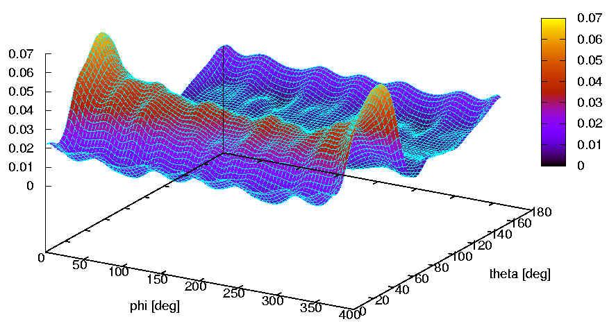
29 More 3D results 29 Ray-trace power (W/stereo-radian) z theta y phi x


30 3D mirror boundaries 30 LED with star-shaped electrode: simulate only ¼ of device with ray-tracing mirror boundaries at x=0 and y=500 um. 3D ray-tracing power including mirror images (in watt/stereoradian) Substantial savings in computation time achieved using mirror boundaries since computation cost scales non-linearly with mesh size.
31 31 Summary The APSYS software has incorporated numerous advanced modules for GaN based LED simulation and design. Rigorous theoretical approaches may be used in all levels of modeling ranging from many-body quantum well theory to 3D transport and ray-tracing. Flexible simulator construction enables various modules to be turned on/off depending on design requirements. Self-consistent integration of various modules within APSYS enables all-in-one simulation approach.
Quantum and Non-local Transport Models in Crosslight Device Simulators. Copyright 2008 Crosslight Software Inc.
 Quantum and Non-local Transport Models in Crosslight Device Simulators Copyright 2008 Crosslight Software Inc. 1 Introduction Quantization effects Content Self-consistent charge-potential profile. Space
Electron leakage effects on GaN-based light-emitting diodes
 Opt Quant Electron (2010) 42:89 95 DOI 10.1007/s11082-011-9437-z Electron leakage effects on GaN-based light-emitting diodes Joachim Piprek Simon Li Received: 22 September 2010 / Accepted: 9 January 2011
Carrier Loss Analysis for Ultraviolet Light-Emitting Diodes
 Carrier Loss Analysis for Ultraviolet Light-Emitting Diodes Joachim Piprek, Thomas Katona, Stacia Keller, Steve DenBaars, and Shuji Nakamura Solid State Lighting and Display Center University of California
Crosslight Software Overview, New Features & Updates. Dr. Peter Mensz
 1 Crosslight Software Overview, New Features & Updates Dr. Peter Mensz 2 Device Simulators Lastip/Pics3d Laser diode FEM models in 2D/3D Apsys 2D and 3D Any other compound semiconductors device FEM models,
Simulation of GaN-based Light-Emitting Devices
 Simulation of GaN-based Light-Emitting Devices Joachim Piprek Solid-State Lighting and Display Center Materials Department, College of Engineering University of California, Santa Barbara, CA 93106 piprek@ieee.org
GaN-based Devices: Physics and Simulation
 GaN-based Devices: Physics and Simulation Joachim Piprek NUSOD Institute Collaborators Prof. Shuji Nakamura, UCSB Prof. Steve DenBaars, UCSB Dr. Stacia Keller, UCSB Dr. Tom Katona, now at S-ET Inc. Dr.
ρ ρ LED access resistances d A W d s n s p p p W the output window size p-layer d p series access resistance d n n-layer series access resistance
 LED access resistances W the output window size p-layer series access resistance d p n-layer series access resistance d n The n-layer series access resistance R = ρ s n where the resistivity of the n-layer
Introduction to Optoelectronic Device Simulation by Joachim Piprek
 NUSOD 5 Tutorial MA Introduction to Optoelectronic Device Simulation by Joachim Piprek Outline:. Introduction: VCSEL Example. Electron Energy Bands 3. Drift-Diffusion Model 4. Thermal Model 5. Gain/Absorption
(b) Spontaneous emission. Absorption, spontaneous (random photon) emission and stimulated emission.
 Spontaneous emission. Absorption, spontaneous (random photon) emission and stimulated emission.") Lecture 10 Stimulated Emission Devices Lasers Stimulated emission and light amplification Einstein coefficients Optical fiber amplifiers Gas laser and He-Ne Laser The output spectrum of a gas laser Laser
Lecture 10 Stimulated Emission Devices Lasers Stimulated emission and light amplification Einstein coefficients Optical fiber amplifiers Gas laser and He-Ne Laser The output spectrum of a gas laser Laser
Chapter 5. Semiconductor Laser
 Chapter 5 Semiconductor Laser 5.0 Introduction Laser is an acronym for light amplification by stimulated emission of radiation. Albert Einstein in 1917 showed that the process of stimulated emission must
Stimulated Emission Devices: LASERS
 Stimulated Emission Devices: LASERS 1. Stimulated Emission and Photon Amplification E 2 E 2 E 2 hυ hυ hυ In hυ Out hυ E 1 E 1 E 1 (a) Absorption (b) Spontaneous emission (c) Stimulated emission The Principle
Final Exam Solution, Spring Semester 2011 ECSE 6962, Light Emitting Diodes and Solid State Lighting (Prof. E. F. Schubert)
") Final Exam Solution, Spring Semester 2011 ECSE 6962, Light Emitting Diodes and Solid State Lighting (Prof. E. F. Schubert) Note: Put your name on your paper. Show your work. Underline all results. Always
Final Exam Solution, Spring Semester 2011 ECSE 6962, Light Emitting Diodes and Solid State Lighting (Prof. E. F. Schubert) Note: Put your name on your paper. Show your work. Underline all results. Always
Advantages of the Blue InGaN/GaN Light-Emitting Diodes with an AlGaN/GaN/AlGaN Quantum Well Structured Electron Blocking Layer
 pubs.acs.org/journal/apchd5 Advantages of the Blue InGaN/GaN Light-Emitting Diodes with an AlGaN/GaN/AlGaN Quantum Well Structured Electron Blocking Layer Zhen Gang Ju, Wei Liu, Zi-Hui Zhang, Swee Tiam
Physics of Semiconductors
 Physics of Semiconductors 9 th 2016.6.13 Shingo Katsumoto Department of Physics and Institute for Solid State Physics University of Tokyo Site for uploading answer sheet Outline today Answer to the question
Ultrafast single photon emitting quantum photonic structures. based on a nano-obelisk
 Ultrafast single photon emitting quantum photonic structures based on a nano-obelisk Je-Hyung Kim, Young-Ho Ko, Su-Hyun Gong, Suk-Min Ko, Yong-Hoon Cho Department of Physics, Graduate School of Nanoscience
Simulation of Quantum Cascade Lasers
 Lighting up the Semiconductor World Simulation of Quantum Cascade Lasers 2005-2010 Crosslight Software Inc. Lighting up the Semiconductor World A A Contents Microscopic rate equation approach Challenge
CHAPTER 2 PHYSICS OF LEDS
 CHAPTER 2 PHYSICS OF LEDS 2.1 LIGHT EMITTING DIODE A light-emitting diode (LED) is simply a two terminal p-n junction diode, which emits light when forward bias is applied across the terminals. When an
Emission Spectra of the typical DH laser
 Emission Spectra of the typical DH laser Emission spectra of a perfect laser above the threshold, the laser may approach near-perfect monochromatic emission with a spectra width in the order of 1 to 10
Final Report for Army Research Office (ARO) and Dr. John Zavada. Report title:
 and Dr. John Zavada. Report title:") Final Report for Army Research Office (ARO) and Dr. John Zavada Report title: GaN light-emitting triodes (LETs) for high-efficiency hole injection and for assessment of the physical origin of the efficiency
Final Report for Army Research Office (ARO) and Dr. John Zavada Report title: GaN light-emitting triodes (LETs) for high-efficiency hole injection and for assessment of the physical origin of the efficiency
This document is downloaded from DR-NTU, Nanyang Technological University Library, Singapore.
 This document is downloaded from DR-NTU, Nanyang Technological University Library, Singapore. Title Author(s) Citation Advantages of the Blue InGaN/GaN Light-Emitting Diodes with an AlGaN/GaN/AlGaN Quantum
Electronic and Optoelectronic Properties of Semiconductor Structures
 Electronic and Optoelectronic Properties of Semiconductor Structures Jasprit Singh University of Michigan, Ann Arbor CAMBRIDGE UNIVERSITY PRESS CONTENTS PREFACE INTRODUCTION xiii xiv 1.1 SURVEY OF ADVANCES
S. Blair February 15,
 S Blair February 15, 2012 66 32 Laser Diodes A semiconductor laser diode is basically an LED structure with mirrors for optical feedback This feedback causes photons to retrace their path back through
Effects of current crowding on light extraction efficiency of conventional GaN-based lightemitting
 Effects of current crowding on light extraction efficiency of conventional GaN-based lightemitting diodes Bin Cao, 1 Shuiming Li, 1 Run Hu, 2 Shengjun Zhou, 3 Yi Sun, 1 Zhiying Gan, 4 and Sheng Liu 4*
External (differential) quantum efficiency Number of additional photons emitted / number of additional electrons injected
 quantum efficiency Number of additional photons emitted / number of additional electrons injected") Semiconductor Lasers Comparison with LEDs The light emitted by a laser is generally more directional, more intense and has a narrower frequency distribution than light from an LED. The external efficiency
Semiconductor Lasers Comparison with LEDs The light emitted by a laser is generally more directional, more intense and has a narrower frequency distribution than light from an LED. The external efficiency
Low efficiency droop of InGaN/GaN blue LEDs with super-lattice active structure
 Low efficiency droop of InGaN/GaN blue LEDs with super-lattice active structure Shih-Pang Chang 1, Kuok-Pan Sou 1, Jet-Rung Chang 2, Yuh-Jen Cheng 1,3, Yuh-Jing Li 2, Yi-Chen Chen 1, Hao-Chung Kuo 1, Ken-Yuh
MTLE-6120: Advanced Electronic Properties of Materials. Semiconductor p-n junction diodes. Reading: Kasap ,
 MTLE-6120: Advanced Electronic Properties of Materials 1 Semiconductor p-n junction diodes Reading: Kasap 6.1-6.5, 6.9-6.12 Metal-semiconductor contact potential 2 p-type n-type p-type n-type Same semiconductor
Potential and Carrier Distribution in AlGaN Superlattice
 Vol. 108 (2005) ACTA PHYSICA POLONICA A No. 4 Proceedings of the XXXIV International School of Semiconducting Compounds, Jaszowiec 2005 Potential and Carrier Distribution in AlGaN Superlattice K.P. Korona,
Organic Device Simulation Using Silvaco Software. Silvaco Taiwan September 2005
 Organic Device Simulation Using Silvaco Software Silvaco Taiwan September 2005 Organic Devices Simulation: Contents Introduction Silvaco TCAD Simulator Theory Models OTFT Simulation v.s Measurement OLED
Optical Investigation of the Localization Effect in the Quantum Well Structures
 Department of Physics Shahrood University of Technology Optical Investigation of the Localization Effect in the Quantum Well Structures Hamid Haratizadeh hamid.haratizadeh@gmail.com IPM, SCHOOL OF PHYSICS,
Spring Semester 2012 Final Exam
 Spring Semester 2012 Final Exam Note: Show your work, underline results, and always show units. Official exam time: 2.0 hours; an extension of at least 1.0 hour will be granted to anyone. Materials parameters
Supplementary Information for
 Supplementary Information for Multi-quantum well nanowire heterostructures for wavelength-controlled lasers Fang Qian 1, Yat Li 1 *, Silvija Gradečak 1, Hong-Gyu Park 1, Yajie Dong 1, Yong Ding 2, Zhong
R. MacKenzie, J.J. Lim, S. Bull, S. Sujecki and E.C. Larkins
 The impact of thermal boundary resistance in opto-electronic devices R. MacKenzie1, J.J. Lim, S. Bull, S. Sujecki and E.C. Larkins School of Electrical and Electronic Engineering, University of Nottingham,
Laser Diodes. Revised: 3/14/14 14: , Henry Zmuda Set 6a Laser Diodes 1
 Laser Diodes Revised: 3/14/14 14:03 2014, Henry Zmuda Set 6a Laser Diodes 1 Semiconductor Lasers The simplest laser of all. 2014, Henry Zmuda Set 6a Laser Diodes 2 Semiconductor Lasers 1. Homojunction
Luminescence basics. Slide # 1
 Luminescence basics Types of luminescence Cathodoluminescence: Luminescence due to recombination of EHPs created by energetic electrons. Example: CL mapping system Photoluminescence: Luminescence due to
Optoelectronics ELEC-E3210
 Optoelectronics ELEC-E3210 Lecture 3 Spring 2017 Semiconductor lasers I Outline 1 Introduction 2 The Fabry-Pérot laser 3 Transparency and threshold current 4 Heterostructure laser 5 Power output and linewidth
THREE-dimensional electronic confinement in semiconductor
 IEEE JOURNAL OF QUANTUM ELECTRONICS, VOL. 43, NO. 3, MARCH 2007 287 Differential Gain and Gain Compression in Quantum-Dot Lasers Andrea Fiore and Alexander Markus Abstract The dynamics of optical gain
Single Photon detectors
 Single Photon detectors Outline Motivation for single photon detection Semiconductor; general knowledge and important background Photon detectors: internal and external photoeffect Properties of semiconductor
Efficient light emission from LEDs, OLEDs, and nanolasers via surface-plasmon resonance
 Efficient light emission from LEDs, OLEDs, and nanolasers via surface-plasmon resonance Seok Ho Song, Hanyang University, http://optics.anyang.ac.kr/~shsong silver grating Key notes 1. How does the surface
Paper Review. Special Topics in Optical Engineering II (15/1) Minkyu Kim. IEEE Journal of Quantum Electronics, Feb 1985
 Minkyu Kim. IEEE Journal of Quantum Electronics, Feb 1985") Paper Review IEEE Journal of Quantum Electronics, Feb 1985 Contents Semiconductor laser review High speed semiconductor laser Parasitic elements limitations Intermodulation products Intensity noise Large
Paper Review IEEE Journal of Quantum Electronics, Feb 1985 Contents Semiconductor laser review High speed semiconductor laser Parasitic elements limitations Intermodulation products Intensity noise Large
Noise in voltage-biased scaled semiconductor laser diodes
 Noise in voltage-biased scaled semiconductor laser diodes S. M. K. Thiyagarajan and A. F. J. Levi Department of Electrical Engineering University of Southern California Los Angeles, California 90089-1111
INSTITUTE BECKMAN. K. Hess, Y. Liu, F. Oyafuso, W.C. Ng and B.D. Klein. The Beckman Institute University of Illinois at Urbana-Champaign
 BECKMAN INSTITUTE K. Hess, Y. Liu, F. Oyafuso, W.C. Ng and B.D. Klein. The Beckman Institute University of Illinois at Urbana-Champaign Photo by Don Hamerman Typical VCSEL Structure and Electronic Mesh
Intraband emission of GaN quantum dots at λ =1.5 μm via resonant Raman scattering
 Intraband emission of GaN quantum dots at λ =1.5 μm via resonant Raman scattering L. Nevou, F. H. Julien, M. Tchernycheva, J. Mangeney Institut d Electronique Fondamentale, UMR CNRS 8622, University Paris-Sud
Hole injection and electron overflow improvement in InGaN/GaN light-emitting diodes by a tapered AlGaN electron blocking layer
 Hole injection and electron overflow improvement in InGaN/GaN light-emitting diodes by a tapered AlGaN electron blocking layer Bing-Cheng Lin, Kuo-Ju Chen, Chao-Hsun Wang, Ching-Hsueh Chiu, 2 Yu-Pin Lan,
Optical Gain Analysis of Strain Compensated InGaN- AlGaN Quantum Well Active Region for Lasers Emitting at nm
 Optical Gain Analysis of Strain Compensated InGaN- AlGaN Quantum Well Active Region for Lasers Emitting at 46-5 nm ongping Zhao, Ronald A. Arif, Yik-Khoon Ee, and Nelson Tansu ±, Department of Electrical
10 GaN-based Light-Emitting Diodes
 10 GaN-based Light-Emitting Diodes J. Piprek 1 and S. Li 2 1 University of California, Santa Barbara, CA 93106-9560, U.S.A., piprek@ieee.org 2 Crosslight Software, 202-3855 Henning Dr., Burnaby, BC V5C
A STUDY OF DYNAMIC CHARACTERIZATIONS OF GaAs/ALGaAs SELF-ASSEMBLED QUANTUM DOT LASERS
 Romanian Reports in Physics, Vol. 63, No. 4, P. 1061 1069, 011 A STUDY OF DYNAMIC CHARACTERIZATIONS OF GaAs/ALGaAs SELF-ASSEMBLED QUANTUM DOT LASERS H. ARABSHAHI Payame Nour University of Fariman, Department
Diode Lasers and Photonic Integrated Circuits
 Diode Lasers and Photonic Integrated Circuits L. A. COLDREN S. W. CORZINE University of California Santa Barbara, California A WILEY-INTERSCIENCE PUBLICATION JOHN WILEY & SONS, INC. NEW YORK / CHICHESTER
Optical properties of strain-compensated hybrid InGaN/InGaN/ZnO quantum well lightemitting
 Optical properties of strain-compensated hybrid InGaN/InGaN/ZnO quantum well lightemitting diodes S.-H. Park 1, S.-W. Ryu 1, J.-J. Kim 1, W.-P. Hong 1, H.-M Kim 1, J. Park 2, and Y.-T. Lee 3 1 Department
Universal valence-band picture of. the ferromagnetic semiconductor GaMnAs
 Universal valence-band picture of the ferromagnetic semiconductor GaMnAs Shinobu Ohya *, Kenta Takata, and Masaaki Tanaka Department of Electrical Engineering and Information Systems, The University of
Effect of non-uniform distribution of electric field on diffusedquantum well lasers
 Title Effect of non-uniform distribution of electric field on diffusedquantum well lasers Author(s) Man, WM; Yu, SF Citation IEEE Hong Kong Electron Devices Meeting Proceedings, Hong Kong, China, 29 August
Thermal performance investigation of DQW GaInNAs laser diodes
 Thermal performance investigation of DQW GaInNAs laser diodes Jun Jun Lim, Roderick MacKenzie, Slawomir Sujecki, Eric Larkins Photonic and Radio Frequency Engineering Group, School of Electrical and Electronic
FIBER OPTICS. Prof. R.K. Shevgaonkar. Department of Electrical Engineering. Indian Institute of Technology, Bombay. Lecture: 14.
 FIBER OPTICS Prof. R.K. Shevgaonkar Department of Electrical Engineering Indian Institute of Technology, Bombay Lecture: 14 Optical Sources Fiber Optics, Prof. R.K. Shevgaonkar, Dept. of Electrical Engineering,
Chapter 6: Light-Emitting Diodes
 Chapter 6: Light-Emitting Diodes Photoluminescence and electroluminescence Basic transitions Luminescence efficiency Light-emitting diodes Internal quantum efficiency External quantum efficiency Device
Sheng S. Li. Semiconductor Physical Electronics. Second Edition. With 230 Figures. 4) Springer
 Springer") Sheng S. Li Semiconductor Physical Electronics Second Edition With 230 Figures 4) Springer Contents Preface 1. Classification of Solids and Crystal Structure 1 1.1 Introduction 1 1.2 The Bravais Lattice
Sheng S. Li Semiconductor Physical Electronics Second Edition With 230 Figures 4) Springer Contents Preface 1. Classification of Solids and Crystal Structure 1 1.1 Introduction 1 1.2 The Bravais Lattice
Effects of transverse mode coupling and optical confinement factor on gallium-nitride based laser diode
 Effects of transverse mode coupling and optical confinement factor on gallium-nitride based laser diode Jin Xiao-Ming( ) a)b), Zhang Bei( ) a) Dai Tao( ) a), and Zhang Guo-Yi( ) a) a) School of Physics
ISSN Review. Progress to a Gallium-Arsenide Deep-Center Laser
 Materials 2009, 2, 1599-1635; doi:10.3390/ma2041599 OPEN ACCESS materials ISSN 1996-1944 www.mdpi.com/journal/materials Review Progress to a Gallium-Arsenide Deep-Center Laser Janet L. Pan Yale University,
Semiconductor device structures are traditionally divided into homojunction devices
 0. Introduction: Semiconductor device structures are traditionally divided into homojunction devices (devices consisting of only one type of semiconductor material) and heterojunction devices (consisting
Multiband GaN/AlGaN UV Photodetector
 Vol. 110 (2006) ACTA PHYSICA POLONICA A No. 2 Proceedings of the XXXV International School of Semiconducting Compounds, Jaszowiec 2006 Multiband GaN/AlGaN UV Photodetector K.P. Korona, A. Drabińska, K.
InAs/GaSb Mid-Wave Cascaded Superlattice Light Emitting Diodes
 InAs/GaSb Mid-Wave Cascaded Superlattice Light Emitting Diodes John Prineas Department of Physics and Astronomy, University of Iowa May 3, 206 Collaborator: Thomas Boggess Grad Students: Yigit Aytak Cassandra
POLITECNICO DI TORINO Repository ISTITUZIONALE
 POLITECICO DI TORIO Repository ISTITUZIOALE DETAILED DRIFT DIFFUSIO MODEL FOR THE AALYSIS AD DESIG OF QUATUM DOT SOLAR CELLS Original DETAILED DRIFT DIFFUSIO MODEL FOR THE AALYSIS AD DESIG OF QUATUM DOT
EE 6313 Homework Assignments
 EE 6313 Homework Assignments 1. Homework I: Chapter 1: 1.2, 1.5, 1.7, 1.10, 1.12 [Lattice constant only] (Due Sept. 1, 2009). 2. Homework II: Chapter 1, 2: 1.17, 2.1 (a, c) (k = π/a at zone edge), 2.3
Course overview. Me: Dr Luke Wilson. The course: Physics and applications of semiconductors. Office: E17 open door policy
 Course overview Me: Dr Luke Wilson Office: E17 open door policy email: luke.wilson@sheffield.ac.uk The course: Physics and applications of semiconductors 10 lectures aim is to allow time for at least one
Simulation Studies of a phosphor-free Monolithic Multi- Wavelength Light-Emitting diode
 Simulation Studies of a phosphor-free Monolithic Multi- Wavelength Light-Emitting diode Sidra Jabeen 1, Shahzad Hussain 2, and Sana Zainab 1 1 CEME, National University of Sciences and Technology (NUST),
Introduction to Sources: Radiative Processes and Population Inversion in Atoms, Molecules, and Semiconductors Atoms and Molecules
 OPTI 500 DEF, Spring 2012, Lecture 2 Introduction to Sources: Radiative Processes and Population Inversion in Atoms, Molecules, and Semiconductors Atoms and Molecules Energy Levels Every atom or molecule
Nonradiative recombination critical in choosing quantum well number for InGaN/GaN light-emitting diodes
 Nonradiative recombination critical in choosing quantum well number for InGaN/GaN light-emitting diodes Yi Ping Zhang, 1 Zi-Hui Zhang, 1 Wei Liu, 1 Swee Tiam Tan, 1 Zhen Gang Ju, 1 Xue Liang Zhang, 1 Yun
Schottky Rectifiers Zheng Yang (ERF 3017,
 ECE442 Power Semiconductor Devices and Integrated Circuits Schottky Rectifiers Zheng Yang (ERF 3017, email: yangzhen@uic.edu) Power Schottky Rectifier Structure 2 Metal-Semiconductor Contact The work function
THE DEVELOPMENT OF SIMULATION MODEL OF CARRIER INJECTION IN QUANTUM DOT LASER SYSTEM
 THE DEVELOPMENT OF SIMULATION MODEL OF CARRIER INJECTION IN QUANTUM DOT LASER SYSTEM Norbaizura Nordin 1 and Shahidan Radiman 2 1 Centre for Diploma Studies Universiti Tun Hussein Onn Malaysia 1,2 School
Semiconductor Physics and Devices
 The pn Junction 1) Charge carriers crossing the junction. 3) Barrier potential Semiconductor Physics and Devices Chapter 8. The pn Junction Diode 2) Formation of positive and negative ions. 4) Formation
ECE236A Semiconductor Heterostructure Materials Group III Nitride Semiconductors Lecture 17, Nov. 30, 2017
 ECE236A Semiconductor Heterostructure Materials Group III Nitride Semiconductors Lecture 17, Nov. 30, 2017 Spontaneous and Piezoelectric Polarization Effects on 2DEG in HFETs Effects of Polarization on
Traps in MOCVD n-gan Studied by Deep Level Transient Spectroscopy and Minority Carrier Transient Spectroscopy
 Traps in MOCVD n-gan Studied by Deep Level Transient Spectroscopy and Minority Carrier Transient Spectroscopy Yutaka Tokuda Department of Electrical and Electronics Engineering, Aichi Institute of Technology,
arxiv: v3 [cond-mat.mes-hall] 18 Mar 2017
![arxiv: v3 [cond-mat.mes-hall] 18 Mar 2017](/thumbs/79/79623103.jpg "arxiv: v3 [cond-mat.mes-hall] 18 Mar 2017") Hot Carrier Transportation Dynamics in InAs/GaAs Quantum Dot Solar Cell Tomah Sogabe i-powered Energy Research Center (i-perc), The University of Electro-Communications, Tokyo, Japan Department of Engineering
Hot Carrier Transportation Dynamics in InAs/GaAs Quantum Dot Solar Cell Tomah Sogabe i-powered Energy Research Center (i-perc), The University of Electro-Communications, Tokyo, Japan Department of Engineering
Ultrafast carrier dynamics in InGaN MQW laser diode
 Invited Paper Ultrafast carrier dynamics in InGaN MQW laser diode Kian-Giap Gan* a, Chi-Kuang Sun b, John E. Bowers a, and Steven P. DenBaars a a Department of Electrical and Computer Engineering, University
Semiconductor Lasers II
 Semiconductor Lasers II Materials and Structures Edited by Eli Kapon Institute of Micro and Optoelectronics Department of Physics Swiss Federal Institute oftechnology, Lausanne OPTICS AND PHOTONICS ACADEMIC
MSE 310/ECE 340: Electrical Properties of Materials Fall 2014 Department of Materials Science and Engineering Boise State University
 MSE 310/ECE 340: Electrical Properties of Materials Fall 2014 Department of Materials Science and Engineering Boise State University Practice Final Exam 1 Read the questions carefully Label all figures
Title: Ultrafast photocurrent measurement of the escape time of electrons and holes from
 Title: Ultrafast photocurrent measurement of the escape time of electrons and holes from carbon nanotube PN junction photodiodes Authors: Nathaniel. M. Gabor 1,*, Zhaohui Zhong 2, Ken Bosnick 3, Paul L.
Semiconductor Physical Electronics
 Semiconductor Physical Electronics Sheng S. Li Department of Electrical Engineering University of Florida Gainesville, Florida Plenum Press New York and London Contents CHAPTER 1. Classification of Solids
Ballistic Electron Spectroscopy of Quantum Mechanical Anti-reflection Coatings for GaAs/AlGaAs Superlattices
 Ballistic Electron Spectroscopy of Quantum Mechanical Anti-reflection Coatings for GaAs/AlGaAs Superlattices C. Pacher, M. Kast, C. Coquelin, G. Fasching, G. Strasser, E. Gornik Institut für Festkörperelektronik,
Si - Based Tunnel Diode Operation and Forecasted Performance
 Si - Based Tunnel Diode Operation and Forecasted Performance Roger Lake Raytheon Systems Dallas, TX Si / Si x Ge -x Interband Tunnel Diodes The main tunneling process is LA and TO phonon assisted tunneling
De De. De M Q fix = const PR R/R Intensity (arb. inits) Energy (ev) a) b)
 Energy (ev) a) b)") PIEZOELECTRIC EFFECTS IN GaInN/GaN HETEROSTRUCTURES AND QUANTUM WELLS C. WETZEL, T. TAKEUCHI, S. YAMAGUCHI, H. KATO, H. AMANO, and I. AKASAKI High Tech Research Center, Meijo University, 1-501 Shiogamaguchi,
PIEZOELECTRIC EFFECTS IN GaInN/GaN HETEROSTRUCTURES AND QUANTUM WELLS C. WETZEL, T. TAKEUCHI, S. YAMAGUCHI, H. KATO, H. AMANO, and I. AKASAKI High Tech Research Center, Meijo University, 1-501 Shiogamaguchi,
Physics of Semiconductors 8 th
 Physics of Semiconductors 8 th 2016.6.6 Shingo Katsumoto Department of Physics, Institute for Solid State Physics University of Tokyo Review of pn junction Estimation of builtin potential Depletion layer
School of Electrical and Computer Engineering, Cornell University. ECE 5330: Semiconductor Optoelectronics. Fall 2014
 School of Electrical and Computer Engineering, Cornell University ECE 5330: Semiconductor Optoelectronics Fall 014 Homework 7 Due on Nov. 06, 014 Suggested Readings: i) Study lecture notes. ii) Study Coldren
Solar Cell Materials and Device Characterization
 Solar Cell Materials and Device Characterization April 3, 2012 The University of Toledo, Department of Physics and Astronomy SSARE, PVIC Principles and Varieties of Solar Energy (PHYS 4400) and Fundamentals
EE 472 Solutions to some chapter 4 problems
 EE 472 Solutions to some chapter 4 problems 4.4. Erbium doped fiber amplifier An EDFA is pumped at 1480 nm. N1 and N2 are the concentrations of Er 3+ at the levels E 1 and E 2 respectively as shown in
Microscopic Modelling of the Optical Properties of Quantum-Well Semiconductor Lasers
 Microscopic Modelling of the Optical Properties of Quantum-Well Semiconductor Lasers Stephan W. Koch Department of Physics Philipps University, Marburg/Germany OVERVIEW - Outline of Theory - Gain/Absorption
Influence of the quantum well models on the numerical simulation of planar InGaN/GaN LED results
 Journal of Physics: Conference Series PAPER OPEN ACCESS Influence of the quantum well models on the numerical simulation of planar InGaN/GaN LED results To cite this article: J Podgórski et al 2016 J.
Segmented 1.55um Laser with 400% Differential Quantum Efficiency J. Getty, E. Skogen, L. Coldren, University of California, Santa Barbara, CA.
 Segmented 1.55um Laser with 400% Differential Quantum Efficiency J. Getty, E. Skogen, L. Coldren, University of California, Santa Barbara, CA. Abstract: By electrically segmenting, and series-connecting
Metal Vapour Lasers Use vapoured metal as a gain medium Developed by W. Silfvast (1966) Two types: Ionized Metal vapour (He-Cd) Neutral Metal vapour
 Two types: Ionized Metal vapour (He-Cd) Neutral Metal vapour") Metal Vapour Lasers Use vapoured metal as a gain medium Developed by W. Silfvast (1966) Two types: Ionized Metal vapour (He-Cd) Neutral Metal vapour (Cu) All operate by vaporizing metal in container Helium
Metal Vapour Lasers Use vapoured metal as a gain medium Developed by W. Silfvast (1966) Two types: Ionized Metal vapour (He-Cd) Neutral Metal vapour (Cu) All operate by vaporizing metal in container Helium
Optically-Pumped Ge-on-Si Gain Media: Lasing and Broader Impact
 Optically-Pumped Ge-on-Si Gain Media: Lasing and Broader Impact J. Liu 1, R. Camacho 2, X. Sun 2, J. Bessette 2, Y. Cai 2, X. X. Wang 1, L. C. Kimerling 2 and J. Michel 2 1 Thayer School, Dartmouth College;
CME 300 Properties of Materials. ANSWERS: Homework 9 November 26, As atoms approach each other in the solid state the quantized energy states:
 CME 300 Properties of Materials ANSWERS: Homework 9 November 26, 2011 As atoms approach each other in the solid state the quantized energy states: are split. This splitting is associated with the wave
- Outline. Chapter 4 Optical Source. 4.1 Semiconductor physics
 Chapter 4 Optical Source - Outline 4.1 Semiconductor physics - Energy band - Intrinsic and Extrinsic Material - pn Junctions - Direct and Indirect Band Gaps 4. Light Emitting Diodes (LED) - LED structure
White Rose Research Online URL for this paper:
 This is a repository copy of Self-consistent solutions to the intersubband rate equations in quantum cascade lasers: Analysis of a GaAs/AlxGa1-xAs device. White Rose Research Online URL for this paper:
Basic Principles of Light Emission in Semiconductors
 Basic Principles of Light Emission in Semiconductors Class: Integrated Photonic Devices Time: Fri. 8:00am ~ 11:00am. Classroom: 資電 06 Lecturer: Prof. 李明昌 (Ming-Chang Lee) Model for Light Generation and
A PN-type quantum barrier for InGaN/GaN light emitting diodes
 A PN-type quantum barrier for InGaN/GaN light emitting diodes Zi-Hui Zhang, 1 Swee Tiam Tan, 1 Yun Ji, 1 Wei Liu, 1 Zhengang Ju, 1 Zabu Kyaw, 1 Xiao Wei Sun 1,2,5 and Hilmi Volkan Demir 1,3,4,* 1 LUMINOUS!
Lecture 2. Introduction to semiconductors Structures and characteristics in semiconductors
 Lecture 2 Introduction to semiconductors Structures and characteristics in semiconductors Semiconductor p-n junction Metal Oxide Silicon structure Semiconductor contact Literature Glen F. Knoll, Radiation
TANDEM BLUE-VIOLET QUANTUM WELL InGaN LASERS WITH HIGH-FREQUENCY SELF-PULSATIONS. I. Antohi, S. Rusu, and V. Z. Tronciu
 TANDEM BLUE-VIOLET QUANTUM WELL InGaN LASERS WITH HIGH-FREQUENCY SELF-PULSATIONS I. Antohi, S. Rusu, and V. Z. Tronciu Department of Physics, Technical University of Moldova, Chisinau, MD2004 Republic
Current mechanisms Exam January 27, 2012
 Current mechanisms Exam January 27, 2012 There are four mechanisms that typically cause currents to flow: thermionic emission, diffusion, drift, and tunneling. Explain briefly which kind of current mechanisms
GaN light-emitting triodes for high-efficiency hole injection and light emission
 GaN light-emitting triodes for high-efficiency hole injection and light emission Jong Kyu Kim a,*, J.-Q. Xi a, Hong Luo a, Jaehee Cho b, Cheolsoo Sone b, Yongjo Park b, Thomas Gessmann a, J. M. Zavada
(a) (b) Supplementary Figure 1. (a) (b) (a) Supplementary Figure 2. (a) (b) (c) (d) (e)
 (b) Supplementary Figure 1. (a) (b) (a) Supplementary Figure 2. (a) (b) (c) (d) (e)") (a) (b) Supplementary Figure 1. (a) An AFM image of the device after the formation of the contact electrodes and the top gate dielectric Al 2 O 3. (b) A line scan performed along the white dashed line
(a) (b) Supplementary Figure 1. (a) An AFM image of the device after the formation of the contact electrodes and the top gate dielectric Al 2 O 3. (b) A line scan performed along the white dashed line
Ge Quantum Well Modulators on Si. D. A. B. Miller, R. K. Schaevitz, J. E. Roth, Shen Ren, and Onur Fidaner
 10.1149/1.2986844 The Electrochemical Society Ge Quantum Well Modulators on Si D. A. B. Miller, R. K. Schaevitz, J. E. Roth, Shen Ren, and Onur Fidaner Ginzton Laboratory, 450 Via Palou, Stanford CA 94305-4088,