Microscopic Modelling of the Optical Properties of Quantum-Well Semiconductor Lasers
|
|
|
- Constance Barber
- 6 years ago
- Views:
Transcription
1 Microscopic Modelling of the Optical Properties of Quantum-Well Semiconductor Lasers Stephan W. Koch Department of Physics Philipps University, Marburg/Germany OVERVIEW - Outline of Theory - Gain/Absorption - Luminescence - Radiative and Auger Losses - Nonequilibrium Effects COLLABORATORS - A. Thränhardt, I. Kutzentsova, S.Becker, Marburg - J. Hader, J. V. Moloney et al., Tucson - W. Chow, Sandia SUPPORT - AFOSR F , DFG
2 Overview simple models: easy to use often poorly controlled, ad hoc assumptions rely on major experimental input (semi-)empirical fits of experimental data many and adjustable parameters limited potential for predictions. microscopic theory: numerically demanding systematic approach based on fundamental physics controlled approximations predicts experiments no need for detailed experimental input wide range of applicability can be used as basis for controllably simplified models.


3 Semiconductor Optics: Semiclassical Theory MAXWELL S WAVE EQUATION macroscopic optical polarization semiconductors: Bloch basis general theory: Haug/Koch, Quantum Theory of the Optical and Electronic Properties of Semiconductors, 4th ed., World Scientific (2004)


4 Semiconductor Density Matrix two-band model, one QW subband e-h-pair transition amplitude occupation probabilities

5 Hamiltonian H = H 0 + H Coul + H dip H 0 single particle (band structure) H Coul Coulomb interaction between carriers H dip dipole interaction with optical field
6 Calculation of Optical Response Heisenberg equation of motion: structure of resulting equations: infinite hierarchy of many-body correlations systematic CLUSTER expansion


7 Schematics of Cluster Expansion two-point level (uncorrelated single particles) four-point level (two particle correlations)


8 Semiconductor Bloch Equations all contributions beyond singlets HF field renormalization HF energy renormalization nonlinearities: phase-space filling, gap reduction, Coulomb enhancement correlation contributions: scattering, dephasing, screening

9 Second Born-Markov Approximation intraband Coulomb scattering phonon scattering Born-Markov limit: Boltzmann equation Coulomb scattering phonon scattering
10 scattering rates: Coulomb Scattering I


11 Coulomb Scattering II quasi-equilibrium: detailed balance Fermi-Dirac distribution:
12 Excitation Induced Dephasing Re Γ k (t) diagonal dephasing generalized T 2 time Im Γ k (t) diagonal energy shift generalized band-gap shift Re ( ) off-diagonal dephasing Γ k, k ' t Im ( ) off-diagonal energy shift Γ k, k ' t and are calculated from all terms quadratic in the screened Coulomb interaction strong compensation between diagonal and off-diagonal terms important for excitation saturation: Jahnke et al., PRL 77, 5257 (1996). and gain calculations: Chow/Koch, Semiconductor-Laser Fundamentals, Springer Verlag (1999).
 Detuning Absorption experiment: InGaAs/GaAs")
 EID first observed in 4-wave mixing, Wang et al.")
13 Density Dependent Absorption F. Jahnke, M. Kira, and S.W. Koch, Z. Physik B 104, 559 (1997) Detuning Absorption experiment: InGaAs/GaAs QW Khitrova, Gibbs, Jahnke, Kira, Koch, Rev. Mod. Phys. 71, 1591 (1999) EID first observed in 4-wave mixing, Wang et al. PRL 71, 1261 (1993)
![Lineshape Problem 0.2 Absorption [10 3 /cm] 0.0-0.2-0.4 dephasing rate approx. full calculation -0.](/docs-images/80/80502139/images/14-1.jpg "6-20 -10 0 Detuning 10 gain of two-band bulk material nondiagonal scattering contributions lineshape modification, no absorption below the gap Hughes, Knorr,")
14 Lineshape Problem 0.2 Absorption [10 3 /cm] dephasing rate approx. full calculation Detuning 10 gain of two-band bulk material nondiagonal scattering contributions lineshape modification, no absorption below the gap Hughes, Knorr, Koch, Binder, Indik, and Moloney Solid State Comm. 100, 555 (1996)
15 Optical Gain: Theory and Experiment 10nm (9.2nm) InGaAs/AlGaAs absorption/gain absorption (x10 3 /cm) absorption/gain [1/cm] Detuning N=1.6, 2.2, 2.5, 3.0*10 12 /cm 2 exp: D. Bossert et al., theory: A. Girndt et al., Marburg 8nm InGaAs/AlGaAs 6.8 nm In 0.4 Ga 0.5 P/(Al 0.5 Ga 0.5 )In 0.51 P 0.49 Detuning Current 0-20mA Density x10 12 cm -2 exp: C. Ellmers et al., theory: A. Girndt et al. Marburg Photon Energy (ev) Courtesy of W.W. Chow, P.M. Smowton, P. Blood, A. Grindt, F. Jahnke, and S.W. Koch
16 Wide Bandgap Materials: InGaN/GaN 2nm In 0. 2Ga 0. 8N / GaN, T = 300 K 5 8 nm In0. 2Ga0. As / GaAs, T = 300K 4-1 TE absorption (10 cm ) cm 2 unexcited qw bandgap unexcited qw bandgap cm Photon Energy (ev) cm Photon Energy (ev) strong Coulomb effects: gapshift and broadening excitonic effects even at elevated densities and temperatures


17 Semiconductor Luminescence where is proportional to dipole matrix element and mode strength at the QW position
18 Semiconductor Luminescence Equations I photon operator dynamics polarization operator dynamics Coulomb hierarchy problem (as in semiclassical theory) photon-carrier coupling hierarchy Cluster expansion to treat hierarchies on equal footing
19 Semiconductor Luminescence Equations II photon assisted interband polarization incoherent source coherent source feedback (cavity) excitonic signatures


20 Quasi Stationary: Luminescence Elliott Equation with true excitons excitonic resonances independent of source term relative peak height depends on populations PRL 92, (2004)

21 Gain/Absorption and Luminescence 5nm Ga 0.8 In 0.2 As/GaAs pin-mqw gain: theory: 1.0, 1.125, 1.25, 1.375, 1.5, 1.625, 1.75, PL: theory: 0.17, 0.30, 0.40, 0.53, 0.68, 0.86 [10 12 / cm 2 ] experiment: 6.0, 6.5, 7.0, 7.5, 8.3, 9.0 [ma] experiment: 12, 16, 18, 21, 24 [mw]
22 Luminescence Analysis Input: nominal structural parameters experimental luminescence spectra at two moderate intensities Analysis: calculate ideal, homogeneously broadened luminescence spectra for given structure compare to experimental luminescence determine from deviations the inhomogeneous broadening, actual structural parameters, quality of device use optimized parameters to calculate gain/absorption spectra, refractive index, differential gain, linewidth enhancement factor, Ref.: Hader et al., IEEE Phot. Techn. Lett. 14, 762 (2002)
As/GaAs sandwiched between n and p doped buffer layers experiment: 12, 16, 18, 21, 24 mw theory: 0.1, 0.17, 0.23, 0.3, 0.4, 0.53, 0.68, 0.")
23 Luminescence Analysis II sample with three quantum wells nominal composition: 5nm Ga(.8)In(.2)As/GaAs sandwiched between n and p doped buffer layers experiment: 12, 16, 18, 21, 24 mw theory: 0.1, 0.17, 0.23, 0.3, 0.4, 0.53, 0.68, cm 2 no broadening, no shifting needed: slight adjustment of composition inhomogeneous broadening
24 Luminescence Analysis Input: nominal structural parameters experimental luminescence spectra at two moderate intensities Analysis: calculate ideal, homogeneously broadened luminescence spectra for given structure compare to experimental luminescence determine from deviations the inhomogeneous broadening, actual structural parameters, quality of device
As/GaAs sandwiched between n and p doped buffer layers experiment: 12, 16, 18, 21, 24 mw theory: 0.1, 0.17, 0.23, 0.3, 0.4, 0.53, 0.68, 0.")
25 Luminescence Analysis III sample with three quantum wells nominal composition: 5nm Ga(.8)In(.2)As/GaAs sandwiched between n and p doped buffer layers experiment: 12, 16, 18, 21, 24 mw theory: 0.1, 0.17, 0.23, 0.3, 0.4, 0.53, 0.68, cm 2 good fit to experiment yields actual composition less In (0.19) or thinner (- one monolayer)
26 Luminescence Analysis Input: nominal structural parameters experimental luminescence spectra at two moderate intensities Analysis: calculate ideal, homogeneously broadened luminescence spectra for given structure compare to experimental luminescence determine from deviations the inhomogeneous broadening, actual structural parameters, quality of device use optimized parameters to calculate gain/absorption spectra

27 Absorption/Gain using optimized material parameters experimental inhomogeneous broadening theory: 0.5, 0.75, 1.0, 1.25,, 4.25, 4.5 [10 12 /cm 2 ] modal absorption [1/cm] wavelength [nm] other results: refractive index, alfa parameter, etc.
![Test of Predicted Gain Spectra independently measured gain spectra NO additional fitting! experiment: 5.0, 6.0, 6.5, 7.0, 7.5, 8.0, 8.6, 10.0 [mv] theory: 1.](/docs-images/80/80502139/images/28-0.jpg "0, 1.125, 1.25, 1.375, 1.5, 1.625, 1.75, 1.875 [10 12 cm 2 ] very good theory/experiment agreement verification of microscopic theory predictive capabilities")
28 Test of Predicted Gain Spectra independently measured gain spectra NO additional fitting! experiment: 5.0, 6.0, 6.5, 7.0, 7.5, 8.0, 8.6, 10.0 [mv] theory: 1.0, 1.125, 1.25, 1.375, 1.5, 1.625, 1.75, [10 12 cm 2 ] very good theory/experiment agreement verification of microscopic theory predictive capabilities
29 Losses in Semiconductor Lasers Classical Parametrization of Loss Current J loss : defect-recombination spontaneous emission Auger recombination non-capture, escape E E E hω k k k usually negligible in high quality crystal growth usually dominant absent in optically pumped devices Problems with A, B, C - Parametrization: parameters only very roughly known and only for special cases; depend on well- and barrier-materials, layer widths, temperatures, densities... simple density-dependence far from reality


30 Spontaneous Recombination Current: Examples increases only linear with N at high densities
31 Auger Recombination I E k Inclusion of particle number non-conserving terms: Impact Ionization Auger Recombination


32 Auger Recombination II Quantum-Boltzmann scattering in 2. Born-Markov approximation: Impact Ionization Auger Recombination


33 Auger Recombination: Examples increases far less than cubic with N sometimes even less than quadratic
34 Theory-Experiment Comparison I Theoretical Procedure: calculate gain for various densities search for density that overcomes intrinsic losses (mirror losses) = threshold density calculate spontaneous emission and Auger recombination for this density comparison with experimental data without adjustment (experimental data from R.Fehse, et al., IEEE J. Sel. Topics Quantum Electron. 8, 801 (2002))
35 Theory-Experiment Comparison II experimental data: A.F. Phillips et al., IEEE J. Sel. Topics Quantum Electron. 5, 401 (1999))
36 Laser Modelling: VECSEL Vertical External Cavity Surface Emitting Laser Numerical simulation issues: optical pumping = input of carriers and kinetic energy nonequilibrium carrier distributions, nonequilibrium gain dynamic response..
37 Nonequilibrium Gain Simulations Semiconductor Bloch Equations Reduced Wave Equation Full numerical solution way too time consuming APPROACH Calculate rates for scattering/relaxation/dephasing Solve coupled equations Interesting situations: pulsed and/or CW excitation
38 Relaxation Rate Model for Scattering Parameters Relaxation rates are obtained by fits to microscopic calculations is calculated considering energy and particle conservation is calculated considering particle conservation Carrier-carrier scattering is an order of magnitude faster than carrier-phonon scattering Band structure is taken from microscopic calculations
39 Carrier Dynamics Electron Density fs 0fs 100fs 250fs 500fs optical excitation Energy (mev) 10nm Ga In As QW between 20.3nm GaN As 0.993, Excitation by a 50fs pulse at 1.35eV at t=0
40 Effective Carrier-Carrier Scattering Times f k,peak -f Fermi Microscopic Calculation Exponential Fit, τ = 349fs Time (fs) simple evaluation exponential fits work well
41 Electron-Hole Scattering Times Electron scattering times τ (fs) Hole scattering times Excitation Energy (ev) Hole scattering faster because of larger effective mass (Initial Density 2.0*10 12 /cm -2 ) Variation of scattering times with excitation energy (band structure vs availability of scattering partners) Increased scattering time for lower densities (e.g. for 1.5 * cm -2 e = 354 fs, h = 94 fs, instead of e = 349 fs, h = 87 fs at 2.0 * cm -2 )
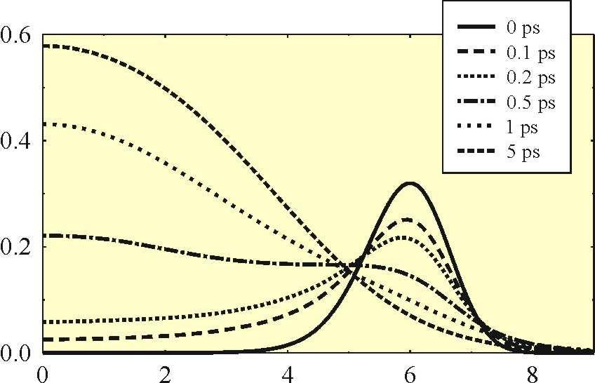
42 Switch-On of Optically Pumped SCL dynamics of electron and hole distributions Electron Distribution kinetic hole 2.5ps 5ps 25ps 175ps optical excitation Hole Distribution ps 5ps 25ps 175ps Energy (ev) Energy (ev) distinct kinetic hole in electron distribution small kinetic hole in hole distribution due to faster scattering time
43 Gain Dynamics ps 5ps 25ps 175ps cw gain αl initial absorption turns into gain transient gain overshoot Energy (ev)
44 Carrier Temperature and Laser Intensity 16 Intracavity Intensity (MW/cm 2 ) Time (ps) Temperature (K) Plasma Temperature Electron Temperature Hole Temperature 383K 379K 372K Time (ps)
45 Excitation Induced Temperature Change T = (E exc -E gap )/k T (K) *10 12 cm *10 12 cm Excitation Energy (ev) hot carriers (relative to the bandgap) can still cool down carrier distribution excitation energy = 0.61 ev => Excitation at energy chemical potential => T=0 hole chemical potential always in the bandgap E exc
46 Summary predictive microscopic theory application to semiconductor laser gain media luminescence, Auger loss rates nonequilibrium gain, laser dynamics MANY CHALLENGES: non-classical properties (quantum optics, quantum information science, ) modified photonic environment (phot. x-tals, ) microscopic modelling of disorder References and more informations: (look for: semiconductor theory)
Optics and Quantum Optics with Semiconductor Nanostructures. Overview
 Optics and Quantum Optics with Semiconductor Nanostructures Stephan W. Koch Department of Physics, Philipps University, Marburg/Germany and Optical Sciences Center, University of Arizona, Tucson/AZ Overview
Summary lecture VI. with the reduced mass and the dielectric background constant
 Summary lecture VI Excitonic binding energy reads with the reduced mass and the dielectric background constant Δ Statistical operator (density matrix) characterizes quantum systems in a mixed state and
Luminescence Process
 Luminescence Process The absorption and the emission are related to each other and they are described by two terms which are complex conjugate of each other in the interaction Hamiltonian (H er ). In an
Semiconductor-Laser Fundamentals
 Semiconductor-Laser Fundamentals Springer-Verlag Berlin Heidelberg GmbH Weng W. Chow Stephan W. Koch Semiconductor-laser Fundamentals Physics of the Gain Materials With 132 Figures and 3 Tables Springer
Energy Band Calculations for Dynamic Gain Models in Semiconductor Quantum Well Lasers
 Energy Band Calculations for Dynamic Gain Models in School of Electrical and Electronic Engineering University of Nottingham; Nottingham NG7 2RD; UK Email: eexpjb1@nottingham.ac.uk Presentation Outline
Optical Properties of Semiconductors. Prof.P. Ravindran, Department of Physics, Central University of Tamil Nadu, India
 Optical Properties of Semiconductors 1 Prof.P. Ravindran, Department of Physics, Central University of Tamil Nadu, India http://folk.uio.no/ravi/semi2013 Light Matter Interaction Response to external electric
Optical Properties of Solid from DFT
 Optical Properties of Solid from DFT 1 Prof.P. Ravindran, Department of Physics, Central University of Tamil Nadu, India & Center for Materials Science and Nanotechnology, University of Oslo, Norway http://folk.uio.no/ravi/cmt15
Summary lecture VII. Boltzmann scattering equation reads in second-order Born-Markov approximation
 Summary lecture VII Boltzmann scattering equation reads in second-order Born-Markov approximation and describes time- and momentum-resolved electron scattering dynamics in non-equilibrium Markov approximation
Electromagnetically Induced Transparency (EIT) via Spin Coherences in Semiconductor
 via Spin Coherences in Semiconductor") Electromagnetically Induced Transparency (EIT) via Spin Coherences in Semiconductor Hailin Wang Oregon Center for Optics, University of Oregon, USA Students: Shannon O Leary Susanta Sarkar Yumin Shen Phedon
Electromagnetically Induced Transparency (EIT) via Spin Coherences in Semiconductor Hailin Wang Oregon Center for Optics, University of Oregon, USA Students: Shannon O Leary Susanta Sarkar Yumin Shen Phedon
Electronic and Optoelectronic Properties of Semiconductor Structures
 Electronic and Optoelectronic Properties of Semiconductor Structures Jasprit Singh University of Michigan, Ann Arbor CAMBRIDGE UNIVERSITY PRESS CONTENTS PREFACE INTRODUCTION xiii xiv 1.1 SURVEY OF ADVANCES
Non-equilibrium Green s functions: Rough interfaces in THz quantum cascade lasers
 Non-equilibrium Green s functions: Rough interfaces in THz quantum cascade lasers Tillmann Kubis, Gerhard Klimeck Department of Electrical and Computer Engineering Purdue University, West Lafayette, Indiana
Quantum Theory of the Optical and Electronic Properties of Semiconductors Downloaded from
 This page intentionally left blank Published by World Scientific Publishing Co. Pte. Ltd. 5 Toh Tuck Link, Singapore 596224 USA office: 27 Warren Street, Suite 401-402, Hackensack, NJ 07601 UK office:
M R S Internet Journal of Nitride Semiconductor Research
 M R S Internet Journal of Nitride Semiconductor Research Volume 2, Article 25 Properties of the Biexciton and the Electron-Hole-Plasma in Highly Excited GaN J.-Chr. Holst, L. Eckey, A. Hoffmann, I. Broser
(Al,In)GaN laser diodes in spectral, spatial, and time domain: near-field measurements and basic simulations
GaN laser diodes in spectral, spatial, and time domain: near-field measurements and basic simulations") (Al,In)GaN laser diodes in spectral, spatial, and time domain: near-field measurements and basic simulations Ulrich Schwarz Department of Experimental and Applied Physics Regensburg University Optical
(Al,In)GaN laser diodes in spectral, spatial, and time domain: near-field measurements and basic simulations Ulrich Schwarz Department of Experimental and Applied Physics Regensburg University Optical
Laser Physics OXFORD UNIVERSITY PRESS SIMON HOOKER COLIN WEBB. and. Department of Physics, University of Oxford
 Laser Physics SIMON HOOKER and COLIN WEBB Department of Physics, University of Oxford OXFORD UNIVERSITY PRESS Contents 1 Introduction 1.1 The laser 1.2 Electromagnetic radiation in a closed cavity 1.2.1
Quantum design of semiconductor active materials: laser and amplifier applications
 24 Laser & Photon. Rev. 1, No. 1, 24 43 (2007) / DOI 10.1002/lpor.200610003 Abstract: We present an overview of a novel first-principles quantum approach to designing and optimizing semiconductor quantum-well
Intensity / a.u. 2 theta / deg. MAPbI 3. 1:1 MaPbI 3-x. Cl x 3:1. Supplementary figures
 Intensity / a.u. Supplementary figures 110 MAPbI 3 1:1 MaPbI 3-x Cl x 3:1 220 330 0 10 15 20 25 30 35 40 45 2 theta / deg Supplementary Fig. 1 X-ray Diffraction (XRD) patterns of MAPbI3 and MAPbI 3-x Cl
Optical Investigation of the Localization Effect in the Quantum Well Structures
 Department of Physics Shahrood University of Technology Optical Investigation of the Localization Effect in the Quantum Well Structures Hamid Haratizadeh hamid.haratizadeh@gmail.com IPM, SCHOOL OF PHYSICS,
Introduction to Optoelectronic Device Simulation by Joachim Piprek
 NUSOD 5 Tutorial MA Introduction to Optoelectronic Device Simulation by Joachim Piprek Outline:. Introduction: VCSEL Example. Electron Energy Bands 3. Drift-Diffusion Model 4. Thermal Model 5. Gain/Absorption
Luminescence basics. Slide # 1
 Luminescence basics Types of luminescence Cathodoluminescence: Luminescence due to recombination of EHPs created by energetic electrons. Example: CL mapping system Photoluminescence: Luminescence due to
SUPPLEMENTARY INFORMATION
 doi:10.1038/nature12036 We provide in the following additional experimental data and details on our demonstration of an electrically pumped exciton-polariton laser by supplementing optical and electrical
Ultrafast Spectroscopy of Semiconductors and Semiconductor Nanostructures
 Springer Series in Solid-State Sciences 115 Ultrafast Spectroscopy of Semiconductors and Semiconductor Nanostructures Bearbeitet von Jagdeep Shah erweitert 1999. Buch. xvi, 522 S. Hardcover ISBN 978 3
Basic Principles of Light Emission in Semiconductors
 Basic Principles of Light Emission in Semiconductors Class: Integrated Photonic Devices Time: Fri. 8:00am ~ 11:00am. Classroom: 資電 06 Lecturer: Prof. 李明昌 (Ming-Chang Lee) Model for Light Generation and
arxiv: v2 [cond-mat.mes-hall] 6 Apr 2011
![arxiv: v2 [cond-mat.mes-hall] 6 Apr 2011](/thumbs/72/66469363.jpg "arxiv: v2 [cond-mat.mes-hall] 6 Apr 2011") Electron spin relaxation as evidence of excitons in a two dimensional electron-hole plasma arxiv:1103.2474v2 [cond-mat.mes-hall] 6 Apr 2011 S. Oertel, 1 S. Kunz, 1 D. Schuh, 2 W. Wegscheider, 3 J. Hübner,
Electron spin relaxation as evidence of excitons in a two dimensional electron-hole plasma arxiv:1103.2474v2 [cond-mat.mes-hall] 6 Apr 2011 S. Oertel, 1 S. Kunz, 1 D. Schuh, 2 W. Wegscheider, 3 J. Hübner,
THREE-dimensional electronic confinement in semiconductor
 IEEE JOURNAL OF QUANTUM ELECTRONICS, VOL. 43, NO. 3, MARCH 2007 287 Differential Gain and Gain Compression in Quantum-Dot Lasers Andrea Fiore and Alexander Markus Abstract The dynamics of optical gain
Summary lecture IX. The electron-light Hamilton operator reads in second quantization
 Summary lecture IX The electron-light Hamilton operator reads in second quantization Absorption coefficient α(ω) is given by the optical susceptibility Χ(ω) that is determined by microscopic polarization
Optical Properties of Lattice Vibrations
 Optical Properties of Lattice Vibrations For a collection of classical charged Simple Harmonic Oscillators, the dielectric function is given by: Where N i is the number of oscillators with frequency ω
Intersubband Response:
 Intersubband Response: Lineshape,, Coulomb Renormalization, and Microcavity Effects F. T. Vasko Inst. of Semiconductor Physics Kiev, Ukraine In collaboration with: A.V. Korovin and O.E. Raichev (Inst.
Emission Spectra of the typical DH laser
 Emission Spectra of the typical DH laser Emission spectra of a perfect laser above the threshold, the laser may approach near-perfect monochromatic emission with a spectra width in the order of 1 to 10
Chapter 5. Semiconductor Laser
 Chapter 5 Semiconductor Laser 5.0 Introduction Laser is an acronym for light amplification by stimulated emission of radiation. Albert Einstein in 1917 showed that the process of stimulated emission must
Optical Nonlinearities in Quantum Wells
 Harald Schneider Institute of Ion-Beam Physics and Materials Research Semiconductor Spectroscopy Division Rosencher s Optoelectronic Day Onéra 4.05.011 Optical Nonlinearities in Quantum Wells Harald Schneider
Excitonic luminescence upconversion in a two-dimensional semiconductor
 Excitonic luminescence upconversion in a two-dimensional semiconductor Authors: Aaron M. Jones 1, Hongyi Yu 2, John R. Schaibley 1, Jiaqiang Yan 3,4, David G. Mandrus 3-5, Takashi Taniguchi 6, Kenji Watanabe
Electrically Driven Polariton Devices
 Electrically Driven Polariton Devices Pavlos Savvidis Dept of Materials Sci. & Tech University of Crete / FORTH Polariton LED Rome, March 18, 211 Outline Polariton LED device operating up to room temperature
External (differential) quantum efficiency Number of additional photons emitted / number of additional electrons injected
 quantum efficiency Number of additional photons emitted / number of additional electrons injected") Semiconductor Lasers Comparison with LEDs The light emitted by a laser is generally more directional, more intense and has a narrower frequency distribution than light from an LED. The external efficiency
Semiconductor Lasers Comparison with LEDs The light emitted by a laser is generally more directional, more intense and has a narrower frequency distribution than light from an LED. The external efficiency
(b) Spontaneous emission. Absorption, spontaneous (random photon) emission and stimulated emission.
 Spontaneous emission. Absorption, spontaneous (random photon) emission and stimulated emission.") Lecture 10 Stimulated Emission Devices Lasers Stimulated emission and light amplification Einstein coefficients Optical fiber amplifiers Gas laser and He-Ne Laser The output spectrum of a gas laser Laser
Lecture 10 Stimulated Emission Devices Lasers Stimulated emission and light amplification Einstein coefficients Optical fiber amplifiers Gas laser and He-Ne Laser The output spectrum of a gas laser Laser
Electron-phonon interaction. Can dispersionless phonons provide relaxation?
 Electron-phonon interaction. Can dispersionless phonons provide relaxation? P. Gartner, J. Seebeck, F. Jahnke Institute for Theoretical Physics University of Bremen Kiel, 21 Introduction Self-assembled
Stimulated Emission Devices: LASERS
 Stimulated Emission Devices: LASERS 1. Stimulated Emission and Photon Amplification E 2 E 2 E 2 hυ hυ hυ In hυ Out hυ E 1 E 1 E 1 (a) Absorption (b) Spontaneous emission (c) Stimulated emission The Principle
Chapter 2 Optical Transitions
 Chapter 2 Optical Transitions 2.1 Introduction Among energy states, the state with the lowest energy is most stable. Therefore, the electrons in semiconductors tend to stay in low energy states. If they
Dynamical Condensation of ExcitonPolaritons
 ICSCE 2008 Dynamical Condensation of ExcitonPolaritons Y. Yamamoto, H. Deng, G. Weihs, C.W. Lai, G. Roumpos and S. Utsunomiya Stanford University and National Institute of Informatics Loeffler, S. Hoefling,
Intraband emission of GaN quantum dots at λ =1.5 μm via resonant Raman scattering
 Intraband emission of GaN quantum dots at λ =1.5 μm via resonant Raman scattering L. Nevou, F. H. Julien, M. Tchernycheva, J. Mangeney Institut d Electronique Fondamentale, UMR CNRS 8622, University Paris-Sud
Many-Body Coulomb Effects in the Optical Properties of Semiconductor Heterostructures
 John von Neumann Institute for Computing Many-Body Coulomb Effects in the Optical Properties of Semiconductor Heterostructures Torsten Meier, Bernhard Pasenow, Peter Thomas, Stephan W. Koch published in
Elements of Quantum Optics
 Pierre Meystre Murray Sargent III Elements of Quantum Optics Fourth Edition With 124 Figures fya Springer Contents 1 Classical Electromagnetic Fields 1 1.1 Maxwell's Equations in a Vacuum 2 1.2 Maxwell's
Transient Intersubband Optical Absorption in Double Quantum Well Structure
 Commun. Theor. Phys. (Beijing, China) 43 (2005) pp. 759 764 c International Academic Publishers Vol. 43, No. 4, April 15, 2005 Transient Intersubband Optical Absorption in Double Quantum Well Structure
Polariton Condensation
 Polariton Condensation Marzena Szymanska University of Warwick Windsor 2010 Collaborators Theory J. Keeling P. B. Littlewood F. M. Marchetti Funding from Macroscopic Quantum Coherence Macroscopic Quantum
Multilevel Infrared Coupling of Excitons in Quantum-Well Semiconductors
 IEEE JOURNAL OF QUANTUM ELECTRONICS, VOL. 36, NO. 11, NOVEMBER 2000 1267 Multilevel Infrared Coupling of Excitons in Quantum-Well Semiconductors S. M. Sadeghi, J. Meyer, T. Tiedje, and M. Beaudoin Abstract
Exciton spectroscopy
 Lehrstuhl Werkstoffe der Elektrotechnik Exciton spectroscopy in wide bandgap semiconductors Lehrstuhl Werkstoffe der Elektrotechnik (WW6), Universität Erlangen-Nürnberg, Martensstr. 7, 91058 Erlangen Vortrag
Fundamentals of Spectroscopy for Optical Remote Sensing. Course Outline 2009
 Fundamentals of Spectroscopy for Optical Remote Sensing Course Outline 2009 Part I. Fundamentals of Quantum Mechanics Chapter 1. Concepts of Quantum and Experimental Facts 1.1. Blackbody Radiation and
LIST OF TOPICS BASIC LASER PHYSICS. Preface xiii Units and Notation xv List of Symbols xvii
 ate LIST OF TOPICS Preface xiii Units and Notation xv List of Symbols xvii BASIC LASER PHYSICS Chapter 1 An Introduction to Lasers 1.1 What Is a Laser? 2 1.2 Atomic Energy Levels and Spontaneous Emission
Optically-Pumped Ge-on-Si Gain Media: Lasing and Broader Impact
 Optically-Pumped Ge-on-Si Gain Media: Lasing and Broader Impact J. Liu 1, R. Camacho 2, X. Sun 2, J. Bessette 2, Y. Cai 2, X. X. Wang 1, L. C. Kimerling 2 and J. Michel 2 1 Thayer School, Dartmouth College;
Time Resolved Pump-Probe Reflectivity in GaAs and GaN
 Time Resolved Pump-Probe Reflectivity in GaAs and GaN S. S. Prabhu * and A. S. Vengurlekar Department of Condensed Matter Physics and Material Science, Tata Institute of Fundamental Research, Homi Bhabha
Diode Lasers and Photonic Integrated Circuits
 Diode Lasers and Photonic Integrated Circuits L. A. COLDREN S. W. CORZINE University of California Santa Barbara, California A WILEY-INTERSCIENCE PUBLICATION JOHN WILEY & SONS, INC. NEW YORK / CHICHESTER
ISSN Review. Progress to a Gallium-Arsenide Deep-Center Laser
 Materials 2009, 2, 1599-1635; doi:10.3390/ma2041599 OPEN ACCESS materials ISSN 1996-1944 www.mdpi.com/journal/materials Review Progress to a Gallium-Arsenide Deep-Center Laser Janet L. Pan Yale University,
Terahertz Lasers Based on Intersubband Transitions
 Terahertz Lasers Based on Intersubband Transitions Personnel B. Williams, H. Callebaut, S. Kumar, and Q. Hu, in collaboration with J. Reno Sponsorship NSF, ARO, AFOSR,and NASA Semiconductor quantum wells
Resonantly Excited Time-Resolved Photoluminescence Study of Self-Organized InGaAs/GaAs Quantum Dots
 R. Heitz et al.: PL Study of Self-Organized InGaAs/GaAs Quantum Dots 65 phys. stat. sol. b) 221, 65 2000) Subject classification: 73.61.Ey; 78.47.+p; 78.55.Cr; 78.66.Fd; S7.12 Resonantly Excited Time-Resolved
Polariton laser in micropillar cavities
 Polariton laser in micropillar cavities D. Bajoni, E. Wertz, P. Senellart, I. Sagnes, S. Bouchoule, A. Miard, E. Semenova, A. Lemaître and J. Bloch Laboratoire de Photonique et de Nanostructures LPN/CNRS,
Sheng S. Li. Semiconductor Physical Electronics. Second Edition. With 230 Figures. 4) Springer
 Springer") Sheng S. Li Semiconductor Physical Electronics Second Edition With 230 Figures 4) Springer Contents Preface 1. Classification of Solids and Crystal Structure 1 1.1 Introduction 1 1.2 The Bravais Lattice
Sheng S. Li Semiconductor Physical Electronics Second Edition With 230 Figures 4) Springer Contents Preface 1. Classification of Solids and Crystal Structure 1 1.1 Introduction 1 1.2 The Bravais Lattice
A STUDY OF DYNAMIC CHARACTERIZATIONS OF GaAs/ALGaAs SELF-ASSEMBLED QUANTUM DOT LASERS
 Romanian Reports in Physics, Vol. 63, No. 4, P. 1061 1069, 011 A STUDY OF DYNAMIC CHARACTERIZATIONS OF GaAs/ALGaAs SELF-ASSEMBLED QUANTUM DOT LASERS H. ARABSHAHI Payame Nour University of Fariman, Department
(002)(110) (004)(220) (222) (112) (211) (202) (200) * * 2θ (degree)
(110) (004)(220) (222) (112) (211) (202) (200) * * 2θ (degree)") Supplementary Figures. (002)(110) Tetragonal I4/mcm Intensity (a.u) (004)(220) 10 (112) (211) (202) 20 Supplementary Figure 1. X-ray diffraction (XRD) pattern of the sample. The XRD characterization indicates
Supplementary Figures. (002)(110) Tetragonal I4/mcm Intensity (a.u) (004)(220) 10 (112) (211) (202) 20 Supplementary Figure 1. X-ray diffraction (XRD) pattern of the sample. The XRD characterization indicates
Mutual transparency of coherent laser beams through a terahertz-field-driven quantum well
 A. Maslov and D. Citrin Vol. 19, No. 8/August 2002/J. Opt. Soc. Am. B 1905 Mutual transparency of coherent laser beams through a terahertz-field-driven quantum well Alexey V. Maslov and D. S. Citrin School
Ultrafast All-optical Switches Based on Intersubband Transitions in GaN/AlN Multiple Quantum Wells for Tb/s Operation
 Ultrafast All-optical Switches Based on Intersubband Transitions in GaN/AlN Multiple Quantum Wells for Tb/s Operation Jahan M. Dawlaty, Farhan Rana and William J. Schaff Department of Electrical and Computer
interband transitions in semiconductors M. Fox, Optical Properties of Solids, Oxford Master Series in Condensed Matter Physics
 interband transitions in semiconductors M. Fox, Optical Properties of Solids, Oxford Master Series in Condensed Matter Physics interband transitions in quantum wells Atomic wavefunction of carriers in
doi: /PhysRevLett
 doi: 10.1103/PhysRevLett.77.494 Luminescence Hole Burning and Quantum Size Effect of Charged Excitons in CuCl Quantum Dots Tadashi Kawazoe and Yasuaki Masumoto Institute of Physics and Center for TARA
Metal Vapour Lasers Use vapoured metal as a gain medium Developed by W. Silfvast (1966) Two types: Ionized Metal vapour (He-Cd) Neutral Metal vapour
 Two types: Ionized Metal vapour (He-Cd) Neutral Metal vapour") Metal Vapour Lasers Use vapoured metal as a gain medium Developed by W. Silfvast (1966) Two types: Ionized Metal vapour (He-Cd) Neutral Metal vapour (Cu) All operate by vaporizing metal in container Helium
Metal Vapour Lasers Use vapoured metal as a gain medium Developed by W. Silfvast (1966) Two types: Ionized Metal vapour (He-Cd) Neutral Metal vapour (Cu) All operate by vaporizing metal in container Helium
Quantum Feedback Stabilized Solid-State Emitters
 FOPS 2015 Breckenridge, Colorado Quantum Feedback Stabilized Solid-State Emitters Alexander Carmele, Julia Kabuss, Sven Hein, Franz Schulze, and Andreas Knorr Technische Universität Berlin August 7, 2015
Soft Carrier Multiplication by Hot Electrons in Graphene
 Soft Carrier Multiplication by Hot Electrons in Graphene Anuj Girdhar 1,3 and J.P. Leburton 1,2,3 1) Department of Physics 2) Department of Electrical and Computer Engineering, and 3) Beckman Institute
INSTITUTE BECKMAN. K. Hess, Y. Liu, F. Oyafuso, W.C. Ng and B.D. Klein. The Beckman Institute University of Illinois at Urbana-Champaign
 BECKMAN INSTITUTE K. Hess, Y. Liu, F. Oyafuso, W.C. Ng and B.D. Klein. The Beckman Institute University of Illinois at Urbana-Champaign Photo by Don Hamerman Typical VCSEL Structure and Electronic Mesh
Noise in voltage-biased scaled semiconductor laser diodes
 Noise in voltage-biased scaled semiconductor laser diodes S. M. K. Thiyagarajan and A. F. J. Levi Department of Electrical Engineering University of Southern California Los Angeles, California 90089-1111
LASERS. Amplifiers: Broad-band communications (avoid down-conversion)
") L- LASERS Representative applications: Amplifiers: Broad-band communications (avoid down-conversion) Oscillators: Blasting: Energy States: Hydrogen atom Frequency/distance reference, local oscillators,
L- LASERS Representative applications: Amplifiers: Broad-band communications (avoid down-conversion) Oscillators: Blasting: Energy States: Hydrogen atom Frequency/distance reference, local oscillators,
Simple strategy for enhancing terahertz emission from coherent longitudinal optical phonons using undoped GaAs/n-type GaAs epitaxial layer structures
 Presented at ISCS21 June 4, 21 Session # FrP3 Simple strategy for enhancing terahertz emission from coherent longitudinal optical phonons using undoped GaAs/n-type GaAs epitaxial layer structures Hideo
Signal regeneration - optical amplifiers
 Signal regeneration - optical amplifiers In any atom or solid, the state of the electrons can change by: 1) Stimulated absorption - in the presence of a light wave, a photon is absorbed, the electron is
Simulation of Quantum Cascade Lasers
 Lighting up the Semiconductor World Simulation of Quantum Cascade Lasers 2005-2010 Crosslight Software Inc. Lighting up the Semiconductor World A A Contents Microscopic rate equation approach Challenge
Supplementary Information
 Ultrafast Dynamics of Defect-Assisted Electron-Hole Recombination in Monolayer MoS Haining Wang, Changjian Zhang, and Farhan Rana School of Electrical and Computer Engineering, Cornell University, Ithaca,
Supplementary Information for
 Supplementary Information for Multi-quantum well nanowire heterostructures for wavelength-controlled lasers Fang Qian 1, Yat Li 1 *, Silvija Gradečak 1, Hong-Gyu Park 1, Yajie Dong 1, Yong Ding 2, Zhong
Semiconductor Physical Electronics
 Semiconductor Physical Electronics Sheng S. Li Department of Electrical Engineering University of Florida Gainesville, Florida Plenum Press New York and London Contents CHAPTER 1. Classification of Solids
Electron leakage effects on GaN-based light-emitting diodes
 Opt Quant Electron (2010) 42:89 95 DOI 10.1007/s11082-011-9437-z Electron leakage effects on GaN-based light-emitting diodes Joachim Piprek Simon Li Received: 22 September 2010 / Accepted: 9 January 2011
Carrier Loss Analysis for Ultraviolet Light-Emitting Diodes
 Carrier Loss Analysis for Ultraviolet Light-Emitting Diodes Joachim Piprek, Thomas Katona, Stacia Keller, Steve DenBaars, and Shuji Nakamura Solid State Lighting and Display Center University of California
Laser Diodes. Revised: 3/14/14 14: , Henry Zmuda Set 6a Laser Diodes 1
 Laser Diodes Revised: 3/14/14 14:03 2014, Henry Zmuda Set 6a Laser Diodes 1 Semiconductor Lasers The simplest laser of all. 2014, Henry Zmuda Set 6a Laser Diodes 2 Semiconductor Lasers 1. Homojunction
Optoelectronics ELEC-E3210
 Optoelectronics ELEC-E3210 Lecture 3 Spring 2017 Semiconductor lasers I Outline 1 Introduction 2 The Fabry-Pérot laser 3 Transparency and threshold current 4 Heterostructure laser 5 Power output and linewidth
Fermi polaron-polaritons in MoSe 2
 Fermi polaron-polaritons in MoSe 2 Meinrad Sidler, Patrick Back, Ovidiu Cotlet, Ajit Srivastava, Thomas Fink, Martin Kroner, Eugene Demler, Atac Imamoglu Quantum impurity problem Nonperturbative interaction
Review of Optical Properties of Materials
 Review of Optical Properties of Materials Review of optics Absorption in semiconductors: qualitative discussion Derivation of Optical Absorption Coefficient in Direct Semiconductors Photons When dealing
PHYSICS OF SEMICONDUCTORS AND THEIR HETEROSTRUCTURES
 PHYSICS OF SEMICONDUCTORS AND THEIR HETEROSTRUCTURES Jasprit Singh University of Michigan McGraw-Hill, Inc. New York St. Louis San Francisco Auckland Bogota Caracas Lisbon London Madrid Mexico Milan Montreal
White Rose Research Online URL for this paper:
 This is a repository copy of Self-consistent solutions to the intersubband rate equations in quantum cascade lasers: Analysis of a GaAs/AlxGa1-xAs device. White Rose Research Online URL for this paper:
Quantum Nanoplasmonics and the Spaser
 Photo Credit: I. Tsukerman, Seefeld, Austria, January, Department 2009 of Physics and Astronomy US Israel Binational Science Foundation Quantum Nanoplasmonics and the Spaser Mark I. Stockman Department
Investigation of Optical Nonlinearities and Carrier Dynamics in In-Rich InGaN Alloys
 Vol. 113 (2008) ACTA PHYSICA POLONICA A No. 3 Proceedings of the 13th International Symposium UFPS, Vilnius, Lithuania 2007 Investigation of Optical Nonlinearities and Carrier Dynamics in In-Rich InGaN
EE 472 Solutions to some chapter 4 problems
 EE 472 Solutions to some chapter 4 problems 4.4. Erbium doped fiber amplifier An EDFA is pumped at 1480 nm. N1 and N2 are the concentrations of Er 3+ at the levels E 1 and E 2 respectively as shown in
REPORT DOCUMENTATION PAGE
 REPORT DOCUMENTATION PAGE Form Approved OMB No. 74-88 Public reporting burden for this collection of information is estimated to average hour per response, including the time for reviewing instructions,
Thermal performance investigation of DQW GaInNAs laser diodes
 Thermal performance investigation of DQW GaInNAs laser diodes Jun Jun Lim, Roderick MacKenzie, Slawomir Sujecki, Eric Larkins Photonic and Radio Frequency Engineering Group, School of Electrical and Electronic
Microcavity Exciton-Polariton
 Microcavity Exciton-Polariton Neil Na ( 那允中 ) Institute of Photonics Technologies National Tsing-Hua University 5/3/2012 Outline Microcavity Exciton-polariton QW excitons Microcavity photons Strong coupling
Magnetostatic modulation of nonlinear refractive index and absorption in quantum wires
 Superlattices and Microstructures, Vol. 23, No. 6, 998 Article No. sm96258 Magnetostatic modulation of nonlinear refractive index and absorption in quantum wires A. BALANDIN, S.BANDYOPADHYAY Department
Temperature Dependent Optical Band Gap Measurements of III-V films by Low Temperature Photoluminescence Spectroscopy
 Temperature Dependent Optical Band Gap Measurements of III-V films by Low Temperature Photoluminescence Spectroscopy Linda M. Casson, Francis Ndi and Eric Teboul HORIBA Scientific, 3880 Park Avenue, Edison,
Theoretical investigation on intrinsic linewidth of quantum cascade lasers. Liu Tao
 Theoretical investigation on intrinsic linewidth of quantum cascade lasers Liu Tao School of Electrical and Electronic Engineering 014 Theoretical investigation on intrinsic linewidth of quantum cascade
Carrier Recombination
 Notes for ECE-606: Spring 013 Carrier Recombination Professor Mark Lundstrom Electrical and Computer Engineering Purdue University, West Lafayette, IN USA lundstro@purdue.edu /19/13 1 carrier recombination-generation
PRINCIPLES OF NONLINEAR OPTICAL SPECTROSCOPY
 PRINCIPLES OF NONLINEAR OPTICAL SPECTROSCOPY Shaul Mukamel University of Rochester Rochester, New York New York Oxford OXFORD UNIVERSITY PRESS 1995 Contents 1. Introduction 3 Linear versus Nonlinear Spectroscopy
Lecture 15: Optoelectronic devices: Introduction
 Lecture 15: Optoelectronic devices: Introduction Contents 1 Optical absorption 1 1.1 Absorption coefficient....................... 2 2 Optical recombination 5 3 Recombination and carrier lifetime 6 3.1
Multiple Exciton Generation in Quantum Dots. James Rogers Materials 265 Professor Ram Seshadri
 Multiple Exciton Generation in Quantum Dots James Rogers Materials 265 Professor Ram Seshadri Exciton Generation Single Exciton Generation in Bulk Semiconductors Multiple Exciton Generation in Bulk Semiconductors
Optical Characterization of Solids
 D. Dragoman M. Dragoman Optical Characterization of Solids With 184 Figures Springer 1. Elementary Excitations in Solids 1 1.1 Energy Band Structure in Crystalline Materials 2 1.2 k p Method 11 1.3 Numerical
Supplementary Figure S1 Definition of the wave vector components: Parallel and perpendicular wave vector of the exciton and of the emitted photons.
 Supplementary Figure S1 Definition of the wave vector components: Parallel and perpendicular wave vector of the exciton and of the emitted photons. Supplementary Figure S2 The calculated temperature dependence
Supplementary Figure 1 Interlayer exciton PL peak position and heterostructure twisting angle. a, Photoluminescence from the interlayer exciton for
 Supplementary Figure 1 Interlayer exciton PL peak position and heterostructure twisting angle. a, Photoluminescence from the interlayer exciton for six WSe 2 -MoSe 2 heterostructures under cw laser excitation
PRESENTED BY: PROF. S. Y. MENSAH F.A.A.S; F.G.A.A.S UNIVERSITY OF CAPE COAST, GHANA.
 SOLAR CELL AND ITS APPLICATION PRESENTED BY: PROF. S. Y. MENSAH F.A.A.S; F.G.A.A.S UNIVERSITY OF CAPE COAST, GHANA. OUTLINE OF THE PRESENTATION Objective of the work. A brief introduction to Solar Cell
Dr. Masahiro Yoshita Inst. for Sol. St. Physics Univ. of Tokyo CREST, JST Kashiwanoha, Kashiwa Chiba , JAPAN. Dear Dr.
 Subject: Your_manuscript LP9512 Yoshita From: Physical Review Letters Date: Tue, 13 Jul 2004 18:56:22 UT To: yoshita@issp.u-tokyo.ac.jp Re: LP9512 Crossover of excitons to an electron-hole