Crosslight Software Overview, New Features & Updates. Dr. Peter Mensz
|
|
|
- Coral Miles
- 5 years ago
- Views:
Transcription
1 1 Crosslight Software Overview, New Features & Updates Dr. Peter Mensz
2 2 Device Simulators Lastip/Pics3d Laser diode FEM models in 2D/3D Apsys 2D and 3D Any other compound semiconductors device FEM models, excluding stimulated emission. E.g. photodetectors, LEDs, HEMTs. APSYS Quantum-MOS 2D and 3D All APSYS features For small L ch ~ < 0.1μm MOSFET with ultra thin oxides ( can include selfconsistent Poisson and Schroedinger Eqs. Solver tunneling, Many Body corrections)
3 Optional Modules and Advanced Features: Quantum Tunneling Option Complex MQW Option Selfconsistent MQW Model VCSEL Option Vectorial Wave Function PML/EEIM Option and Radiative Mode Waveguide Modes of Passive Devices 3D Flow Option ;3D Optical+ 3D flow(elect.+therm.) Semiconductor Optical Amplifier Option Light Emitting Diode Option LED Ray Tracing Option FIBER-Grating/External Cavity Option Travel Wave Optical Amplifier ( for high speed SOA) Second Order Grating Option Beam Propagation Method Option Fiber/External-Cavity Optically Pumped Laser Option Many Body and Exciton Option 8x8 k.p Model Photon-Absorbing Waveguide Option (3D-Simulation for SOA, EAM, WPD) 3
4 Semiconductor Physical Process 4 Simulators PROCOM- 3D Chemical and Fluid Dynamic MOCVD Process Simulator Chemical species distributions in reactor. Gas flow pattern. Temperature distribution. Film deposition rates and composition. Common impurity incorporation. CSUPREM- 3D Semiconductor Processing Simulator physical models for ion implantation, deposition, etching, diffusion, and oxidation. Export doping profiles needed in device simulations. Based on technology licensed from Stanford University (Prof. Robert Dutton s group).
5 Quantum Drift-Diffusion Model In Crosslight Device Simulators 5
6 Introduction:Device evolution Optoelectronic devices: Laser diode: from double heterostructure laser to quantum well laser. LED: from bulk to multiple quantum wells. Silicon IC: CMOS gate length from several microns down to deep submicrons. Semiconductor from pure Si to strained Si on SiGe. Generalized quantum effect: Size effect: quantum confinement; QUNTUM WELLS, QUANTUM DOTS, QUANTUM WIRES Quantum tunneling (intraband and interband). Band structure engineering: strain dependent valley splitting, density of state design, mobility enhancement and optical transition selection. 6
7 Integrated Quantum-Drift-Diffusion Diffusion Model 7 Poisson Equation Electron/Hole Drift-Diffusion Model (Energy transport) Potential profile Space charge Injection current Tunneling current correction Wave Mechanics (Quantization/ Tunneling/ Multi-band k.p Theory)
8 Quantum tunneling correction 8 J TE bar J DD JTE Thermionic emission J DD J DD J TE bar J DD Enhanced by tunneling Factor from quantum Model. Drift-diffusion
9 Demonstration: RTD simulation 9

10 Quantum/classical regions in a MOSFET 10 May also be poly-gate
11 11 Quantum-DD model works!
12 12 Material Properties As Commands Ease of management: Input commands and material parameters completely define a simulation. Material parameters are isolated from numerical calculation. Flexible: Nearly any kind of parameter dependence (temperature, doping, composition) may be implemented or modified by user. Fortran/C syntax and logical control. Numerical tables may also be included in macro.
13 Types of material macros Basic bulk material macro. Strained/unstrained symmetric zincblende quantum well. Strained wurtzite symmetric quantum well. OLED Complex quantum wells (coupled, non-symmetric, type-ii, etc.) Complex MOS quantum well. General complex strained QW (strained silicon QW). 13
14 14 Strained Silicon Complete first principle band Structure model too difficult To be included in 3D drift- Diffusion solver. Use Composition parameterization Instead. Macro needs for all composition range: Strained bandgap for different valleys. DOS masses for each valley, for both perpendicular and parallel directions. Bandgap discontinuity Strained Si on SiGe (Richard et. Al. J. Appl. Phys. Vol. 94,1795 )

Ge(x) on relaxed Si(1-y)Ge(y) (Rieger&Vogl,")
15 15 Parameterization of Strained Silicon Band Structure Δ 2 Δ 4 Δ 4 Δ 2 Implemented in Crosslight material macro library Strained Si(1-x)Ge(x) on relaxed Si(1-y)Ge(y) (Rieger&Vogl, Phys. Rev B48, )

16 Strained Si on Relaxed SiGe 16 Lower valley: smaller parallel mass but larger perpendicular mass. Higher valley: larger parallel mass but smaller perpendicular mass.
17 Complex LD/VCSEL Simulation and Advanced Quantum Well Models. Copyright Crosslight Software Inc. 17
18 18 Contents Multiple section tunable DFB/DBR laser. Fiber/external-cavity lasers Multiple lateral/longitudinal mode simulation. Lateral mode competition in VCSEL. Different k.p theories.
19 19 3-section DBR laser Physical model required: Current injection (driftdiffusion model) for all segments. MQW gain model in segment 1. Index change model in segment 2 & 3. DBR grating model in segment 3 (coupled mode theory). Lateral optical mode solver for all segments. Longitudinal mode model (Green s function theory) for all segments.
20 20 Round trip gain (RTG) RTG left RTG right
21 Longitudinal mode distribution 21 Modeling/Design Issues: Segments 2 & 3 should be close to but below bandgap to avoid optical loss but also to provide change of index. Both waveguide and DBR grating should vary with injection current.
22 Tuning behavior 22 Conclusion Possible to integrate many modules to describe complex laser behavior in 3D spatial and spectral dimensions.
23 Example of fibre grating DBR laser 23 Laser Diode
24 Traveling Waves: 24 Air gap SOA Fiber grating
25 25 Multiple section tunable DFB/DBR laser. Multiple lateral/longitudinal mode simulation. Lateral mode competition in VCSEL. Different k.p theories. Copyright Crosslight Software Inc.
26 Broad-area area laser with adjustable stripe 26 Adjustable twin-stripe for lateral mode control GRIN-SQW Symmetric axis

 Lateral mode No.")
27 Pumping of different modes 27 Injection current magnitude (current spreading) Lateral mode No. 1 Lateral mode No. 2
28 Multi-mode considerations 28 Different longitudinal modes For lateral mode No. 1 Different lateral modes For longitudinal No. 1 Must solve a whole different set of longitudinal modes using modal indices of different lateral modes. Each longitudinal mode is always associated with a particular lateral mode. Must consider longitudinal and lateral spatial hole burning effects for different lateral/longitudinal modes.
29 Multi-lateral lateral mode spectrum 29 Different peaks for different lateral modes. May be used to monitor suppression of lateral modes.
30 30 Multiple section tunable DFB/DBR laser. Multiple lateral/longitudinal mode simulation. Lateral mode competition in VCSEL. Different k.p theories. Copyright Crosslight Software Inc.
31 Reflection symmetry axis Symmetric v. asymmetric VCSEL Top contact Top DBR 31 MQW layers Bottom DBR Bottom contact Models required: Full 3D drift-diffusion model: cylindrical symmetry no longer available. Lateral mode model with both phi and theta dependence. MQW gain model as usual. Transfer matrix model for longitudinal modes as usual.

32 Asymmetric VCSEL injection 32 Current magnitude Contact QW s Fundamental mode QW s 2 nd order mode QW s
33 Mode competition behavor 33 Asymmetric VCSEL Total 2 nd order Symmetric VCSEL Fundamental Total 2 nd order Conclusions a) VCSEL has similar lateral mode competition behavior as edge laser; b) Asymmetric VCSEL mode is necessary to simulate multi-lateral mode behavior. Fundamental
34 34 Multiple section tunable DFB/DBR laser. Multiple lateral/longitudinal mode simulation. Lateral mode competition in VCSEL. Different k.p theories. Copyright Crosslight Software Inc.
35 k.p theories for zinc-blende 35 Subbands from 8x8 k.p theory For GaAs/AlGaAs Motivations: When conventional parabolic gain model does not fit experiment, we need to try something else. Need to determine whether it is worth the trouble to go to higher order k.p theories.
36 Comparison for GaAs/AlGaAs QW 36 QW=GaAs/Al(0.33)Ga(0.67)As (t=76a)
37 Light v. current 37 QW=GaAs/Al(0.33)Ga(0.67)As (t=76a)
As/In(.74)Ga(.26)As(.57)P(.")
38 Comparison for InGaAsP QW 38 QW=InGa(.47)As/In(.74)Ga(.26)As(.57)P(.43) t=60a
39 InGaAsP QW L-I L I curve 39 QW=InGa(.47)As/In(.74)Ga(.26)As(.57)P(.43) t=60a
40 Simulation of InGaN/GaN MQW LED with U-shape Contact Copyright Crosslight Software Inc. 40
41 Structure 41 MQW U-shape Contact
42 42 Physical Models Quantum drift-diffusion model for current flow/spreading (included). MQW quantum well gain/spontaneous emission model with effective mass approximation (included). 3D ray-tracing model (included). K.p model for MQW (optional). Self-heating model (optional). Polarization surface charge/self-consistent model (optional).
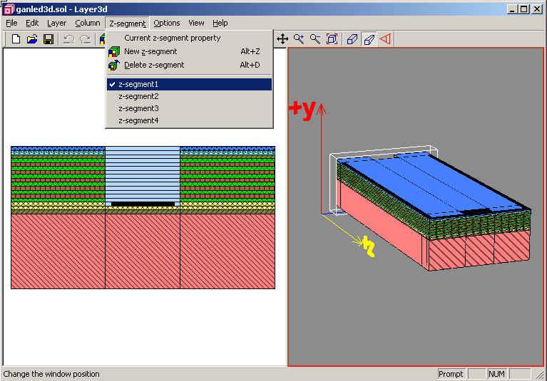
43 Z-segment1 43
44 Z-segment2 44
45 Band Diagram 45 May be viewed at any positions
46 3D View: Current at QW 46

47 3D View: Current below QW 47
48 Raytracing: : emission to the top 48 theta
49 Raytracing: : emission around 49 phi
50 Simulation of an Alq3/TPD OLED Copyright Crosslight Software Inc. 50

51 Structure 51
52 Coordinates 52 Metal Cathode ITO Anode
53 53 Physical Models Quantum drift-diffusion model for current flow/spreading (included). Poole-Frenkel field dependent mobility model (included). Mobility-dependent bi-molecular radiative recombination model (included). 3D ray-tracing model (included). Deep level trap model (included). Quantum tunneling model for Schottky barriers and heterojunctions (optional). Self-heating model (optional).
54 Band Diagram 54 ALQ3 organic material LUMO Fermi levels HOMO TPD organic material Energy band diagram of a OLED of TPD/ALQ3
55 3D Radiative Light Source 55 Material Interface
56 I-V V Curve 56
57 Modeling of Organic Semiconductor Electroluminescent (EL) and Absorption Spectra 57 Organic semiconductor emits light via Frenkel exciton recombination. Conventional semiconductor theories based on free-carrier/many-body interband transition are no longer valid. We have established optical spectrum model based on exciton-phonon interaction within an organic crystal.
58 Some Fitted EL Spectra 58
59 EL Spectrum Model of Alq3:DCM 59 Field=1.E8 Field=1.E7 Applied electric field ranges from 1.E7 to 1.E8 V/m
60 Conclusions Crosslight Software develops indebt 2/3D advance features of Laser, LED Modeling, PIC, along with other Quantum Transport modeling, specifically Quantum MOS for UHLSI CMOS technology. It can be interfaced with CSUPREM, for example with Monte-Carlo implantation modeling New non-semiconductor device modeling was successfully applied to the polymer materials, and OLED devices. New tools for modeling of MOCVD and semiconductor device fabrications will allow for more complementary TCAD design and Interfacing with Device Modeling Software. 60
Quantum and Non-local Transport Models in Crosslight Device Simulators. Copyright 2008 Crosslight Software Inc.
 Quantum and Non-local Transport Models in Crosslight Device Simulators Copyright 2008 Crosslight Software Inc. 1 Introduction Quantization effects Content Self-consistent charge-potential profile. Space
Computer Aided Design of GaN Light-Emitting Diodes. Copyright 2006 Crosslight Software Inc.
 Computer Aided Design of GaN Light-Emitting Diodes Copyright 2006 Crosslight Software Inc. www.crosslight.com 1 2 Contents Available tools and modules. Simulation of IQE droop. Design of superlattice.
Organic Device Simulation Using Silvaco Software. Silvaco Taiwan September 2005
 Organic Device Simulation Using Silvaco Software Silvaco Taiwan September 2005 Organic Devices Simulation: Contents Introduction Silvaco TCAD Simulator Theory Models OTFT Simulation v.s Measurement OLED
Carrier Loss Analysis for Ultraviolet Light-Emitting Diodes
 Carrier Loss Analysis for Ultraviolet Light-Emitting Diodes Joachim Piprek, Thomas Katona, Stacia Keller, Steve DenBaars, and Shuji Nakamura Solid State Lighting and Display Center University of California
Stimulated Emission Devices: LASERS
 Stimulated Emission Devices: LASERS 1. Stimulated Emission and Photon Amplification E 2 E 2 E 2 hυ hυ hυ In hυ Out hυ E 1 E 1 E 1 (a) Absorption (b) Spontaneous emission (c) Stimulated emission The Principle
Device 3D. 3D Device Simulator. Nano Scale Devices. Fin FET
 Device 3D 3D Device Simulator Device 3D is a physics based 3D device simulator for any device type and includes material properties for the commonly used semiconductor materials in use today. The physical
Chapter 5. Semiconductor Laser
 Chapter 5 Semiconductor Laser 5.0 Introduction Laser is an acronym for light amplification by stimulated emission of radiation. Albert Einstein in 1917 showed that the process of stimulated emission must
Quantum Device Simulation. Overview Of Atlas Quantum Features
 Quantum Device Simulation Introduction Motivation for using Quantum models Overview of Atlas Quantum features Discussion of Quantum models - 2 - Motivation Reduction in device size -> coherence length
Simulation of Quantum Cascade Lasers
 Lighting up the Semiconductor World Simulation of Quantum Cascade Lasers 2005-2010 Crosslight Software Inc. Lighting up the Semiconductor World A A Contents Microscopic rate equation approach Challenge
Atlas III-V Advanced Material Device Modeling
 Atlas III-V Advanced Material Device Modeling Requirements for III-V Device Simulation Blaze as Part of a Complete Simulation Toolset III-V Device Simulation maturity has conventionally lagged behind silicon
Emission Spectra of the typical DH laser
 Emission Spectra of the typical DH laser Emission spectra of a perfect laser above the threshold, the laser may approach near-perfect monochromatic emission with a spectra width in the order of 1 to 10
Electronic and Optoelectronic Properties of Semiconductor Structures
 Electronic and Optoelectronic Properties of Semiconductor Structures Jasprit Singh University of Michigan, Ann Arbor CAMBRIDGE UNIVERSITY PRESS CONTENTS PREFACE INTRODUCTION xiii xiv 1.1 SURVEY OF ADVANCES
INSTITUTE BECKMAN. K. Hess, Y. Liu, F. Oyafuso, W.C. Ng and B.D. Klein. The Beckman Institute University of Illinois at Urbana-Champaign
 BECKMAN INSTITUTE K. Hess, Y. Liu, F. Oyafuso, W.C. Ng and B.D. Klein. The Beckman Institute University of Illinois at Urbana-Champaign Photo by Don Hamerman Typical VCSEL Structure and Electronic Mesh
(b) Spontaneous emission. Absorption, spontaneous (random photon) emission and stimulated emission.
 Spontaneous emission. Absorption, spontaneous (random photon) emission and stimulated emission.") Lecture 10 Stimulated Emission Devices Lasers Stimulated emission and light amplification Einstein coefficients Optical fiber amplifiers Gas laser and He-Ne Laser The output spectrum of a gas laser Laser
Lecture 10 Stimulated Emission Devices Lasers Stimulated emission and light amplification Einstein coefficients Optical fiber amplifiers Gas laser and He-Ne Laser The output spectrum of a gas laser Laser
Introduction to Optoelectronic Device Simulation by Joachim Piprek
 NUSOD 5 Tutorial MA Introduction to Optoelectronic Device Simulation by Joachim Piprek Outline:. Introduction: VCSEL Example. Electron Energy Bands 3. Drift-Diffusion Model 4. Thermal Model 5. Gain/Absorption
Simulation of GaN-based Light-Emitting Devices
 Simulation of GaN-based Light-Emitting Devices Joachim Piprek Solid-State Lighting and Display Center Materials Department, College of Engineering University of California, Santa Barbara, CA 93106 piprek@ieee.org
Segmented 1.55um Laser with 400% Differential Quantum Efficiency J. Getty, E. Skogen, L. Coldren, University of California, Santa Barbara, CA.
 Segmented 1.55um Laser with 400% Differential Quantum Efficiency J. Getty, E. Skogen, L. Coldren, University of California, Santa Barbara, CA. Abstract: By electrically segmenting, and series-connecting
Diode Lasers and Photonic Integrated Circuits
 Diode Lasers and Photonic Integrated Circuits L. A. COLDREN S. W. CORZINE University of California Santa Barbara, California A WILEY-INTERSCIENCE PUBLICATION JOHN WILEY & SONS, INC. NEW YORK / CHICHESTER
Introduction to Semiconductor Integrated Optics
 Introduction to Semiconductor Integrated Optics Hans P. Zappe Artech House Boston London Contents acknowledgments reface itroduction Chapter 1 Basic Electromagnetics 1 1.1 General Relationships 1 1.1.1
Electroluminescence from Silicon and Germanium Nanostructures
 Electroluminescence from silicon Silicon Getnet M. and Ghoshal S.K 35 ORIGINAL ARTICLE Electroluminescence from Silicon and Germanium Nanostructures Getnet Melese* and Ghoshal S. K.** Abstract Silicon
OPTI510R: Photonics. Khanh Kieu College of Optical Sciences, University of Arizona Meinel building R.626
 OPTI510R: Photonics Khanh Kieu College of Optical Sciences, University of Arizona kkieu@optics.arizona.edu Meinel building R.626 Announcements HW#3 is assigned due Feb. 20 st Mid-term exam Feb 27, 2PM
Signal regeneration - optical amplifiers
 Signal regeneration - optical amplifiers In any atom or solid, the state of the electrons can change by: 1) Stimulated absorption - in the presence of a light wave, a photon is absorbed, the electron is
Semiconductor Module
 Semiconductor Module Optics Seminar July 18, 2018 Yosuke Mizuyama, Ph.D. COMSOL, Inc. The COMSOL Product Suite Governing Equations Semiconductor Schrödinger Equation Semiconductor Optoelectronics, FD Semiconductor
Laser Basics. What happens when light (or photon) interact with a matter? Assume photon energy is compatible with energy transition levels.
 interact with a matter? Assume photon energy is compatible with energy transition levels.") What happens when light (or photon) interact with a matter? Assume photon energy is compatible with energy transition levels. Electron energy levels in an hydrogen atom n=5 n=4 - + n=3 n=2 13.6 = [ev]
What happens when light (or photon) interact with a matter? Assume photon energy is compatible with energy transition levels. Electron energy levels in an hydrogen atom n=5 n=4 - + n=3 n=2 13.6 = [ev]
Luminescence basics. Slide # 1
 Luminescence basics Types of luminescence Cathodoluminescence: Luminescence due to recombination of EHPs created by energetic electrons. Example: CL mapping system Photoluminescence: Luminescence due to
Ge Quantum Well Modulators on Si. D. A. B. Miller, R. K. Schaevitz, J. E. Roth, Shen Ren, and Onur Fidaner
 10.1149/1.2986844 The Electrochemical Society Ge Quantum Well Modulators on Si D. A. B. Miller, R. K. Schaevitz, J. E. Roth, Shen Ren, and Onur Fidaner Ginzton Laboratory, 450 Via Palou, Stanford CA 94305-4088,
Laser Diodes. Revised: 3/14/14 14: , Henry Zmuda Set 6a Laser Diodes 1
 Laser Diodes Revised: 3/14/14 14:03 2014, Henry Zmuda Set 6a Laser Diodes 1 Semiconductor Lasers The simplest laser of all. 2014, Henry Zmuda Set 6a Laser Diodes 2 Semiconductor Lasers 1. Homojunction
Optical Investigation of the Localization Effect in the Quantum Well Structures
 Department of Physics Shahrood University of Technology Optical Investigation of the Localization Effect in the Quantum Well Structures Hamid Haratizadeh hamid.haratizadeh@gmail.com IPM, SCHOOL OF PHYSICS,
Semiconductor Physical Electronics
 Semiconductor Physical Electronics Sheng S. Li Semiconductor Physical Electronics Second Edition With 230 Figures Sheng S. Li Department of Electrical and Computer Engineering University of Florida Gainesville,
R. MacKenzie, J.J. Lim, S. Bull, S. Sujecki and E.C. Larkins
 The impact of thermal boundary resistance in opto-electronic devices R. MacKenzie1, J.J. Lim, S. Bull, S. Sujecki and E.C. Larkins School of Electrical and Electronic Engineering, University of Nottingham,
Electron leakage effects on GaN-based light-emitting diodes
 Opt Quant Electron (2010) 42:89 95 DOI 10.1007/s11082-011-9437-z Electron leakage effects on GaN-based light-emitting diodes Joachim Piprek Simon Li Received: 22 September 2010 / Accepted: 9 January 2011
A -SiC MOSFET Monte Carlo Simulator Including
 VLSI DESIGN 1998, Vol. 8, Nos. (1-4), pp. 257-260 Reprints available directly from the publisher Photocopying permitted by license only (C) 1998 OPA (Overseas Publishers Association) N.V. Published by
Three-Dimensional Silicon-Germanium Nanostructures for Light Emitters and On-Chip Optical. Interconnects
 Three-Dimensional Silicon-Germanium Nanostructures for Light Emitters and On-Chip Optical eptember 2011 Interconnects Leonid Tsybeskov Department of Electrical and Computer Engineering New Jersey Institute
Sheng S. Li. Semiconductor Physical Electronics. Second Edition. With 230 Figures. 4) Springer
 Springer") Sheng S. Li Semiconductor Physical Electronics Second Edition With 230 Figures 4) Springer Contents Preface 1. Classification of Solids and Crystal Structure 1 1.1 Introduction 1 1.2 The Bravais Lattice
Sheng S. Li Semiconductor Physical Electronics Second Edition With 230 Figures 4) Springer Contents Preface 1. Classification of Solids and Crystal Structure 1 1.1 Introduction 1 1.2 The Bravais Lattice
Semiconductor Lasers II
 Semiconductor Lasers II Materials and Structures Edited by Eli Kapon Institute of Micro and Optoelectronics Department of Physics Swiss Federal Institute oftechnology, Lausanne OPTICS AND PHOTONICS ACADEMIC
EE 6313 Homework Assignments
 EE 6313 Homework Assignments 1. Homework I: Chapter 1: 1.2, 1.5, 1.7, 1.10, 1.12 [Lattice constant only] (Due Sept. 1, 2009). 2. Homework II: Chapter 1, 2: 1.17, 2.1 (a, c) (k = π/a at zone edge), 2.3
Semiconductor device structures are traditionally divided into homojunction devices
 0. Introduction: Semiconductor device structures are traditionally divided into homojunction devices (devices consisting of only one type of semiconductor material) and heterojunction devices (consisting
PHYSICS OF SEMICONDUCTORS AND THEIR HETEROSTRUCTURES
 PHYSICS OF SEMICONDUCTORS AND THEIR HETEROSTRUCTURES Jasprit Singh University of Michigan McGraw-Hill, Inc. New York St. Louis San Francisco Auckland Bogota Caracas Lisbon London Madrid Mexico Milan Montreal
Other Devices from p-n junctions
 Memory (5/7 -- Glenn Alers) Other Devices from p-n junctions Electron to Photon conversion devices LEDs and SSL (5/5) Lasers (5/5) Solid State Lighting (5/5) Photon to electron conversion devices Photodectors
GaN-based Devices: Physics and Simulation
 GaN-based Devices: Physics and Simulation Joachim Piprek NUSOD Institute Collaborators Prof. Shuji Nakamura, UCSB Prof. Steve DenBaars, UCSB Dr. Stacia Keller, UCSB Dr. Tom Katona, now at S-ET Inc. Dr.
Schottky Diodes (M-S Contacts)
") Schottky Diodes (M-S Contacts) Three MITs of the Day Band diagrams for ohmic and rectifying Schottky contacts Similarity to and difference from bipolar junctions on electrostatic and IV characteristics.
Schottky Diodes (M-S Contacts) Three MITs of the Day Band diagrams for ohmic and rectifying Schottky contacts Similarity to and difference from bipolar junctions on electrostatic and IV characteristics.
Influence of the quantum well models on the numerical simulation of planar InGaN/GaN LED results
 Journal of Physics: Conference Series PAPER OPEN ACCESS Influence of the quantum well models on the numerical simulation of planar InGaN/GaN LED results To cite this article: J Podgórski et al 2016 J.
Semiconductor Physical Electronics
 Semiconductor Physical Electronics Sheng S. Li Department of Electrical Engineering University of Florida Gainesville, Florida Plenum Press New York and London Contents CHAPTER 1. Classification of Solids
QUANTUM WELLS, WIRES AND DOTS
 QUANTUM WELLS, WIRES AND DOTS Theoretical and Computational Physics of Semiconductor Nanostructures Second Edition Paul Harrison The University of Leeds, UK /Cf}\WILEY~ ^INTERSCIENCE JOHN WILEY & SONS,
ρ ρ LED access resistances d A W d s n s p p p W the output window size p-layer d p series access resistance d n n-layer series access resistance
 LED access resistances W the output window size p-layer series access resistance d p n-layer series access resistance d n The n-layer series access resistance R = ρ s n where the resistivity of the n-layer
Surfaces, Interfaces, and Layered Devices
 Surfaces, Interfaces, and Layered Devices Building blocks for nanodevices! W. Pauli: God made solids, but surfaces were the work of Devil. Surfaces and Interfaces 1 Role of surface effects in mesoscopic
Atlas. Device Simulation Framework
 Atlas Device Simulation Framework Atlas enables device technology engineers to simulate the electrical, optical, and thermal behavior of semiconductor devices. Atlas provides a physicsbased, easy to use,
Chapter 6: Light-Emitting Diodes
 Chapter 6: Light-Emitting Diodes Photoluminescence and electroluminescence Basic transitions Luminescence efficiency Light-emitting diodes Internal quantum efficiency External quantum efficiency Device
Index. buried oxide 35, 44 51, 89, 238 buried channel 56
 Index A acceptor 275 accumulation layer 35, 45, 57 activation energy 157 Auger electron spectroscopy (AES) 90 anode 44, 46, 55 9, 64, 182 anode current 45, 49, 65, 77, 106, 128 anode voltage 45, 52, 65,
Distributed feedback semiconductor lasers
 Distributed feedback semiconductor lasers John Carroll, James Whiteaway & Dick Plumb The Institution of Electrical Engineers SPIE Optical Engineering Press 1 Preface Acknowledgments Principal abbreviations
Study on Quantum Dot Lasers and their advantages
 Study on Quantum Dot Lasers and their advantages Tae Woo Kim Electrical and Computer Engineering University of Illinois, Urbana Champaign Abstract Basic ideas for understanding a Quantum Dot Laser were
Chapter 3 Properties of Nanostructures
 Chapter 3 Properties of Nanostructures In Chapter 2, the reduction of the extent of a solid in one or more dimensions was shown to lead to a dramatic alteration of the overall behavior of the solids. Generally,
Spectroscopy of. Semiconductors. Luminescence OXFORD IVAN PELANT. Academy ofsciences of the Czech Republic, Prague JAN VALENTA
 Luminescence Spectroscopy of Semiconductors IVAN PELANT Institute ofphysics, v.v.i. Academy ofsciences of the Czech Republic, Prague JAN VALENTA Department of Chemical Physics and Optics Charles University,
Chapter 1 Overview of Semiconductor Materials and Physics
 Chapter 1 Overview of Semiconductor Materials and Physics Professor Paul K. Chu Conductivity / Resistivity of Insulators, Semiconductors, and Conductors Semiconductor Elements Period II III IV V VI 2 B
Schottky Rectifiers Zheng Yang (ERF 3017,
 ECE442 Power Semiconductor Devices and Integrated Circuits Schottky Rectifiers Zheng Yang (ERF 3017, email: yangzhen@uic.edu) Power Schottky Rectifier Structure 2 Metal-Semiconductor Contact The work function
Photonic Devices. Light absorption and emission. Transitions between discrete states
 Light absorption and emission Photonic Devices Transitions between discrete states Transition rate determined by the two states: Fermi s golden rule Absorption and emission of a semiconductor Vertical
Final Report for Army Research Office (ARO) and Dr. John Zavada. Report title:
 and Dr. John Zavada. Report title:") Final Report for Army Research Office (ARO) and Dr. John Zavada Report title: GaN light-emitting triodes (LETs) for high-efficiency hole injection and for assessment of the physical origin of the efficiency
Final Report for Army Research Office (ARO) and Dr. John Zavada Report title: GaN light-emitting triodes (LETs) for high-efficiency hole injection and for assessment of the physical origin of the efficiency
Laser Physics OXFORD UNIVERSITY PRESS SIMON HOOKER COLIN WEBB. and. Department of Physics, University of Oxford
 Laser Physics SIMON HOOKER and COLIN WEBB Department of Physics, University of Oxford OXFORD UNIVERSITY PRESS Contents 1 Introduction 1.1 The laser 1.2 Electromagnetic radiation in a closed cavity 1.2.1
1 Semiconductor Quantum Dots for Ultrafast Optoelectronics
 j1 1 Semiconductor Quantum Dots for Ultrafast Optoelectronics 1.1 The Role of Dimensionality in Semiconductor Materials The history of semiconductor lasers has been punctuated by dramatic revolutions.
Temperature Dependent Optical Band Gap Measurements of III-V films by Low Temperature Photoluminescence Spectroscopy
 Temperature Dependent Optical Band Gap Measurements of III-V films by Low Temperature Photoluminescence Spectroscopy Linda M. Casson, Francis Ndi and Eric Teboul HORIBA Scientific, 3880 Park Avenue, Edison,
Single Photon detectors
 Single Photon detectors Outline Motivation for single photon detection Semiconductor; general knowledge and important background Photon detectors: internal and external photoeffect Properties of semiconductor
Electron Energy, E E = 0. Free electron. 3s Band 2p Band Overlapping energy bands. 3p 3s 2p 2s. 2s Band. Electrons. 1s ATOM SOLID.
 Electron Energy, E Free electron Vacuum level 3p 3s 2p 2s 2s Band 3s Band 2p Band Overlapping energy bands Electrons E = 0 1s ATOM 1s SOLID In a metal the various energy bands overlap to give a single
Optical Properties of Semiconductors. Prof.P. Ravindran, Department of Physics, Central University of Tamil Nadu, India
 Optical Properties of Semiconductors 1 Prof.P. Ravindran, Department of Physics, Central University of Tamil Nadu, India http://folk.uio.no/ravi/semi2013 Light Matter Interaction Response to external electric
Optically-Pumped Ge-on-Si Gain Media: Lasing and Broader Impact
 Optically-Pumped Ge-on-Si Gain Media: Lasing and Broader Impact J. Liu 1, R. Camacho 2, X. Sun 2, J. Bessette 2, Y. Cai 2, X. X. Wang 1, L. C. Kimerling 2 and J. Michel 2 1 Thayer School, Dartmouth College;
Lecture 20: Semiconductor Structures Kittel Ch 17, p , extra material in the class notes
 Lecture 20: Semiconductor Structures Kittel Ch 17, p 494-503, 507-511 + extra material in the class notes MOS Structure Layer Structure metal Oxide insulator Semiconductor Semiconductor Large-gap Semiconductor
Supplementary material: Nature Nanotechnology NNANO D
 Supplementary material: Nature Nanotechnology NNANO-06070281D Coercivities of the Co and Ni layers in the nanowire spin valves In the tri-layered structures used in this work, it is unfortunately not possible
Physics of Semiconductors
 Physics of Semiconductors 9 th 2016.6.13 Shingo Katsumoto Department of Physics and Institute for Solid State Physics University of Tokyo Site for uploading answer sheet Outline today Answer to the question
ELEC 4700 Assignment #2
 ELEC 4700 Assignment #2 Question 1 (Kasop 4.2) Molecular Orbitals and Atomic Orbitals Consider a linear chain of four identical atoms representing a hypothetical molecule. Suppose that each atomic wavefunction
UNIT I: Electronic Materials.
 SIDDHARTH INSTITUTE OF ENGINEERING & TECHNOLOGY :: PUTTUR Siddharth Nagar, Narayanavanam Road 517583 QUESTION BANK (DESCRIPTIVE) Subject with Code: SEMICONDUCTOR PHYSICS (18HS0851) Course & Branch: B.Tech
ISSN Review. Progress to a Gallium-Arsenide Deep-Center Laser
 Materials 2009, 2, 1599-1635; doi:10.3390/ma2041599 OPEN ACCESS materials ISSN 1996-1944 www.mdpi.com/journal/materials Review Progress to a Gallium-Arsenide Deep-Center Laser Janet L. Pan Yale University,
Semiconductor Lasers for Optical Communication
 Semiconductor Lasers for Optical Communication Claudio Coriasso Manager claudio.coriasso@avagotech.com Turin Technology Centre 10Gb/s DFB Laser MQW 1 Outline 1) Background and Motivation Communication
MEASUREMENT of gain from amplified spontaneous
 IEEE JOURNAL OF QUANTUM ELECTRONICS, VOL. 40, NO. 2, FEBRUARY 2004 123 Fourier Series Expansion Method for Gain Measurement From Amplified Spontaneous Emission Spectra of Fabry Pérot Semiconductor Lasers
Opto-electronic Characterization of Perovskite Thin Films & Solar Cells
 Opto-electronic Characterization of Perovskite Thin Films & Solar Cells Arman Mahboubi Soufiani Supervisors: Prof. Martin Green Prof. Gavin Conibeer Dr. Anita Ho-Baillie Dr. Murad Tayebjee 22 nd June 2017
CHAPTER 2 PHYSICS OF LEDS
 CHAPTER 2 PHYSICS OF LEDS 2.1 LIGHT EMITTING DIODE A light-emitting diode (LED) is simply a two terminal p-n junction diode, which emits light when forward bias is applied across the terminals. When an
Solar Cell Materials and Device Characterization
 Solar Cell Materials and Device Characterization April 3, 2012 The University of Toledo, Department of Physics and Astronomy SSARE, PVIC Principles and Varieties of Solar Energy (PHYS 4400) and Fundamentals
Luminescence Process
 Luminescence Process The absorption and the emission are related to each other and they are described by two terms which are complex conjugate of each other in the interaction Hamiltonian (H er ). In an
Effect of non-uniform distribution of electric field on diffusedquantum well lasers
 Title Effect of non-uniform distribution of electric field on diffusedquantum well lasers Author(s) Man, WM; Yu, SF Citation IEEE Hong Kong Electron Devices Meeting Proceedings, Hong Kong, China, 29 August
Review Energy Bands Carrier Density & Mobility Carrier Transport Generation and Recombination
 Review Energy Bands Carrier Density & Mobility Carrier Transport Generation and Recombination The Metal-Semiconductor Junction: Review Energy band diagram of the metal and the semiconductor before (a)
3-1-2 GaSb Quantum Cascade Laser
 3-1-2 GaSb Quantum Cascade Laser A terahertz quantum cascade laser (THz-QCL) using a resonant longitudinal optical (LO) phonon depopulation scheme was successfully demonstrated from a GaSb/AlSb material
Quantum Phenomena & Nanotechnology (4B5)
") Quantum Phenomena & Nanotechnology (4B5) The 2-dimensional electron gas (2DEG), Resonant Tunneling diodes, Hot electron transistors Lecture 11 In this lecture, we are going to look at 2-dimensional electron
Quantum Phenomena & Nanotechnology (4B5) The 2-dimensional electron gas (2DEG), Resonant Tunneling diodes, Hot electron transistors Lecture 11 In this lecture, we are going to look at 2-dimensional electron
The Physics of Semiconductors
 The Physics of Semiconductors with applications to optoelectronic devices KEVIN F. BRENNAN CAMBRIDGE UNIVERSITY PRESS Contents Preface page xi Chapter1 Basic Concepts in Quantum Mechanics 1.1 Introduction
Traps in MOCVD n-gan Studied by Deep Level Transient Spectroscopy and Minority Carrier Transient Spectroscopy
 Traps in MOCVD n-gan Studied by Deep Level Transient Spectroscopy and Minority Carrier Transient Spectroscopy Yutaka Tokuda Department of Electrical and Electronics Engineering, Aichi Institute of Technology,
eterostrueture Integrated Thermionic Refrigeration
 eterostrueture Integrated Thermionic Refrigeration Ali Shakouri, and John E. Bowers Department of Electrical and Computer Engineering University of California, Santa Barbara, CA USA 936 ABSTRACT Thermionic
wave mechanics applied to semiconductor heterostructures
 wave mechanics applied to semiconductor heterostructures GERALD BASTARD les editions de physique Avenue du Hoggar, Zone Industrielle de Courtaboeuf, B.P. 112, 91944 Les Ulis Cedex, France Contents PREFACE
ET3034TUx Utilization of band gap energy
 ET3034TUx - 3.3.1 - Utilization of band gap energy In the last two weeks we have discussed the working principle of a solar cell and the external parameters that define the performance of a solar cell.
Semiconductor Optoelectronics Prof. M. R. Shenoy Department of Physics Indian Institute of Technology, Delhi
 Semiconductor Optoelectronics Prof. M. R. Shenoy Department of Physics Indian Institute of Technology, Delhi Lecture - 1 Context and Scope of the Course (Refer Slide Time: 00:44) Welcome to this course
Lasers. Stimulated Emission Lasers: Trapping Photons Terahertz Lasers Course Overview
 Lasers Stimulated Emission Lasers: Trapping Photons Terahertz Lasers Course Overview 1 P-N Junctions and LEDs Terminal Pins Emitted Light Beams Diode Transparent Plastic Case High energy electrons (n-type)
Optical Properties of Solid from DFT
 Optical Properties of Solid from DFT 1 Prof.P. Ravindran, Department of Physics, Central University of Tamil Nadu, India & Center for Materials Science and Nanotechnology, University of Oslo, Norway http://folk.uio.no/ravi/cmt15
PHYSICS nd TERM Outline Notes (continued)
") PHYSICS 2800 2 nd TERM Outline Notes (continued) Section 6. Optical Properties (see also textbook, chapter 15) This section will be concerned with how electromagnetic radiation (visible light, in particular)
PHYSICS 2800 2 nd TERM Outline Notes (continued) Section 6. Optical Properties (see also textbook, chapter 15) This section will be concerned with how electromagnetic radiation (visible light, in particular)
Introduction to semiconductor nanostructures. Peter Kratzer Modern Concepts in Theoretical Physics: Part II Lecture Notes
 Introduction to semiconductor nanostructures Peter Kratzer Modern Concepts in Theoretical Physics: Part II Lecture Notes What is a semiconductor? The Fermi level (chemical potential of the electrons) falls
Pressure and Temperature Dependence of Threshold Current in Semiconductor Lasers Based on InGaAs/GaAs Quantum-Well Systems
 Vol. 112 (2007) ACTA PHYSICA POLONICA A No. 2 Proceedings of the XXXVI International School of Semiconducting Compounds, Jaszowiec 2007 Pressure and Temperature Dependence of Threshold Current in Semiconductor
Blue-green Emitting Semiconductor Disk Lasers with Intra-Cavity Frequency Doubling
 Blue-green Emitting Semiconductor Disk Lasers with Intra-Cavity Frequency Doubling Eckart Schiehlen and Michael Riedl Diode-pumped semiconductor disk lasers, also referred to as VECSEL (Vertical External
Review of Optical Properties of Materials
 Review of Optical Properties of Materials Review of optics Absorption in semiconductors: qualitative discussion Derivation of Optical Absorption Coefficient in Direct Semiconductors Photons When dealing
School of Electrical and Computer Engineering, Cornell University. ECE 5330: Semiconductor Optoelectronics. Fall Due on Nov 20, 2014 by 5:00 PM
 School of Electrical and Computer Engineering, Cornell University ECE 533: Semiconductor Optoelectronics Fall 14 Homewor 8 Due on Nov, 14 by 5: PM This is a long -wee homewor (start early). It will count
Quantum Dots for Advanced Research and Devices
 Quantum Dots for Advanced Research and Devices spectral region from 450 to 630 nm Zero-D Perovskite Emit light at 520 nm ABOUT QUANTUM SOLUTIONS QUANTUM SOLUTIONS company is an expert in the synthesis
Physics of Low-Dimensional Semiconductor Structures
 Physics of Low-Dimensional Semiconductor Structures Edited by Paul Butcher University of Warwick Coventry, England Norman H. March University of Oxford Oxford, England and Mario P. Tosi Scuola Normale
Luminescence. Photoluminescence (PL) is luminescence that results from optically exciting a sample.
 is luminescence that results from optically exciting a sample.") Luminescence Topics Radiative transitions between electronic states Absorption and Light emission (spontaneous, stimulated) Excitons (singlets and triplets) Franck-Condon shift(stokes shift) and vibrational
Luminescence Topics Radiative transitions between electronic states Absorption and Light emission (spontaneous, stimulated) Excitons (singlets and triplets) Franck-Condon shift(stokes shift) and vibrational
Surfaces, Interfaces, and Layered Devices
 Surfaces, Interfaces, and Layered Devices Building blocks for nanodevices! W. Pauli: God made solids, but surfaces were the work of Devil. Surfaces and Interfaces 1 Interface between a crystal and vacuum
Course overview. Me: Dr Luke Wilson. The course: Physics and applications of semiconductors. Office: E17 open door policy
 Course overview Me: Dr Luke Wilson Office: E17 open door policy email: luke.wilson@sheffield.ac.uk The course: Physics and applications of semiconductors 10 lectures aim is to allow time for at least one