Photonic Communications Engineering Lecture. Dr. Demetris Geddis Department of Engineering Norfolk State University
|
|
|
- Brianne Margery Harvey
- 5 years ago
- Views:
Transcription

1 Photonic Communications Engineering Lecture Dr. Demetris Geddis Department of Engineering Norfolk State University

2 Light Detectors
 Spectrum of colors Photoreceptors in the retina Rods scotopic vision (Low light) Cones photopic")
3 How does this detector work? Image from visionweb.com Responds to range of light signals Very dim to very bright(10 5 ) Spectrum of colors Photoreceptors in the retina Rods scotopic vision (Low light) Cones photopic vision (High light and Color) The change in the visual pigment of the rods and cones is transformed into an electrical signal
4 Relative Response of the Eye
5 Photodetection Mechanisms Detectors convert light signals into electrical signals. Internal Photoelectric Effect Generation of mobile charge carriers in semiconductors by absorption of photons. External Photoelectric Effect Generation of free electrons when photons strike the surface of a metal. Electrons are emitted from the surface. 5
6 Photodetection Mechanisms Devices: Vacuum Photodiode pn photodiode PIN photodiode Metal Semiconductor Metal PD 6
7 Important Detector Properties 1. Responsivity: P ρ = Output Current Input Optical Power i Optical Power Electrical Current Photodetector ρ i P AW /
8 η = P hf η ( energy/second ) ( energy/photon ) P hf e η P hf i = number of emitted / generated electrons number of incident photons = eη P hf Coulomb electrons = photons second = electrons generated per electrons second And the responsivity is: i eη ρ = = = P hf second eηλ hc
9 2. Spectral Response: Range of optical wavelengths over which the detector is useful. It is often displayed as a curve of responsivity versus wavelength. Edmund Optics Silicon Photodiode
10 Edmund Optics InGaAs Photodiode
11 3. Speed of Response: Range of modulation frequencies over which the detector is useful. As before, if t r is the rise time, the bandwidth is (approximately) f 3 db = 0.35 t r P Input i 10% 90% Output t r
12 Vacuum Photodiode And Photomultiplier Cathode - hf Anode + Vacuum Photodiode Electrons - + i V v R L 12
13 The work function φ is defined to be: Energy required to liberate an electron from the metal cathode. Units of energy: Joules In order to free an electron: the photon energy must equal, or exceed, the work function. hf φ hc λ φ λ hc φ λ c = 1.24 φ
14 Semiconductor Devices
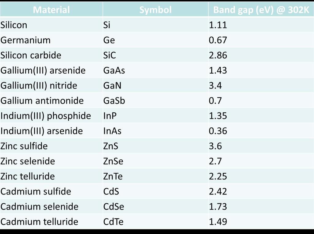
15 Compound Semiconductors Made out of elements from different columns of the periodic table III-V, II-VI, IV-VI, or IV-IV III-V is the most used compound GaAs and InP Same average number of valence electrons per silicon atom Column represent the number of valence electrons
16 Abbreviated Periodic Table
17 Indium Antimonide (InSb) the 1 st III-V Discovered in 1950 Easily synthesized Electron Mobility Low bandgap energy (E g =0.17 ev) Good for infrared detection
18 Other important III-V compounds Semiconductor Photodetectors GaAs Bandgap of E g = 1.43 ev Direct bandgap InP Bandgap of E g = 1.35 ev Direct bandgap GaP Bandgap of Eg = 2.1 ev Indirect bandgap
19 Elemental Versus III-V III-V has a higher mobilities and higher velocities III-V are more efficient High-Speed optoelectronic devices Higher Responsivity Many III-Vs are direct bandgap
20
21 Direct vs. Indirect Bandgap Semiconductors
, since photon momentum is very small.")
22 Absorption Coefficient Direct bandgap semiconductors (GaAs, InAs, InP, GaSb, InGaAs, GaAsSb), the photon absorption does not require assistant from lattice vibrations. The photon is absorbed and the electron is excited directly from the VB to CB without a change in its k-vector (crystal momentum ħk), since photon momentum is very small. k k CB VB = photon momentum 0 Absorption coefficient α for direct bandgap semiconductors rise sharply with decreasing wavelength from λ g (GaAs and InP).

23 Absorption Coefficient Indirect bandgap semiconductors (Si and Ge), the photon absorption requires assistant from lattice vibrations (phonon). If K is wave vector of lattice wave, then ħk represents the momentum associated with lattice vibration ħk is phonon momentum. k k = phonon momentum = CB VB K Thus, the probability of photon absorption is not as high as in a direct transition.
24 Absorption Coefficient Photon absorption in a direct bandgap semiconductor: E ph =hv>e g E Photon absorption in an indirect bandgap semiconductor: E ph =hv>e g ± E phonon E C B E C Direct Bandgap E g E V Photon Photon C B Indirect Bandgap E C E g V B V B E V Phonons k k k k
25 Quantum Efficiency and Responsivity Quantum efficiency, η, is the number of carriers (EHP) collected to produce the photocurrent, I ph, divided by the number of incident photons (where P inc is incident optical power): I ph / e I ph hv η = = * Pinc / hv e Pinc η depends on absorption coefficient and thickness of absorbing region. Responsivity of a detector, R, is a performance parameter that indicates the magnitude of the electrical signal output from a photodetector in response to a particular light power: R = I ph /P inc = (ηe)/hν = (ηλ)/1.24 (µm)
26 Photodiodes Energy Level Diagram for V = 0 (zero bias) p n Electron Energy Conduction Band Hole E g Valence Band Energy
27 SEMICONDUCTOR JUNCTION PHOTODIODE Reverse Biased Photodiode p n hf Electron Energy hf E E g Junction Region
28 SEMICONDUCTOR JUNCTION PHOTODIODE An incident photon absorbed in the junction gives up its energy, creating a free electron and a free hole in the junction. The generated free charges move due to the strong electric field E in the junction. Recall that the electric field is generated by the change in electric potential V given by: E = V
29 SEMICONDUCTOR JUNCTION As before PHOTODIODE A condition for detection is that the photon energy be greater than the bandgap energy: hf E g f E h g λ c = hc E g λ c = 1.24 E g Example: Compute the cutoff wavelength for Silicon. The bandgap energy for silicon is E g = 1.1 ev 1.24 λ c = = 1. 1µ m 1.1
30 Light Transmission
31 SEMICONDUCTOR JUNCTION PHOTODIODE Response Time The pn photodiode responds slowly because many photons are absorbed in the n and p regions close to the junction. hf Diffusion p - E n Electron Energy +
32 SEMICONDUCTOR JUNCTION PHOTODIODE The free charge carriers diffuse slowly (gold arrow) into the junction where they are accelerated (green arrow) by the large electric field there. This produces a delayed current in the external circuit, causing pulse spreading, lowering the data rates that can be received, and reducing the analog 3-dB frequency bandwidth of the receiver.
33 SEMICONDUCTOR JUNCTION PHOTODIODE The analog 3-dB frequency bandwidth is typically about t r = 1 µs for pn junction photodetectors. f = = = = t 10 3 db 6 r khz The solution to this problem is the pin diode.
34 PIN Photodiode PIN Photodiode hf Intrinsic Layer i p - + E n V - Thin Layer R L v +
35 PIN PHOTODIODE Materials Material Wavelength Range (µm) Peak Response λ (µm) Peak Responsivity ρ (A/W) Silicon Germanium InGaAs
36 PIN PHOTODIODE The intrinsic layer is on an insulator. Most of the photons are absorbed in that layer because it is long. Most of the voltage drop is across the intrinsic layer. This creates a high electric field in the intrinsic layer. Now there is no delay caused by diffusion and the response time is much faster that that of a pn photodiode. t tr t tr = 1 2 = τ ( modulation period) RC
37 Photoresponse Bandwidth Tradeoff The advantage of a PIN photodiode is that it has a controlled depletion region or width, which can be tailored to meet the requirements of photoresponse and bandwidth. By increasing the thickness of the intrinsic region, the photoresponse can be enhanced. However, increasing the thickness of the active region reduces the bandwidth. This photoresponse-bandwidth tradeoff limits the amount of tailoring that can be done.
38 Speed of Response Transit time: Time for free charges to move across the depletion region (the intrinsic layer in a pin photodiode). The speed of response is ultimately limited by the transit time. Example: d = depletion width = 50 µm v = carrier velocity = 5 x 10 4 m/s Then the transit time is: d v t = = 9 = 10 s = 1ns 4
39 Speed of Response The detector s rise time is on the order of its transit time. The bandwidth is limited to: f = 3 db 0.35 In addition to the transit time, the detector s capacitance and load resistance also limit the response speed. t r
40 Speed of Response Detector Equivalent Circuit i d (ρp) C d R L v C d : Diode Capacitance The rise time of this circuit is: t = 2.19RC r L D
41 Speed of Response The 3-dB bandwidth is f db = = = tr 2.19RLCd 1 2π R C L d This establishes the relationship between the load resistance and the bandwidth. The larger the load resistance, the smaller the bandwidth.

42 Metal Semiconductor Metal PD V d1 V d2 g The energy band diagram for an MSM PD in thermal equilibrium is shown above, where the electron Schottky barrier heights and built in voltages are labeled Φ n1 and Φ n2, V d1 and V d2, respectively. Φ p2 is the hole Schottky barrier height from the second contact, and g is the gap length between the contacts.
 MSM: By inverting, low capacitance per unit area is maintained and responsivity is dramatically improved because the fingers are on")
43 43 Conventional Versus Inverted MSM Photodetectors MSM Advantage: Low capacitance per unit area compared to typical PIN PDs MSM Disadvantage: Shadowing by interdigitated electrodes reduces responsivity Inverted (I-) MSM: By inverting, low capacitance per unit area is maintained and responsivity is dramatically improved because the fingers are on the bottom
 I-MSM")
44 Thin Film I-MSM Photodetector Silicon host substrate GaAs thin film (1 µm thick) I-MSM PD 44
45 Metal-Semiconductor-Metal Photodetector (MSM PD) and LED Device Structure MSM PD material Undoped GaAs (1000 nm) AlAs (200 nm) GaAs (Substrate) LED Material GaAs (20 nm) GaAlAs (1000 nm) GaAs (1000 nm) GaAlAs (1000 nm) GaAs (20 nm) AlAs (200 nm) GaAs (50 nm) GaAs (Substrate) Each device is grown separately An AlAs sacrificial etch layer is included in the growth Different structures can be used to optimize the performance of each individual device 45


46 How the I-MSM Works Incident photons Electric field line EHP #3 Lines of equipotential EHP #2 0 V EHP #1 +5 V 46
47 Frequency Response
48 Current-Voltage Characteristic I D is called the dark current. This is the current that flows when no photons are incident (this is just the diode reverse leakage current). It is due to thermal generation of minority charge carriers. Small optical signals are masked by the dark current. For good signal reception, the received power must greatly exceed levels of power which generate currents on the order of the dark current. 48
49 Current-Voltage Characteristic Typical Dark Current Values Silicon InGaAs Germanium 2 na 50 na 500 na Example: Compute the responsivity from the v d i d curve given several slides back. Solution: i d = -10 µa when P = 20 µw, so that i d 10 ρ = = = 0.5 µ A/ µ W P 20
50 Current-Voltage Characteristic Example: Let I D = 2 na in the previous example. What is the minimum detectable optical power if we can detect a signal current equal to (or greater than) the dark current? Solution: We want i = 2 na as a minimum. i = ρ P i 2nA P = = = 4nW ρ 0.5nA / nw We can detect powers as low as 4 nw.
51 Noise and Detection
52 Noise degrades signals. Without noise, it would not matter how little optical power arrived at the receiver. Signal quality is measured in several ways. Analog systems: The signal-to-noise ratio (SNR) is the measure. Digital systems: The bit-error-rate (BER) is the measure.
53 Thermal and Shot Noise
54 Thermal Noise Recall the simple receiver circuit : P V b - + i R L v
55 Even if P = 0 (and the photodiode dark current is zero), a current i = i NT will exist in resistor R L. It has zero average value, but it is random, like: i NT t
56 The current arises from the random thermal motion of the electrons. The instantaneous noise power is R L i 2 NT The average thermal noise power is R L i 2 NT R L i 2 NT R L i 2 NT t
57 i 2 NT = mean square thermal noise current. It is given by : i 2 NT = 4kT f /R L k = 1.38 x J /K, Boltzmann constant T = temperature, K f = receiver s bandwidth. Usually f is a bit larger than the information bandwidth.
58 The load resistor s equivalent circuit looks like: i 2 NT = 4kT f /R L R L v where R L is an ideal (noiseless) resistor.
59 Shot Noise It is caused by the discrete nature of charge carriers (electrons and holes). Consider the single emitted photoelectron, shown for vacuum phototube. Cathode hf electron Anode V b i R L
60 A current exists in the circuit during the transit time (τ) of the emitted electron. τ = time for travel from cathode to anode. The electron recombines at the anode with a positive ion. The current caused by a single electron looks something like : h(t) t τ
61 Every electron produces the same current pulse shape. Consider constant optical power P incident on the detector. The expected current is : i i = (ηe / hf)p t This current is made up of numerous pulses of the type shown by h(t).
62 Example : t The pulses start at random times, t N. The total current is the sum of these pulses. i = Σ N h(t - t N )
63 Total current: i (ηe /hf)p t The average current is still: i = (ηe /hf)p but noise is superimposed onto this current. This is shot noise.
64 The shot noise current is: i NS = Σ N h(t - t N ) - (ηe /hf)p i 2 NS = 2eI f f = receiver s bandwidth I = average current. I = i S + I D where i S I D = average of the signal current = average dark current
65 The equivalent circuit for shot noise is just a noise current generator, as shown below. i 2 NS = 2eI f
66 Signal-to-Noise Ratio
67 Consider the equivalent circuit of a photodiode receiver. R s i S C d R d v C d = diode s junction capacitance (small) R d = diode s junction resistance (large) R s = diode s bulk series (n and p) resistance (small)
68 i S is the photocurrent. As before, it is given by i s = (ηep/hf) = ρp For simplicity, assume R s = 0 and R d = infinite. Also neglect C d for purposes of noise calculations, since it does not affect the noise in the circuit. The simplified receiving circuit, including all sources of thermal and shot noise is now:
69 i S i 2 NT i 2 NS R L We will use this circuit to compute SNR.
70 Constant Power SNR Let the incident optical power P be a constant. This corresponds to a binary 1 in a digital system. Compute the SNR. SNR = average signal power / average noise power These are the electrical powers. From the equivalent circuit, we see that SNR = (R L i 2 S) / (R L i 2 NS + R L i 2 NT) SNR = P ES / (P NS + P NT ) SNR = i 2 S / ( i 2 NS + i 2 NT)
71 These equations are general. For the special case where P = a constant: i S = i S = (ηe / hf)p = ρp P ES = R L i 2 S = (ηe P/ hf) 2 R L P NT = R L i 2 NT = (4kT f / R L ) R L = 4kT f P NS = R L i 2 NS = 2e[ I D + (ηe P/ hf)] f R L Then SNR = [(ηe P/ hf) 2 R L ] {2e[ I D + (ηe P/ hf)] f R L }+ 4kT f
72 Example: Light source is an LED, 10 mw output power, λ = 0.85 µm. The system losses are: coupling loss = 14 db fiber loss = 20 db connector losses = 10 db Total loss = 44 db
73 Compute the received power. db = log (P R /P T ) - 44 = log (P R /P T ) (P R / P T ) = P R = 10 x = 10(3.98 x 10⁻⁵ ) P R = 4 x 10⁻⁴ mw Alternative calculation for the received power: P T = 10 mw = 10 dbm Loss = - 44 db P R = - 34 dbm
74 Check : dbm = 10 log P R -34 = 10 log P R P R = = 4 x 10⁻⁴ mw This result checks. The receiver has the following characteristics: ρ = 0.5 A/W (responsivity) I D = 2 na (dark current) R L = 50 Ω (load resistance)
75 f = 10 MHz (receiver bandwidth) T = 300 K (27 0 C) receiver temperature Find : Signal current and power Shot noise power Thermal noise power SNR
76 Solution : Signal Current i S = ρp R = 0.5(4 x 10⁻⁴ ) = 2 x 10⁻⁴ ma i S = 0.2 µa = 200 na i S = 200 na >> I D = 2 na Signal Power P ES = R L i 2 S = 50(0.2 x 10⁻⁶ ) 2 = 2 x W Shot Noise Power P NS = 2e i S R L f = 2(1.6 x ) (0.2 x 10⁻⁶ ) (50)10 7 P NS = 3.2 x W
77 Thermal Noise Power P NT = 4kT f = 4(1.38 x ) 300 x 10 7 P NT = 1.66 x W Note P NT >> P NS Thus, we have a thermal-noise limited system, and SNR = P ES / P NT = 2 x /1.66 x = 12 SNR db = 10 log SNR SNR db = 10 log 12 = 10.8 db
78 If the system were shot-noise limited, then SNR = ηp /2hf f = i s /2e f SNR = 0.2 x 10⁻⁶ / 2(1.6 x ) 10 7 = 62,500 SNR db = 10 log 62,500 = 48 db Note the improvement if the system were shot-noise limited. We can approach this higher SNR if we use a photodetector with internal gain, or use heterodyne detection.
79 References 1. Joseph Palais. Fiber Optics Communications, 5 th Edition. New Jersey: Prentice Hall, Frank L. Pedrotti and Leno Pedrotti. Introduction to Optics. New Jersey: Prentice Hall, Pallab Bhattacharya. Semiconductor Optoelectronic Devices, 2 nd Edition. New Jersey: Prentice Hall, 1997.
LEC E T C U T R U E R E 17 -Photodetectors
 LECTURE 17 -Photodetectors Topics to be covered Photodetectors PIN photodiode Avalanche Photodiode Photodetectors Principle of the p-n junction Photodiode A generic photodiode. Photodetectors Principle
Chapter 4. Photodetectors
 Chapter 4 Photodetectors Types of photodetectors: Photoconductos Photovoltaic Photodiodes Avalanche photodiodes (APDs) Resonant-cavity photodiodes MSM detectors In telecom we mainly use PINs and APDs.
OPTI510R: Photonics. Khanh Kieu College of Optical Sciences, University of Arizona Meinel building R.626
 OPTI510R: Photonics Khanh Kieu College of Optical Sciences, University of Arizona kkieu@optics.arizona.edu Meinel building R.626 Announcements Homework #6 is assigned, due May 1 st Final exam May 8, 10:30-12:30pm
Photosynthesis & Solar Power Harvesting
 Lecture 23 Semiconductor Detectors - Photodetectors Principle of the pn junction photodiode Absorption coefficient and photodiode materials Properties of semiconductor detectors The pin photodiodes Avalanche
Lect. 10: Photodetectors
 Photodetection: Absorption => Current Generation h Currents Materials for photodetection: E g < h Various methods for generating currents with photo-generated carriers: photoconductors, photodiodes, avalanche
Lecture 12. Semiconductor Detectors - Photodetectors
 Lecture 12 Semiconductor Detectors - Photodetectors Principle of the pn junction photodiode Absorption coefficient and photodiode materials Properties of semiconductor detectors The pin photodiodes Avalanche
Single Photon detectors
 Single Photon detectors Outline Motivation for single photon detection Semiconductor; general knowledge and important background Photon detectors: internal and external photoeffect Properties of semiconductor
Photodetector Basics
 Photodetection: Absorption => Current Generation hυ Currents Materials for photodetection: t ti E g
Electron Energy, E E = 0. Free electron. 3s Band 2p Band Overlapping energy bands. 3p 3s 2p 2s. 2s Band. Electrons. 1s ATOM SOLID.
 Electron Energy, E Free electron Vacuum level 3p 3s 2p 2s 2s Band 3s Band 2p Band Overlapping energy bands Electrons E = 0 1s ATOM 1s SOLID In a metal the various energy bands overlap to give a single
Course overview. Me: Dr Luke Wilson. The course: Physics and applications of semiconductors. Office: E17 open door policy
 Course overview Me: Dr Luke Wilson Office: E17 open door policy email: luke.wilson@sheffield.ac.uk The course: Physics and applications of semiconductors 10 lectures aim is to allow time for at least one
Chemistry Instrumental Analysis Lecture 8. Chem 4631
 Chemistry 4631 Instrumental Analysis Lecture 8 UV to IR Components of Optical Basic components of spectroscopic instruments: stable source of radiant energy transparent container to hold sample device
Photodetectors Read: Kasip, Chapter 5 Yariv, Chapter 11 Class Handout. ECE 162C Lecture #13 Prof. John Bowers
 Photodetectors Read: Kasip, Chapter 5 Yariv, Chapter 11 Class Handout ECE 162C Lecture #13 Prof. John Bowers Definitions Quantum efficiency η: Ratio of the number of electrons collected to the number of
Photodetector. Prof. Woo-Young Choi. Silicon Photonics (2012/2) Photodetection: Absorption => Current Generation. Currents
 Photodetection: Absorption => Current Generation. Currents") Photodetection: Absorption => Current Generation h Currents Materials for photodetection: E g < h Various methods for generating currents with photo-generated carriers: photoconductors, photodiodes, avalanche
Photodetection: Absorption => Current Generation h Currents Materials for photodetection: E g < h Various methods for generating currents with photo-generated carriers: photoconductors, photodiodes, avalanche
ECEN 5645 Introduc0on to Optoelectronics Class Mee0ng 25. Non- PIN Solid State Detectors
 ECEN 5645 Introduc0on to Optoelectronics Class Mee0ng 25 Non- PIN Solid State Detectors Today s Topics Avalanche Photodiodes Problem 5.6 APD Numerics and Examples Heterojunc0on Detectors Problem 5.10 Quantum
EE 5344 Introduction to MEMS CHAPTER 5 Radiation Sensors
 EE 5344 Introduction to MEMS CHAPTER 5 Radiation Sensors 5. Radiation Microsensors Radiation µ-sensors convert incident radiant signals into standard electrical out put signals. Radiant Signals Classification
ELECTRONIC DEVICES AND CIRCUITS SUMMARY
 ELECTRONIC DEVICES AND CIRCUITS SUMMARY Classification of Materials: Insulator: An insulator is a material that offers a very low level (or negligible) of conductivity when voltage is applied. Eg: Paper,
Chapter 1 Overview of Semiconductor Materials and Physics
 Chapter 1 Overview of Semiconductor Materials and Physics Professor Paul K. Chu Conductivity / Resistivity of Insulators, Semiconductors, and Conductors Semiconductor Elements Period II III IV V VI 2 B
Chapter 7. Solar Cell
 Chapter 7 Solar Cell 7.0 Introduction Solar cells are useful for both space and terrestrial application. Solar cells furnish the long duration power supply for satellites. It converts sunlight directly
Chapter 17. λ 2 = 1.24 = 6200 Å. λ 2 cutoff at too short a wavelength λ 1 cutoff at to long a wavelength (increases bandwidth for noise reduces S/N).
.") 70 Chapter 17 17.1 We wish to use a photodiode as a detector for a signal of 9000 Å wavelength. Which would be the best choice of material for the photodiode, a semiconductor of bandgap = 0.5 ev, bandgap
70 Chapter 17 17.1 We wish to use a photodiode as a detector for a signal of 9000 Å wavelength. Which would be the best choice of material for the photodiode, a semiconductor of bandgap = 0.5 ev, bandgap
1 Name: Student number: DEPARTMENT OF PHYSICS AND PHYSICAL OCEANOGRAPHY MEMORIAL UNIVERSITY OF NEWFOUNDLAND. Fall :00-11:00
 1 Name: DEPARTMENT OF PHYSICS AND PHYSICAL OCEANOGRAPHY MEMORIAL UNIVERSITY OF NEWFOUNDLAND Final Exam Physics 3000 December 11, 2012 Fall 2012 9:00-11:00 INSTRUCTIONS: 1. Answer all seven (7) questions.
Purpose: To convert the received optical signal into an electrical lsignal.
 OPTICAL DETECTORS Optical Detectors Purpose: To convert the received optical signal into an electrical lsignal. Requirements For Detector HIGH SENSITIVITY (at operating wave lengths) at normal op. temp
Lecture 2. Introduction to semiconductors Structures and characteristics in semiconductors
 Lecture 2 Introduction to semiconductors Structures and characteristics in semiconductors Semiconductor p-n junction Metal Oxide Silicon structure Semiconductor contact Literature Glen F. Knoll, Radiation
Lecture 2. Introduction to semiconductors Structures and characteristics in semiconductors
 Lecture 2 Introduction to semiconductors Structures and characteristics in semiconductors Semiconductor p-n junction Metal Oxide Silicon structure Semiconductor contact Literature Glen F. Knoll, Radiation
EE 6313 Homework Assignments
 EE 6313 Homework Assignments 1. Homework I: Chapter 1: 1.2, 1.5, 1.7, 1.10, 1.12 [Lattice constant only] (Due Sept. 1, 2009). 2. Homework II: Chapter 1, 2: 1.17, 2.1 (a, c) (k = π/a at zone edge), 2.3
FIBER OPTICS. Prof. R.K. Shevgaonkar. Department of Electrical Engineering. Indian Institute of Technology, Bombay. Lecture: 14.
 FIBER OPTICS Prof. R.K. Shevgaonkar Department of Electrical Engineering Indian Institute of Technology, Bombay Lecture: 14 Optical Sources Fiber Optics, Prof. R.K. Shevgaonkar, Dept. of Electrical Engineering,
Photodiodes and other semiconductor devices
 Photodiodes and other semiconductor devices Chem 243 Winter 2017 What is a semiconductor? no e - Empty e levels Conduction Band a few e - Empty e levels Filled e levels Filled e levels lots of e - Empty
ET3034TUx Utilization of band gap energy
 ET3034TUx - 3.3.1 - Utilization of band gap energy In the last two weeks we have discussed the working principle of a solar cell and the external parameters that define the performance of a solar cell.
Sample Exam # 2 ECEN 3320 Fall 2013 Semiconductor Devices October 28, 2013 Due November 4, 2013
 Sample Exam # 2 ECEN 3320 Fall 203 Semiconductor Devices October 28, 203 Due November 4, 203. Below is the capacitance-voltage curve measured from a Schottky contact made on GaAs at T 300 K. Figure : Capacitance
Chapter 3 The InAs-Based nbn Photodetector and Dark Current
 68 Chapter 3 The InAs-Based nbn Photodetector and Dark Current The InAs-based nbn photodetector, which possesses a design that suppresses surface leakage current, is compared with both a commercially available
Outline. Photosensors in biology and in semiconductors. The visual pathway Bottom view. The visual pathway Side view
 Outline Photosensors in biology and in semiconductors CNS WS07-08 Class 1 Photosensors in biology The visual pathway and the retina Photoreceptors and the fovea Giacomo Indiveri Institute of Neuroinformatics
Semiconductor Detectors
 Semiconductor Detectors Summary of Last Lecture Band structure in Solids: Conduction band Conduction band thermal conductivity: E g > 5 ev Valence band Insulator Charge carrier in conductor: e - Charge
Designing Information Devices and Systems II A. Sahai, J. Roychowdhury, K. Pister Discussion 1A
 EECS 16B Spring 2019 Designing Information Devices and Systems II A. Sahai, J. Roychowdhury, K. Pister Discussion 1A 1 Semiconductor Physics Generally, semiconductors are crystalline solids bonded into
Classification of Solids
 Classification of Solids Classification by conductivity, which is related to the band structure: (Filled bands are shown dark; D(E) = Density of states) Class Electron Density Density of States D(E) Examples
Practical 1P4 Energy Levels and Band Gaps
 Practical 1P4 Energy Levels and Band Gaps What you should learn from this practical Science This practical illustrates some of the points from the lecture course on Elementary Quantum Mechanics and Bonding
PHOTOVOLTAICS Fundamentals
 PHOTOVOLTAICS Fundamentals PV FUNDAMENTALS Semiconductor basics pn junction Solar cell operation Design of silicon solar cell SEMICONDUCTOR BASICS Allowed energy bands Valence and conduction band Fermi
Engineering 2000 Chapter 8 Semiconductors. ENG2000: R.I. Hornsey Semi: 1
 Engineering 2000 Chapter 8 Semiconductors ENG2000: R.I. Hornsey Semi: 1 Overview We need to know the electrical properties of Si To do this, we must also draw on some of the physical properties and we
Photodetectors and their Spectral Ranges
 Photodetectors and their Spectral Ranges SINGLE ELEMENT IMAGE - photoemission devices vacuum photodiode pickup tubes (or external gas photodiode image intensifiers photoelectric devices) photomultiplier
Lecture 15: Optoelectronic devices: Introduction
 Lecture 15: Optoelectronic devices: Introduction Contents 1 Optical absorption 1 1.1 Absorption coefficient....................... 2 2 Optical recombination 5 3 Recombination and carrier lifetime 6 3.1
R. Ludwig and G. Bogdanov RF Circuit Design: Theory and Applications 2 nd edition. Figures for Chapter 6
 R. Ludwig and G. Bogdanov RF Circuit Design: Theory and Applications 2 nd edition Figures for Chapter 6 Free electron Conduction band Hole W g W C Forbidden Band or Bandgap W V Electron energy Hole Valence
Fall 2014 Nobby Kobayashi (Based on the notes by E.D.H Green and E.L Allen, SJSU) 1.0 Learning Objectives
 1.0 Learning Objectives") University of California at Santa Cruz Electrical Engineering Department EE-145L: Properties of Materials Laboratory Lab 7: Optical Absorption, Photoluminescence Fall 2014 Nobby Kobayashi (Based on the
University of California at Santa Cruz Electrical Engineering Department EE-145L: Properties of Materials Laboratory Lab 7: Optical Absorption, Photoluminescence Fall 2014 Nobby Kobayashi (Based on the
Laser Basics. What happens when light (or photon) interact with a matter? Assume photon energy is compatible with energy transition levels.
 interact with a matter? Assume photon energy is compatible with energy transition levels.") What happens when light (or photon) interact with a matter? Assume photon energy is compatible with energy transition levels. Electron energy levels in an hydrogen atom n=5 n=4 - + n=3 n=2 13.6 = [ev]
What happens when light (or photon) interact with a matter? Assume photon energy is compatible with energy transition levels. Electron energy levels in an hydrogen atom n=5 n=4 - + n=3 n=2 13.6 = [ev]
Advantages / Disadvantages of semiconductor detectors
 Advantages / Disadvantages of semiconductor detectors Semiconductor detectors have a high density (compared to gas detector) large energy loss in a short distance diffusion effect is smaller than in gas
3.1 Introduction to Semiconductors. Y. Baghzouz ECE Department UNLV
 3.1 Introduction to Semiconductors Y. Baghzouz ECE Department UNLV Introduction In this lecture, we will cover the basic aspects of semiconductor materials, and the physical mechanisms which are at the
Practical 1P4 Energy Levels and Band Gaps
 Practical 1P4 Energy Levels and Band Gaps What you should learn from this practical Science This practical illustrates some of the points from the lecture course on Elementary Quantum Mechanics and Bonding
Metal Vapour Lasers Use vapoured metal as a gain medium Developed by W. Silfvast (1966) Two types: Ionized Metal vapour (He-Cd) Neutral Metal vapour
 Two types: Ionized Metal vapour (He-Cd) Neutral Metal vapour") Metal Vapour Lasers Use vapoured metal as a gain medium Developed by W. Silfvast (1966) Two types: Ionized Metal vapour (He-Cd) Neutral Metal vapour (Cu) All operate by vaporizing metal in container Helium
Metal Vapour Lasers Use vapoured metal as a gain medium Developed by W. Silfvast (1966) Two types: Ionized Metal vapour (He-Cd) Neutral Metal vapour (Cu) All operate by vaporizing metal in container Helium
Comunicações Ópticas Noise in photodetectors MIEEC EEC038. Henrique Salgado Receiver operation
 Comunicações Ópticas Noise in photodetectors 2007-2008 MIEEC EEC038 Henrique Salgado hsalgado@fe.up.pt Receiver operation Noise plays a fundamental role in design of an optical receiver Optical data link
KATIHAL FİZİĞİ MNT-510
 KATIHAL FİZİĞİ MNT-510 YARIİLETKENLER Kaynaklar: Katıhal Fiziği, Prof. Dr. Mustafa Dikici, Seçkin Yayıncılık Katıhal Fiziği, Şakir Aydoğan, Nobel Yayıncılık, Physics for Computer Science Students: With
Introduction to Semiconductor Physics. Prof.P. Ravindran, Department of Physics, Central University of Tamil Nadu, India
 Introduction to Semiconductor Physics 1 Prof.P. Ravindran, Department of Physics, Central University of Tamil Nadu, India http://folk.uio.no/ravi/cmp2013 Review of Semiconductor Physics Semiconductor fundamentals
Chapter 4 Scintillation Detectors
 Med Phys 4RA3, 4RB3/6R03 Radioisotopes and Radiation Methodology 4-1 4.1. Basic principle of the scintillator Chapter 4 Scintillation Detectors Scintillator Light sensor Ionizing radiation Light (visible,
SEMICONDUCTOR PHYSICS REVIEW BONDS,
 SEMICONDUCTOR PHYSICS REVIEW BONDS, BANDS, EFFECTIVE MASS, DRIFT, DIFFUSION, GENERATION, RECOMBINATION February 3, 2011 The University of Toledo, Department of Physics and Astronomy SSARE, PVIC Principles
Chap. 11 Semiconductor Diodes
 Chap. 11 Semiconductor Diodes Semiconductor diodes provide the best resolution for energy measurements, silicon based devices are generally used for charged-particles, germanium for photons. Scintillators
COURSE OUTLINE. Introduction Signals and Noise Filtering Sensors: PD5 Avalanche PhotoDiodes. Sensors, Signals and Noise 1
 Sensors, Signals and Noise 1 COURSE OUTLINE Introduction Signals and Noise Filtering Sensors: PD5 Avalanche PhotoDiodes Avalanche Photo-Diodes (APD) 2 Impact ionization in semiconductors Linear amplification
Phys 4061 Lecture Thirteen Photodetectors
 Phys 4061 Lecture Thirteen Photodetectors Recall properties of indirect band gap materials that are used as photodetectors Photoelectric Effect in Semiconductors hν > Eg + χ χ is the electron affinity
SEMICONDUCTOR PHYSICS
 SEMICONDUCTOR PHYSICS by Dibyendu Chowdhury Semiconductors The materials whose electrical conductivity lies between those of conductors and insulators, are known as semiconductors. Silicon Germanium Cadmium
Semiconductor Physics Problems 2015
 Semiconductor Physics Problems 2015 Page and figure numbers refer to Semiconductor Devices Physics and Technology, 3rd edition, by SM Sze and M-K Lee 1. The purest semiconductor crystals it is possible
Schottky Rectifiers Zheng Yang (ERF 3017,
 ECE442 Power Semiconductor Devices and Integrated Circuits Schottky Rectifiers Zheng Yang (ERF 3017, email: yangzhen@uic.edu) Power Schottky Rectifier Structure 2 Metal-Semiconductor Contact The work function
Atmospheric Extinction
 Atmospheric Extinction Calibrating stellar photometry requires correction for loss of light passing through the atmosphere. Atmospheric Rayleigh and aerosol scattering preferentially redirects blue light
ELEC 4700 Assignment #2
 ELEC 4700 Assignment #2 Question 1 (Kasop 4.2) Molecular Orbitals and Atomic Orbitals Consider a linear chain of four identical atoms representing a hypothetical molecule. Suppose that each atomic wavefunction
Lecture 2. Semiconductor Physics. Sunday 4/10/2015 Semiconductor Physics 1-1
 Lecture 2 Semiconductor Physics Sunday 4/10/2015 Semiconductor Physics 1-1 Outline Intrinsic bond model: electrons and holes Charge carrier generation and recombination Intrinsic semiconductor Doping:
16EC401 BASIC ELECTRONIC DEVICES UNIT I PN JUNCTION DIODE. Energy Band Diagram of Conductor, Insulator and Semiconductor:
 16EC401 BASIC ELECTRONIC DEVICES UNIT I PN JUNCTION DIODE Energy bands in Intrinsic and Extrinsic silicon: Energy Band Diagram of Conductor, Insulator and Semiconductor: 1 2 Carrier transport: Any motion
Unit IV Semiconductors Engineering Physics
 Introduction A semiconductor is a material that has a resistivity lies between that of a conductor and an insulator. The conductivity of a semiconductor material can be varied under an external electrical
CME 300 Properties of Materials. ANSWERS: Homework 9 November 26, As atoms approach each other in the solid state the quantized energy states:
 CME 300 Properties of Materials ANSWERS: Homework 9 November 26, 2011 As atoms approach each other in the solid state the quantized energy states: are split. This splitting is associated with the wave
Lecture 8. Equations of State, Equilibrium and Einstein Relationships and Generation/Recombination
 Lecture 8 Equations of State, Equilibrium and Einstein Relationships and Generation/Recombination Reading: (Cont d) Notes and Anderson 2 sections 3.4-3.11 Energy Equilibrium Concept Consider a non-uniformly
Bohr s Model, Energy Bands, Electrons and Holes
 Dual Character of Material Particles Experimental physics before 1900 demonstrated that most of the physical phenomena can be explained by Newton's equation of motion of material particles or bodies and
Energetic particles and their detection in situ (particle detectors) Part II. George Gloeckler
 Part II. George Gloeckler") Energetic particles and their detection in situ (particle detectors) Part II George Gloeckler University of Michigan, Ann Arbor, MI University of Maryland, College Park, MD Simple particle detectors Gas-filled
Energetic particles and their detection in situ (particle detectors) Part II George Gloeckler University of Michigan, Ann Arbor, MI University of Maryland, College Park, MD Simple particle detectors Gas-filled
EECS130 Integrated Circuit Devices
 EECS130 Integrated Circuit Devices Professor Ali Javey 8/30/2007 Semiconductor Fundamentals Lecture 2 Read: Chapters 1 and 2 Last Lecture: Energy Band Diagram Conduction band E c E g Band gap E v Valence
Semiconductors and Optoelectronics. Today Semiconductors Acoustics. Tomorrow Come to CH325 Exercises Tours
 Semiconductors and Optoelectronics Advanced Physics Lab, PHYS 3600 Don Heiman, Northeastern University, 2017 Today Semiconductors Acoustics Tomorrow Come to CH325 Exercises Tours Semiconductors and Optoelectronics
Chapter 3 Properties of Nanostructures
 Chapter 3 Properties of Nanostructures In Chapter 2, the reduction of the extent of a solid in one or more dimensions was shown to lead to a dramatic alteration of the overall behavior of the solids. Generally,
Chapter 5. Semiconductor Laser
 Chapter 5 Semiconductor Laser 5.0 Introduction Laser is an acronym for light amplification by stimulated emission of radiation. Albert Einstein in 1917 showed that the process of stimulated emission must
Solid State Device Fundamentals
 4. lectrons and Holes Solid State Device Fundamentals NS 45 Lecture Course by Alexander M. Zaitsev alexander.zaitsev@csi.cuny.edu Tel: 718 982 2812 4N101b 1 4. lectrons and Holes Free electrons and holes
Comparison of Ge, InGaAs p-n junction solar cell
 ournal of Physics: Conference Series PAPER OPEN ACCESS Comparison of Ge, InGaAs p-n junction solar cell To cite this article: M. Korun and T. S. Navruz 16. Phys.: Conf. Ser. 77 135 View the article online
Silicon Detectors in High Energy Physics
 Thomas Bergauer (HEPHY Vienna) IPM Teheran 22 May 2011 Sunday: Schedule Silicon Detectors in Semiconductor Basics (45 ) Detector concepts: Pixels and Strips (45 ) Coffee Break Strip Detector Performance
EE 5611 Introduction to Microelectronic Technologies Fall Tuesday, September 23, 2014 Lecture 07
 EE 5611 Introduction to Microelectronic Technologies Fall 2014 Tuesday, September 23, 2014 Lecture 07 1 Introduction to Solar Cells Topics to be covered: Solar cells and sun light Review on semiconductor
Junction Diodes. Tim Sumner, Imperial College, Rm: 1009, x /18/2006
 Junction Diodes Most elementary solid state junction electronic devices. They conduct in one direction (almost correct). Useful when one converts from AC to DC (rectifier). But today diodes have a wide
MSE 310/ECE 340: Electrical Properties of Materials Fall 2014 Department of Materials Science and Engineering Boise State University
 MSE 310/ECE 340: Electrical Properties of Materials Fall 2014 Department of Materials Science and Engineering Boise State University Practice Final Exam 1 Read the questions carefully Label all figures
Section 12: Intro to Devices
 Section 12: Intro to Devices Extensive reading materials on reserve, including Robert F. Pierret, Semiconductor Device Fundamentals EE143 Ali Javey Bond Model of Electrons and Holes Si Si Si Si Si Si Si
1 Review of semiconductor materials and physics
 Part One Devices 1 Review of semiconductor materials and physics 1.1 Executive summary Semiconductor devices are fabricated using specific materials that offer the desired physical properties. There are
Lecture 2. Introduction to semiconductors Structures and characteristics in semiconductors. Fabrication of semiconductor sensor
 Lecture 2 Introduction to semiconductors Structures and characteristics in semiconductors Semiconductor p-n junction Metal Oxide Silicon structure Semiconductor contact Fabrication of semiconductor sensor
Sensor Technology. Summer School: Advanced Microsystems Technologies for Sensor Applications
 Sensor Technology Summer School: Universidade Federal do Rio Grande do Sul (UFRGS) Porto Alegre, Brazil July 12 th 31 st, 2009 1 Outline of the Lecture: Philosophy of Sensing Instrumentation and Systems
EE301 Electronics I , Fall
 EE301 Electronics I 2018-2019, Fall 1. Introduction to Microelectronics (1 Week/3 Hrs.) Introduction, Historical Background, Basic Consepts 2. Rewiev of Semiconductors (1 Week/3 Hrs.) Semiconductor materials
Electrons are shared in covalent bonds between atoms of Si. A bound electron has the lowest energy state.
 Photovoltaics Basic Steps the generation of light-generated carriers; the collection of the light-generated carriers to generate a current; the generation of a large voltage across the solar cell; and
Physics of Semiconductor Devices. Unit 2: Revision of Semiconductor Band Theory
 Physics of Semiconductor Devices Unit : Revision of Semiconductor Band Theory Unit Revision of Semiconductor Band Theory Contents Introduction... 5 Learning outcomes... 5 The Effective Mass... 6 Electrons
Diodes. EE223 Digital & Analogue Electronics Derek Molloy 2012/2013.
 Diodes EE223 Digital & Analogue Electronics Derek Molloy 2012/2013 Derek.Molloy@dcu.ie Diodes: A Semiconductor? Conductors Such as copper, aluminium have a cloud of free electrons weak bound valence electrons
Basic Principles of Light Emission in Semiconductors
 Basic Principles of Light Emission in Semiconductors Class: Integrated Photonic Devices Time: Fri. 8:00am ~ 11:00am. Classroom: 資電 06 Lecturer: Prof. 李明昌 (Ming-Chang Lee) Model for Light Generation and
Quiz #1 Practice Problem Set
 Name: Student Number: ELEC 3908 Physical Electronics Quiz #1 Practice Problem Set? Minutes January 22, 2016 - No aids except a non-programmable calculator - All questions must be answered - All questions
3 Minority carrier profiles (the hyperbolic functions) Consider a
 Consider a") Microelectronic Devices and Circuits October 9, 013 - Homework #3 Due Nov 9, 013 1 Te pn junction Consider an abrupt Si pn + junction tat as 10 15 acceptors cm -3 on te p-side and 10 19 donors on te n-side.
Microelectronic Devices and Circuits October 9, 013 - Homework #3 Due Nov 9, 013 1 Te pn junction Consider an abrupt Si pn + junction tat as 10 15 acceptors cm -3 on te p-side and 10 19 donors on te n-side.
pn JUNCTION THE SHOCKLEY MODEL
 The pn Junction: The Shockley Model ( S. O. Kasap, 1990-001) 1 pn JUNCTION THE SHOCKLEY MODEL Safa Kasap Department of Electrical Engineering University of Saskatchewan Canada Although the hole and its
An Overview of the analysis of two dimensional back illuminated GaAs MESFET
 An Overview of the analysis of two dimensional back illuminated GaAs MESFET Prof. Lochan Jolly*, Ms. Sonia Thalavoor** *(A.P- Department of Electronics & Telecommunication, TCET, Mumbai Email: lochan.jolly@thakureducation.org)
Semiconductor device structures are traditionally divided into homojunction devices
 0. Introduction: Semiconductor device structures are traditionally divided into homojunction devices (devices consisting of only one type of semiconductor material) and heterojunction devices (consisting
For the following statements, mark ( ) for true statement and (X) for wrong statement and correct it.
 for true statement and (X) for wrong statement and correct it.") Benha University Faculty of Engineering Shoubra Electrical Engineering Department First Year communications. Answer all the following questions Illustrate your answers with sketches when necessary. The
Benha University Faculty of Engineering Shoubra Electrical Engineering Department First Year communications. Answer all the following questions Illustrate your answers with sketches when necessary. The
Direct and Indirect Semiconductor
 Direct and Indirect Semiconductor Allowed values of energy can be plotted vs. the propagation constant, k. Since the periodicity of most lattices is different in various direction, the E-k diagram must
PHOTODETECTORS AND SILICON PHOTO MULTIPLIER
 ESE seminar Photodetectors - Sipm, P. Jarron - F. Powolny 1 PHOTODETECTORS AND SILICON PHOTO MULTIPLIER ESE seminar Pierre Jarron, Francois Powolny OUTLINE 2 Brief history and overview of photodetectors
Conductivity and Semi-Conductors
 Conductivity and Semi-Conductors J = current density = I/A E = Electric field intensity = V/l where l is the distance between two points Metals: Semiconductors: Many Polymers and Glasses 1 Electrical Conduction
PHYSICAL ELECTRONICS(ECE3540) CHAPTER 9 METAL SEMICONDUCTOR AND SEMICONDUCTOR HETERO-JUNCTIONS
 CHAPTER 9 METAL SEMICONDUCTOR AND SEMICONDUCTOR HETERO-JUNCTIONS") PHYSICAL ELECTRONICS(ECE3540) CHAPTER 9 METAL SEMICONDUCTOR AND SEMICONDUCTOR HETERO-JUNCTIONS Tennessee Technological University Monday, November 11, 013 1 Introduction Chapter 4: we considered the semiconductor
PHYSICAL ELECTRONICS(ECE3540) CHAPTER 9 METAL SEMICONDUCTOR AND SEMICONDUCTOR HETERO-JUNCTIONS Tennessee Technological University Monday, November 11, 013 1 Introduction Chapter 4: we considered the semiconductor
Barrier Photodetectors for High Sensitivity and High Operating Temperature Infrared Sensors
 Barrier Photodetectors for High Sensitivity and High Operating Temperature Infrared Sensors Philip Klipstein General Review of Barrier Detectors 1) Higher operating temperature, T OP 2) Higher signal to
Review of Optical Properties of Materials
 Review of Optical Properties of Materials Review of optics Absorption in semiconductors: qualitative discussion Derivation of Optical Absorption Coefficient in Direct Semiconductors Photons When dealing
Solar Cell Materials and Device Characterization
 Solar Cell Materials and Device Characterization April 3, 2012 The University of Toledo, Department of Physics and Astronomy SSARE, PVIC Principles and Varieties of Solar Energy (PHYS 4400) and Fundamentals
EE 446/646 Photovoltaic Devices I. Y. Baghzouz
 EE 446/646 Photovoltaic Devices I Y. Baghzouz What is Photovoltaics? First used in about 1890, the word has two parts: photo, derived from the Greek word for light, volt, relating to electricity pioneer
8 Photo detectors. 8.1 Detector characteristics Responsivity R
 A photo detector is a device that converts the incident optical energy in a measurable signal, e.g., a voltage signal or an electric current. Photo detectors can be subdivided into two main classes: Photon
Semiconductor-Detectors
 Semiconductor-Detectors 1 Motivation ~ 195: Discovery that pn-- junctions can be used to detect particles. Semiconductor detectors used for energy measurements ( Germanium) Since ~ 3 years: Semiconductor