PHOTOVOLTAICS Fundamentals
|
|
|
- Randolph Murphy
- 5 years ago
- Views:
Transcription
1 PHOTOVOLTAICS Fundamentals
2 PV FUNDAMENTALS Semiconductor basics pn junction Solar cell operation Design of silicon solar cell
3 SEMICONDUCTOR BASICS Allowed energy bands Valence and conduction band Fermi level E F E F E F Metal Insulator Semiconductor

4 Energy SEMICONDUCTOR BASICS Allowed energy bands Valence and conduction band Fermi level Bandgap E C E F E V Distance
5 SEMICONDUCTOR BASICS Effect of temperature 0 K T 1 T 2 > T 1


6 SEMICONDUCTOR BASICS Effect of doping Intrinsic N-doped P-doped
7 SEMICONDUCTOR BASICS Absorption of light depends on the energy of the photon (wavelength) E ph = E g hc E E ev 1.24 m
8 SEMICONDUCTOR BASICS Absorption of light depends on the energy of the photon (wavelength) E ph > E g hc E E ev 1.24 m
 E ph < E g hc E E ev 1.")
9 SEMICONDUCTOR BASICS Absorption of light depends on the energy of the photon (wavelength) E ph < E g hc E E ev 1.24 m
![SEMICONDUCTOR BASICS Absorption coefficient [cm -1 ]: the distance into the material at which the light drops to about 1/e of its](/docs-images/90/102646926/images/10-3.jpg "original intensity I I o e x α is the absorption coefficient typically in cm -1 I 0 is the light intensity at the top surface.")
10 SEMICONDUCTOR BASICS Absorption coefficient [cm -1 ]: the distance into the material at which the light drops to about 1/e of its original intensity I I o e x α is the absorption coefficient typically in cm -1 I 0 is the light intensity at the top surface. hc E E ev 1.24 m
![SEMICONDUCTOR BASICS Absorption coefficient [cm -1 ]: the distance](/docs-images/90/102646926/images/11-4.jpg "into the material at which the light drops to about 1/e of its")

11 SEMICONDUCTOR BASICS Absorption coefficient [cm -1 ]: the distance into the material at which the light drops to about 1/e of its original intensity I I o e x α is the absorption coefficient typically in cm -1 I 0 is the light intensity at the top surface. hc E E ev 1.24 m
12 SEMICONDUCTOR BASICS Absorption coefficient [cm -1 ]: the distance into the material at which the light drops to about 1/e of its original intensity I I o e x α is the absorption coefficient typically in cm -1 I 0 is the light intensity at the top surface. hc E E ev 1.24 m
13 PV FUNDAMENTALS The generation rate gives the number of electrons generated at each point in the device due to the absorption of photons. G di dx N e o x α is the absorption coefficient typically in cm -1 N 0 = photon flux at the surface (photons/unit-area/sec)
14 PV FUNDAMENTALS Recombination may occur through Radiative recombination - an electron directly combines with a hole in the conduction band and releases a photon E ph = E g Radiated photon is weakly absorbed; this is how LEDs work!! Not very likely for indirect gap semiconductor like Si
15 SEMICONDUCTOR BASICS Recombination may occur through Shockley-Read-Hall recombination 2-step process: an electron is trapped in a defect level Energy released by photon and/or phonons More efficient for mid-gap defect levels
16 SEMICONDUCTOR BASICS Recombination may occur through Auger recombination similar to radiative recombination but energy release through a third carrier Dominant for heavily doped semiconductors
17 SEMICONDUCTOR BASICS Recombination is characterized by Recombination rate Minority carrier lifetime how long a carrier is likely to stay around for before recombining Diffusion length average distance a carrier can move from point of generation until it recombines

18 PN JUNCTION

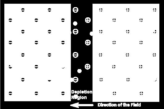
19 PN JUNCTION

20 PN JUNCTION

21 PN JUNCTION
22 SOLAR CELL OPERATION Basic steps: the generation of light-generated carriers; the collection of the light-generated carries to generate a current; the generation of a voltage across the solar cell; and the dissipation of power in the load and in parasitic resistances.
23 SOLAR CELL OPERATION
24 Normalized generation SOLAR CELL OPERATION Basic steps: the generation of light-generated carriers Red Blue Green Depth into cell
25 SOLAR CELL OPERATION Basic steps: the generation of light-generated carriers


26 SOLAR CELL OPERATION Basic steps: the collection of the carriers


27 SOLAR CELL OPERATION Basic steps: the collection of the carriers
28 Solar cell operation Quantum efficiency Ratio of the number of carriers collected to the number of photons of a given energy incident

29 Solar cell operation Quantum efficiency External quantum efficiency includes the effect of optical losses, e.g. reflection on the surface,...
 is measured Quantum Efficiency (QE) is calculated from")
30 SOLAR CELL OPERATION Spectral response Ratio of the current generated by the solar cell to the power incident on the solar cell Spectral Response (SR) is measured Quantum Efficiency (QE) is calculated from SR:
31 SOLAR CELL OPERATION Solar cell parameters IV characteristic = diode + light generated current
32 SOLAR CELL OPERATION Solar cell parameters IV characteristic

33 SOLAR CELL OPERATION Solar cell parameters IV characteristic

34 SOLAR CELL OPERATION Solar cell parameters IV characteristic


35 SOLAR CELL OPERATION Solar cell parameters IV characteristic
")
36 SOLAR CELL OPERATION Solar cell parameters IV characteristic: Short Circuit Current (I sc )
37 SOLAR CELL OPERATION Solar cell parameters IV characteristic: Short Circuit Current (I sc ) Area of the solar cell (common to use J sc in ma/cm 2 ) Incident flux (i.e. number of photons) Spectrum incident light Optical properties of the solar cell Collection probability, e.g. diffusion length
38 SOLAR CELL OPERATION Solar cell parameters IV characteristic: Open circuit voltage (V oc ) V oc depends strongly on the recombination
39 SOLAR CELL OPERATION Solar cell parameters IV characteristic: Maximum power I MP V MP

40 SOLAR CELL OPERATION Solar cell parameters IV characteristic: Fill factor (FF)
41 SOLAR CELL OPERATION Solar cell parameters Efficiency (η) is the fraction of incident power which is converted to electricity
42 SOLAR CELL OPERATION Solar cell parameters Resistive effects Characteristic resistance Parasitic resistance
43 SOLAR CELL OPERATION Solar cell parameters Resistive effects Characteristic resistance Maximum power transfer is R LOAD = R CH

44 SOLAR CELL OPERATION Solar cell parameters Resistive effects Characteristic resistance Parasitic resistance Series resistance Shunt resistance
45 SOLAR CELL OPERATION Solar cell parameters Resistive effects Characteristic resistance Parasitic resistance Series resistance Shunt resistance
46 SOLAR CELL OPERATION Effect of the series resistance with I sc Medium Rs Large Rs V oc Slope of the I-V curve near V oc gives indication about R s
47 SOLAR CELL OPERATION Effect of the shunt resistance with I sc Medium R sh Large R sh V oc Slope of the I-V curve near Isc gives indication about Rsh
48 Current SOLAR CELL OPERATION Effect of irradiation Voltage
49 Current SOLAR CELL OPERATION Effect of temperature Temperature increase reduces voltage by 2.2 mv/ o C Voltage

50 DESIGN OF Si SOLAR CELL


51 DESIGN OF Si SOLAR CELL Optical losses - light which could have generated an electron-hole pair, but does not, because the light is reflected from the front surface, or because it is not absorbed in the solar cell.
52 DESIGN OF Si SOLAR CELL Optical losses - light which could have generated an electron-hole pair, but does not, because the light is reflected from the front surface, or because it is not absorbed in the solar cell. Top contact shading Top surface reflection Not enought optical path for photon absorption

53 DESIGN OF Si SOLAR CELL Optical losses Reduce shading from top contacts


54 DESIGN OF Si SOLAR CELL Optical losses Reduce shading from top contacts


55 DESIGN OF Si SOLAR CELL Optical losses Reduce shading from top contacts May increase series resistance Other emitter contact concepts becoming fashionable (burried or back contacts)
56 DESIGN OF Si SOLAR CELL Optical losses Anti-reflective coating 4 1 d n n n n n n n R Silicon ( n 2 ) Air ( n 0 ) ARC ( n 1 )
57 DESIGN OF Si SOLAR CELL Optical losses Anti-reflective coating

58 DESIGN OF Si SOLAR CELL Optical losses Surface texturing


59 DESIGN OF Si SOLAR CELL Optical losses Surface texturing Single crystal: Random pyramids, by etching Multi crystal: texturing by photolithography Single crystal: Inverted pyramids, by etching Multi crystal: texturing by macroporous silicon

60 DESIGN OF Si SOLAR CELL Optical losses Light trapping: increase optical length
61 DESIGN OF Si SOLAR CELL Optical losses Light trapping: increase optical length
62 DESIGN OF Si SOLAR CELL Optical losses Light trapping: increase optical length Snell s law of refraction:

63 DESIGN OF Si SOLAR CELL Optical losses Light trapping: increase optical length Snell s law of refraction:
64 DESIGN OF Si SOLAR CELL Optical losses Light trapping: increase optical length Snell s law of refraction:
65 DESIGN OF Si SOLAR CELL Optical losses In summary: Reduce front contact coverage Anti-reflective coating Surface texturing Light trapping
66 DESIGN OF Si SOLAR CELL Recombination losses Optimal conditions: the carrier must be generated within a diffusion length of the junction; the carrier must be generated closer to the junction than to hazardous recombination sites (unpassivated surface, grain boundary, )
67 DESIGN OF Si SOLAR CELL Recombination losses
 Increasing doping, creating a repelling field (decreases diffusion length thus not suitable for charge collection region; useful closer to contacts, e.g. Back Surface Field - BSF)")
68 Design of silicon solar cells Recombination losses: Surface passivation Reducing the number of dangling bonds by growing a SiO 2 or SiN thin film on the surface (also for anti-reflection coating; notice that it is an electric insulator) Increasing doping, creating a repelling field (decreases diffusion length thus not suitable for charge collection region; useful closer to contacts, e.g. Back Surface Field - BSF)

69 Design of silicon solar cells Recombination losses: Surface passivation
70 DESIGN OF Si SOLAR CELL Single junction silicon solar cell Best lab cell: 25% J. Zhao et al Novel 19.8% efficient honeycomb textured multicrystalline and 24.4% monocrystalline silicon solar cells. Applied Physics Letters 1998; 73: Best module: 23% M. Green et al, Solar Cell Efficiency Tables (Version 34) Prog. Photovolt: Res. Appl. 2009; 17: Practical cell design (for industry!) requires compromises, and thus lower efficiencies Check February issue of Photon International
71
72

73 DESIGN OF Si SOLAR CELL Practical cell design (for industry!) requires compromises, and thus lower efficiencies
74 Next class How to make a practical photovoltaic module Other (non-silicon) technologies A new set of exercises. And check
Electrons are shared in covalent bonds between atoms of Si. A bound electron has the lowest energy state.
 Photovoltaics Basic Steps the generation of light-generated carriers; the collection of the light-generated carriers to generate a current; the generation of a large voltage across the solar cell; and
EE 5611 Introduction to Microelectronic Technologies Fall Tuesday, September 23, 2014 Lecture 07
 EE 5611 Introduction to Microelectronic Technologies Fall 2014 Tuesday, September 23, 2014 Lecture 07 1 Introduction to Solar Cells Topics to be covered: Solar cells and sun light Review on semiconductor
Solar cells operation
 Solar cells operation photovoltaic effect light and dark V characteristics effect of intensity effect of temperature efficiency efficency losses reflection recombination carrier collection and quantum
ET3034TUx Utilization of band gap energy
 ET3034TUx - 3.3.1 - Utilization of band gap energy In the last two weeks we have discussed the working principle of a solar cell and the external parameters that define the performance of a solar cell.
3.1 Introduction to Semiconductors. Y. Baghzouz ECE Department UNLV
 3.1 Introduction to Semiconductors Y. Baghzouz ECE Department UNLV Introduction In this lecture, we will cover the basic aspects of semiconductor materials, and the physical mechanisms which are at the
February 1, 2011 The University of Toledo, Department of Physics and Astronomy SSARE, PVIC
 FUNDAMENTAL PROPERTIES OF SOLAR CELLS February 1, 2011 The University of Toledo, Department of Physics and Astronomy SSARE, PVIC Principles and Varieties of Solar Energy (PHYS 4400) and Fundamentals of
EE495/695 Introduction to Semiconductors I. Y. Baghzouz ECE Department UNLV
 EE495/695 Introduction to Semiconductors I Y. Baghzouz ECE Department UNLV Introduction Solar cells have always been aligned closely with other electronic devices. We will cover the basic aspects of semiconductor
Lab #5 Current/Voltage Curves, Efficiency Measurements and Quantum Efficiency
 Lab #5 Current/Voltage Curves, Efficiency Measurements and Quantum Efficiency R.J. Ellingson and M.J. Heben November 4, 2014 PHYS 4580, 6280, and 7280 Simple solar cell structure The Diode Equation Ideal
FYS 3028/8028 Solar Energy and Energy Storage. Calculator with empty memory Language dictionaries
 Faculty of Science and Technology Exam in: FYS 3028/8028 Solar Energy and Energy Storage Date: 11.05.2016 Time: 9-13 Place: Åsgårdvegen 9 Approved aids: Type of sheets (sqares/lines): Number of pages incl.
Fundamentals of Photovoltaics: C1 Problems. R.Treharne, K. Durose, J. Major, T. Veal, V.
 Fundamentals of Photovoltaics: C1 Problems R.Treharne, K. Durose, J. Major, T. Veal, V. Dhanak @cdtpv November 3, 2015 These problems will be highly relevant to the exam that you will sit very shortly.
Chapter 7. Solar Cell
 Chapter 7 Solar Cell 7.0 Introduction Solar cells are useful for both space and terrestrial application. Solar cells furnish the long duration power supply for satellites. It converts sunlight directly
Photovoltaic cell and module physics and technology. Vitezslav Benda, Prof Czech Technical University in Prague
 Photovoltaic cell and module physics and technology Vitezslav Benda, Prof Czech Technical University in Prague benda@fel.cvut.cz www.fel.cvut.cz 1 Outlines Photovoltaic Effect Photovoltaic cell structure
Toward a 1D Device Model Part 1: Device Fundamentals
 Toward a 1D Device Model Part 1: Device Fundamentals Lecture 7 9/29/2011 MIT Fundamentals of Photovoltaics 2.626/2.627 Fall 2011 Prof. Tonio Buonassisi 1 Learning Objectives: Toward a 1D Device Model 1.
Photovoltaic cell and module physics and technology
 Photovoltaic cell and module physics and technology Vitezslav Benda, Prof Czech Technical University in Prague benda@fel.cvut.cz www.fel.cvut.cz 6/21/2012 1 Outlines Photovoltaic Effect Photovoltaic cell
smal band gap Saturday, April 9, 2011
 small band gap upper (conduction) band empty small gap valence band filled 2s 2p 2s 2p hybrid (s+p)band 2p no gap 2s (depend on the crystallographic orientation) extrinsic semiconductor semi-metal electron
Comparison of Ge, InGaAs p-n junction solar cell
 ournal of Physics: Conference Series PAPER OPEN ACCESS Comparison of Ge, InGaAs p-n junction solar cell To cite this article: M. Korun and T. S. Navruz 16. Phys.: Conf. Ser. 77 135 View the article online
Technology Options for Photo voltaic Solar Cells. Claudio Fiegna
 Technology Options for Photo voltaic Solar Cells Claudio Fiegna Outline Introduction Working principle for solar cells Silicon based solar cells Crystalline Thin film a Si or c Si Other thin film technologies
SEMICONDUCTOR PHYSICS REVIEW BONDS,
 SEMICONDUCTOR PHYSICS REVIEW BONDS, BANDS, EFFECTIVE MASS, DRIFT, DIFFUSION, GENERATION, RECOMBINATION February 3, 2011 The University of Toledo, Department of Physics and Astronomy SSARE, PVIC Principles
Carrier Recombination
 Notes for ECE-606: Spring 013 Carrier Recombination Professor Mark Lundstrom Electrical and Computer Engineering Purdue University, West Lafayette, IN USA lundstro@purdue.edu /19/13 1 carrier recombination-generation
ET3034TUx External parameters of an ideal solar cell. How can we determine the performance of a solar cell?
 ET3034TUx - 3.2.1 - External parameters of an ideal solar cell How can we determine the performance of a solar cell? In the previous block we have introduced the J- V curve of an ideal solar cell and its
Thermionic Current Modeling and Equivalent Circuit of a III-V MQW P-I-N Photovoltaic Heterostructure
 Thermionic Current Modeling and Equivalent Circuit of a III-V MQW P-I-N Photovoltaic Heterostructure ARGYRIOS C. VARONIDES Physics and Electrical Engineering Department University of Scranton 800 Linden
High efficiency silicon and perovskite-silicon solar cells for electricity generation
 High efficiency silicon and perovskite-silicon solar cells for electricity generation Ali Dabirian Email: dabirian@ipm.ir 1 From Solar Energy to Electricity 2 Global accumulative PV installed In Iran it
The photovoltaic effect occurs in semiconductors where there are distinct valence and
 How a Photovoltaic Cell Works The photovoltaic effect occurs in semiconductors where there are distinct valence and conduction bands. (There are energies at which electrons can not exist within the solid)
(Co-PIs-Mark Brongersma, Yi Cui, Shanhui Fan) Stanford University. GCEP Research Symposium 2013 Stanford, CA October 9, 2013
 Stanford University. GCEP Research Symposium 2013 Stanford, CA October 9, 2013") High-efficiency thin film nano-structured multi-junction solar James S. cells Harris (PI) (Co-PIs-Mark Brongersma, Yi Cui, Shanhui Fan) Stanford University GCEP Research Symposium 2013 Stanford, CA October
High-efficiency thin film nano-structured multi-junction solar James S. cells Harris (PI) (Co-PIs-Mark Brongersma, Yi Cui, Shanhui Fan) Stanford University GCEP Research Symposium 2013 Stanford, CA October
Photovoltaic Energy Conversion. Frank Zimmermann
 Photovoltaic Energy Conversion Frank Zimmermann Solar Electricity Generation Consumes no fuel No pollution No greenhouse gases No moving parts, little or no maintenance Sunlight is plentiful & inexhaustible
A. K. Das Department of Physics, P. K. College, Contai; Contai , India.
 IOSR Journal of Applied Physics (IOSR-JAP) e-issn: 2278-4861.Volume 7, Issue 2 Ver. II (Mar. - Apr. 2015), PP 08-15 www.iosrjournals.org Efficiency Improvement of p-i-n Structure over p-n Structure and
Nanophotonics: solar and thermal applications
 Nanophotonics: solar and thermal applications Shanhui Fan Ginzton Laboratory and Department of Electrical Engineering Stanford University http://www.stanford.edu/~shanhui Nanophotonic Structures Photonic
EE 6313 Homework Assignments
 EE 6313 Homework Assignments 1. Homework I: Chapter 1: 1.2, 1.5, 1.7, 1.10, 1.12 [Lattice constant only] (Due Sept. 1, 2009). 2. Homework II: Chapter 1, 2: 1.17, 2.1 (a, c) (k = π/a at zone edge), 2.3
The Opto-Electronic Physics That Just Broke the Efficiency Record in Solar Cells
 The Opto-Electronic Physics That Just Broke the Efficiency Record in Solar Cells Solar Energy Mini-Series Jen-Hsun Huang Engineering Center Stanford, California Sept. 26, 2011 Owen D. Miller & Eli Yablonovitch
Maria Carmela Di Piazza. Gianpaolo Vitale. Photovoltaic Sources. Modeling and Emulation. ^ Springer
 Maria Carmela Di Piazza Gianpaolo Vitale Photovoltaic Sources Modeling and Emulation ^ Springer Part I 1 From the Nuclear Fusion to the Radiated Energy on the Earth... 3 1.1 Inside the Universe 3 1.2 The
OPTI510R: Photonics. Khanh Kieu College of Optical Sciences, University of Arizona Meinel building R.626
 OPTI510R: Photonics Khanh Kieu College of Optical Sciences, University of Arizona kkieu@optics.arizona.edu Meinel building R.626 Announcements Homework #6 is assigned, due May 1 st Final exam May 8, 10:30-12:30pm
Lecture 5 Junction characterisation
 Lecture 5 Junction characterisation Jon Major October 2018 The PV research cycle Make cells Measure cells Despair Repeat 40 1.1% 4.9% Data Current density (ma/cm 2 ) 20 0-20 -1.0-0.5 0.0 0.5 1.0 Voltage
The Role of doping in the window layer on Performance of a InP Solar Cells USING AMPS-1D
 IOSR Journal of Engineering (IOSRJEN) ISSN: 2250-3021 Volume 2, Issue 8(August 2012), PP 42-46 The Role of doping in the window layer on Performance of a InP Solar Cells USING AMPS-1D Dennai Benmoussa
Keywords: APSYS; GaInP/GaAs/InGaAs/InGaAs four-junction solar cell; theoretical simulation
 2016 International Conference on Power Engineering & Energy, Environment (PEEE 2016) ISBN: 978-1-60595-376-2 2-simulation of Inverted Metamorphic GaInP/Gas/In 0.3 Ga 0.7 s/in 0.58 Ga 0.42 s Four-unction
Electron Energy, E E = 0. Free electron. 3s Band 2p Band Overlapping energy bands. 3p 3s 2p 2s. 2s Band. Electrons. 1s ATOM SOLID.
 Electron Energy, E Free electron Vacuum level 3p 3s 2p 2s 2s Band 3s Band 2p Band Overlapping energy bands Electrons E = 0 1s ATOM 1s SOLID In a metal the various energy bands overlap to give a single
Graded S i N x /S i O x N y Layers as Antireflective Coatings for Solar Cells Based on GaAs and Silicon Crystalline
 Science Research 2016; 4(1): 21-25 Published online February 25, 2016 (http://www.sciencepublishinggroup.com/j/sr) doi: 10.11648/j.sr.20160401.14 ISSN: 2329-0935 (Print); ISSN: 2329-0927 (Online) Graded
EE 446/646 Photovoltaic Devices I. Y. Baghzouz
 EE 446/646 Photovoltaic Devices I Y. Baghzouz What is Photovoltaics? First used in about 1890, the word has two parts: photo, derived from the Greek word for light, volt, relating to electricity pioneer
DEVICE CHARACTERIZATION OF (AgCu)(InGa)Se 2 SOLAR CELLS
(InGa)Se 2 SOLAR CELLS") DEVICE CHARACTERIZATION OF (AgCu)(InGa)Se 2 SOLAR CELLS William Shafarman 1, Christopher Thompson 1, Jonathan Boyle 1, Gregory Hanket 1, Peter Erslev 2, J. David Cohen 2 1 Institute of Energy Conversion,
DEVICE CHARACTERIZATION OF (AgCu)(InGa)Se 2 SOLAR CELLS William Shafarman 1, Christopher Thompson 1, Jonathan Boyle 1, Gregory Hanket 1, Peter Erslev 2, J. David Cohen 2 1 Institute of Energy Conversion,
Third generation solar cells - How to use all the pretty colours?
 Third generation solar cells - How to use all the pretty colours? Erik Stensrud Marstein Department for Solar Energy Overview The trouble with conventional solar cells Third generation solar cell concepts
Chemistry Instrumental Analysis Lecture 8. Chem 4631
 Chemistry 4631 Instrumental Analysis Lecture 8 UV to IR Components of Optical Basic components of spectroscopic instruments: stable source of radiant energy transparent container to hold sample device
Photodiodes and other semiconductor devices
 Photodiodes and other semiconductor devices Chem 243 Winter 2017 What is a semiconductor? no e - Empty e levels Conduction Band a few e - Empty e levels Filled e levels Filled e levels lots of e - Empty
Solar Cell Physics: recombination and generation
 NCN Summer School: July 2011 Solar Cell Physics: recombination and generation Prof. Mark Lundstrom lundstro@purdue.edu Electrical and Computer Engineering Purdue University West Lafayette, Indiana USA
Electronic Supplementary Information. Recombination kinetics in silicon solar cell under low-concentration: Electroanalytical
 Electronic Supplementary Material (ESI) for Physical Chemistry Chemical Physics. This journal is the Owner Societies 2014 Electronic Supplementary Information Recombination kinetics in silicon solar cell
Solar Photovoltaics & Energy Systems
 Solar Photovoltaics & Energy Systems Lecture 3. Crystalline Semiconductor Based Solar Cells ChE-600 Wolfgang Tress, March 2018 1 Photovoltaic Solar Energy Conversion 2 Outline Recap: Thermodynamics of
Solar Cells Technology: An Engine for National Development
 IOSR Journal of Electrical and Electronics Engineering (IOSR-JEEE) e-issn: 2278-1676,p-ISSN: 2320-3331, Volume 7, Issue 5 (Sep. - Oct. 2013), PP 13-18 Solar Cells Technology: An Engine for National Development
Photon Extraction: the key physics for approaching solar cell efficiency limits
 Photon Extraction: the key physics for approaching solar cell efficiency limits Owen Miller*: Post-doc, MIT Math Eli Yablonovitch: UC Berkeley, LBNL Slides/Codes/Relevant Papers: math.mit.edu/~odmiller/publications
3.1 Absorption and Transparency
 3.1 Absorption and Transparency 3.1.1 Optical Devices (definitions) 3.1.2 Photon and Semiconductor Interactions 3.1.3 Photon Intensity 3.1.4 Absorption 3.1 Absorption and Transparency Objective 1: Recall
In this block the two transport mechanisms will be discussed: diffusion and drift.
 ET3034TUx - 2.3.3 Transport of charge carriers What are the charge carrier transport principles? In this block the two transport mechanisms will be discussed: diffusion and drift. We will discuss that
Silicon Concentrator Solar Cells: Fabrication, Characterization and Development of Innovative Designs.
 University of Trento Department of Physics Doctoral School in Physics, XXV cycle Phd Thesis Silicon Concentrator Solar Cells: Fabrication, Characterization and Development of Innovative Designs. Candidate:
1 Name: Student number: DEPARTMENT OF PHYSICS AND PHYSICAL OCEANOGRAPHY MEMORIAL UNIVERSITY OF NEWFOUNDLAND. Fall :00-11:00
 1 Name: DEPARTMENT OF PHYSICS AND PHYSICAL OCEANOGRAPHY MEMORIAL UNIVERSITY OF NEWFOUNDLAND Final Exam Physics 3000 December 11, 2012 Fall 2012 9:00-11:00 INSTRUCTIONS: 1. Answer all seven (7) questions.
LEC E T C U T R U E R E 17 -Photodetectors
 LECTURE 17 -Photodetectors Topics to be covered Photodetectors PIN photodiode Avalanche Photodiode Photodetectors Principle of the p-n junction Photodiode A generic photodiode. Photodetectors Principle
Lecture 15: Optoelectronic devices: Introduction
 Lecture 15: Optoelectronic devices: Introduction Contents 1 Optical absorption 1 1.1 Absorption coefficient....................... 2 2 Optical recombination 5 3 Recombination and carrier lifetime 6 3.1
Semiconductor Physical Electronics
 Semiconductor Physical Electronics Sheng S. Li Department of Electrical Engineering University of Florida Gainesville, Florida Plenum Press New York and London Contents CHAPTER 1. Classification of Solids
Fundamentals of Light Trapping
 Fundamentals of Light Trapping James R. Nagel, PhD November 16, 2017 Salt Lake City, Utah About Me PhD, Electrical Engineering, University of Utah (2011) Research Associate for Dept. of Metallurgical Engineering
Optimization of the Properties of the Back Surface Field of a Cu(In,Ga)Se 2 Thin Film Solar Cell
Se 2 Thin Film Solar Cell") American Journal of Energy Research, 2017, Vol. 5, No. 2, 57-62 Available online at http://pubs.sciepub.com/ajer/5/2/5 Science and Education Publishing DOI:10.12691/ajer-5-2-5 Optimization of the Properties
American Journal of Energy Research, 2017, Vol. 5, No. 2, 57-62 Available online at http://pubs.sciepub.com/ajer/5/2/5 Science and Education Publishing DOI:10.12691/ajer-5-2-5 Optimization of the Properties
Toward a 1D Device Model Part 2: Material Fundamentals
 Toward a 1D Device Model Part 2: Material Fundamentals Lecture 8 10/4/2011 MIT Fundamentals of Photovoltaics 2.626/2.627 Fall 2011 Prof. Tonio Buonassisi 1 2.626/2.627 Roadmap You Are Here 2 2.626/2.627:
Semiconductors and Optoelectronics. Today Semiconductors Acoustics. Tomorrow Come to CH325 Exercises Tours
 Semiconductors and Optoelectronics Advanced Physics Lab, PHYS 3600 Don Heiman, Northeastern University, 2017 Today Semiconductors Acoustics Tomorrow Come to CH325 Exercises Tours Semiconductors and Optoelectronics
Semiconductor Devices and Circuits Fall Midterm Exam. Instructor: Dr. Dietmar Knipp, Professor of Electrical Engineering. Name: Mat. -Nr.
 Semiconductor Devices and Circuits Fall 2003 Midterm Exam Instructor: Dr. Dietmar Knipp, Professor of Electrical Engineering Name: Mat. -Nr.: Guidelines: Duration of the Midterm: 1 hour The exam is a closed
Solar Photovoltaics & Energy Systems
 Solar Photovoltaics & Energy Systems Lecture 4. Crystalline Semiconductor Based Solar Cells ChE-600 Wolfgang Tress, May 2016 1 Photovoltaic Solar Energy Conversion 2 Semiconductor vs. Heat Engine spectral
3.003 Principles of Engineering Practice
 3.003 Principles of Engineering Practice One Month Review Solar Cells The Sun Semiconductors pn junctions Electricity 1 Engineering Practice 1. Problem Definition 2. Constraints 3. Options 4. Analysis
Course overview. Me: Dr Luke Wilson. The course: Physics and applications of semiconductors. Office: E17 open door policy
 Course overview Me: Dr Luke Wilson Office: E17 open door policy email: luke.wilson@sheffield.ac.uk The course: Physics and applications of semiconductors 10 lectures aim is to allow time for at least one
Organic Electronic Devices
 Organic Electronic Devices Week 4: Organic Photovoltaic Devices Lecture 4.2: Characterizing Device Parameters in OPVs Bryan W. Boudouris Chemical Engineering Purdue University 1 Lecture Overview and Learning
Classification of Solids
 Classification of Solids Classification by conductivity, which is related to the band structure: (Filled bands are shown dark; D(E) = Density of states) Class Electron Density Density of States D(E) Examples
Quiz #1 Practice Problem Set
 Name: Student Number: ELEC 3908 Physical Electronics Quiz #1 Practice Problem Set? Minutes January 22, 2016 - No aids except a non-programmable calculator - All questions must be answered - All questions
Sheng S. Li. Semiconductor Physical Electronics. Second Edition. With 230 Figures. 4) Springer
 Springer") Sheng S. Li Semiconductor Physical Electronics Second Edition With 230 Figures 4) Springer Contents Preface 1. Classification of Solids and Crystal Structure 1 1.1 Introduction 1 1.2 The Bravais Lattice
Sheng S. Li Semiconductor Physical Electronics Second Edition With 230 Figures 4) Springer Contents Preface 1. Classification of Solids and Crystal Structure 1 1.1 Introduction 1 1.2 The Bravais Lattice
MODELING THE FUNDAMENTAL LIMIT ON CONVERSION EFFICIENCY OF QD SOLAR CELLS
 MODELING THE FUNDAMENTAL LIMIT ON CONVERSION EFFICIENCY OF QD SOLAR CELLS Ա.Մ.Կեչիյանց Ara Kechiantz Institute of Radiophysics and Electronics (IRPhE), National Academy of Sciences (Yerevan, Armenia) Marseille
Introduction. Katarzyna Skorupska. Silicon will be used as the model material however presented knowledge applies to other semiconducting materials
 Introduction Katarzyna Skorupska Silicon will be used as the model material however presented knowledge applies to other semiconducting materials 2 June 26 Intrinsic and Doped Semiconductors 3 July 3 Optical
Supplementary Figure 1. Supplementary Figure 1 Characterization of another locally gated PN junction based on boron
 Supplementary Figure 1 Supplementary Figure 1 Characterization of another locally gated PN junction based on boron nitride and few-layer black phosphorus (device S1). (a) Optical micrograph of device S1.
Appendix 1: List of symbols
 Appendix 1: List of symbols Symbol Description MKS Units a Acceleration m/s 2 a 0 Bohr radius m A Area m 2 A* Richardson constant m/s A C Collector area m 2 A E Emitter area m 2 b Bimolecular recombination
Lecture 4 - Carrier generation and recombination. February 12, 2007
 6.720J/3.43J - Integrated Microelectronic Devices - Spring 2007 Lecture 4-1 Contents: Lecture 4 - Carrier generation and recombination 1. G&R mechanisms February 12, 2007 2. Thermal equilibrium: principle
Electronics The basics of semiconductor physics
 Electronics The basics of semiconductor physics Prof. Márta Rencz, Gergely Nagy BME DED September 16, 2013 The basic properties of semiconductors Semiconductors conductance is between that of conductors
Basic Semiconductor Physics
 6 Basic Semiconductor Physics 6.1 Introduction With this chapter we start with the discussion of some important concepts from semiconductor physics, which are required to understand the operation of solar
Boosting the Performance of Solar Cells with Intermediate Band Absorbers The Case of ZnTe:O
 Journal of Energy and Power Engineering 11 (2017) 417-426 doi: 10.17265/1934-8975/2017.06.007 D DAVID PUBLISHING Boosting the Performance of Solar Cells with Intermediate Band Absorbers The Case of ZnTe:O
Metal Vapour Lasers Use vapoured metal as a gain medium Developed by W. Silfvast (1966) Two types: Ionized Metal vapour (He-Cd) Neutral Metal vapour
 Two types: Ionized Metal vapour (He-Cd) Neutral Metal vapour") Metal Vapour Lasers Use vapoured metal as a gain medium Developed by W. Silfvast (1966) Two types: Ionized Metal vapour (He-Cd) Neutral Metal vapour (Cu) All operate by vaporizing metal in container Helium
Metal Vapour Lasers Use vapoured metal as a gain medium Developed by W. Silfvast (1966) Two types: Ionized Metal vapour (He-Cd) Neutral Metal vapour (Cu) All operate by vaporizing metal in container Helium
Qualitative Picture of the Ideal Diode. G.R. Tynan UC San Diego MAE 119 Lecture Notes
 Qualitative Picture of the Ideal Diode G.R. Tynan UC San Diego MAE 119 Lecture Notes Band Theory of Solids: From Single Attoms to Solid Crystals Isolated Li atom (conducting metal) Has well-defined, isolated
EECS130 Integrated Circuit Devices
 EECS130 Integrated Circuit Devices Professor Ali Javey 8/30/2007 Semiconductor Fundamentals Lecture 2 Read: Chapters 1 and 2 Last Lecture: Energy Band Diagram Conduction band E c E g Band gap E v Valence
Supplemental Discussion for Multijunction Solar Cell Efficiencies: Effect of Spectral Window, Optical Environment and Radiative Coupling
 Electronic Supplementary Material (ESI) for Energy & Environmental Science. This journal is The Royal Society of Chemistry 2014 Supplemental Discussion for Multijunction Solar Cell Efficiencies: Effect
5. Semiconductors and P-N junction
 5. Semiconductors and P-N junction Thomas Zimmer, University of Bordeaux, France Summary Learning Outcomes... 2 Physical background of semiconductors... 2 The silicon crystal... 2 The energy bands... 3
AMPS - 1D. A. K. Das Department of Physics, P. K. College, Contai; Contai , India.
 IOSR Journal of Applied Physics (IOSRJAP) eissn: 22784861.Volume 7, Issue 1 Ver. II (Jan.Feb. 2015), PP 2330 www.iosrjournals.org Numerical Simulation of Si 1 x Ge x Thin Film Solar Cell Using AMPS 1D
Graded SiO x N y layers as antireflection coatings for solar cells application
 Materials Science-Poland, Vol. 24, No. 4, 2006 Graded SiO x N y layers as antireflection coatings for solar cells application M. LIPIŃSKI 1*, S. KLUSKA 2, H. CZTERNASTEK 2, P. ZIĘBA 1 1 Institute of Metallurgy
ESE 372 / Spring 2013 / Lecture 5 Metal Oxide Semiconductor Field Effect Transistor
 Metal Oxide Semiconductor Field Effect Transistor V G V G 1 Metal Oxide Semiconductor Field Effect Transistor We will need to understand how this current flows through Si What is electric current? 2 Back
Temperature Dependent Current-voltage Characteristics of P- type Crystalline Silicon Solar Cells Fabricated Using Screenprinting
 Temperature Dependent Current-voltage Characteristics of P- type Crystalline Silicon Solar Cells Fabricated Using Screenprinting Process Hyun-Jin Song, Won-Ki Lee, Chel-Jong Choi* School of Semiconductor
Physics of the thermal behavior of photovoltaic cells
 Physics of the thermal behavior of photovoltaic cells O. Dupré *,2, Ph.D. candidate R. Vaillon, M. Green 2, advisors Université de Lyon, CNRS, INSA-Lyon, UCBL, CETHIL, UMR58, F-6962 Villeurbanne, France
Introduction to Transistors. Semiconductors Diodes Transistors
 Introduction to Transistors Semiconductors Diodes Transistors 1 Semiconductors Typical semiconductors, like silicon and germanium, have four valence electrons which form atomic bonds with neighboring atoms
Quiz #1 Due 9:30am Session #10. Quiz Instructions
 2.626/2.627 Fall 2011 Fundamentals of Photovoltaics Quiz #1 Due 9:30am Session #10 Quiz Instructions The undergraduate version of this quiz (2.627) consists of four (4) multipart questions for a point
High resolution THz scanning for optimization of dielectric layer opening process on doped Si surfaces
 High resolution THz scanning for optimization of dielectric layer opening process on doped Si surfaces P. Spinelli 1, F.J.K. Danzl 1, D. Deligiannis 1,2, N. Guillevin 1, A.R. Burgers 1, S. Sawallich 3,
Analyze the effect of window layer (AlAs) for increasing the efficiency of GaAs based solar cell
 for increasing the efficiency of GaAs based solar cell") American Journal of Engineering Research (AJER) e-issn: 2320-0847 p-issn : 2320-0936 Volume-4, Issue-7, pp-304-315 www.ajer.org Research Paper Open Access Analyze the effect of window layer (AlAs) for
American Journal of Engineering Research (AJER) e-issn: 2320-0847 p-issn : 2320-0936 Volume-4, Issue-7, pp-304-315 www.ajer.org Research Paper Open Access Analyze the effect of window layer (AlAs) for
electronics fundamentals
 electronics fundamentals circuits, devices, and applications THOMAS L. FLOYD DAVID M. BUCHLA Lesson 1: Diodes and Applications Semiconductors Figure 1-1 The Bohr model of an atom showing electrons in orbits
Lecture 6 Optical Characterization of Inorganic Semiconductors Dr Tim Veal, Stephenson Institute for Renewable Energy and Department of Physics,
 Lecture 6 Optical Characterization of Inorganic Semiconductors Dr Tim Veal, Stephenson Institute for Renewable Energy and Department of Physics, University of Liverpool Lecture Outline Lecture 6: Optical
Chapter 6 Solar Cells (Supplementary)
") 1 Chapter 6 olar Cells (upplementary) Chapter 6... 1 olar Cells... 1 6.1.1... 6.1.... 6.1.3... 6.1.4 Effect of Minority Electron Lifetime on Efficiency... 6.1.5 Effect of Minority hole Lifetime on Efficiency...
1 Chapter 6 olar Cells (upplementary) Chapter 6... 1 olar Cells... 1 6.1.1... 6.1.... 6.1.3... 6.1.4 Effect of Minority Electron Lifetime on Efficiency... 6.1.5 Effect of Minority hole Lifetime on Efficiency...
Chapter 6: Light-Emitting Diodes
 Chapter 6: Light-Emitting Diodes Photoluminescence and electroluminescence Basic transitions Luminescence efficiency Light-emitting diodes Internal quantum efficiency External quantum efficiency Device
Semiconductor device structures are traditionally divided into homojunction devices
 0. Introduction: Semiconductor device structures are traditionally divided into homojunction devices (devices consisting of only one type of semiconductor material) and heterojunction devices (consisting
Chapter 5. Semiconductor Laser
 Chapter 5 Semiconductor Laser 5.0 Introduction Laser is an acronym for light amplification by stimulated emission of radiation. Albert Einstein in 1917 showed that the process of stimulated emission must
CME 300 Properties of Materials. ANSWERS: Homework 9 November 26, As atoms approach each other in the solid state the quantized energy states:
 CME 300 Properties of Materials ANSWERS: Homework 9 November 26, 2011 As atoms approach each other in the solid state the quantized energy states: are split. This splitting is associated with the wave
Lecture 8. Equations of State, Equilibrium and Einstein Relationships and Generation/Recombination
 Lecture 8 Equations of State, Equilibrium and Einstein Relationships and Generation/Recombination Reading: (Cont d) Notes and Anderson 2 sections 3.4-3.11 Energy Equilibrium Concept Consider a non-uniformly
Electronic Circuits for Mechatronics ELCT 609 Lecture 2: PN Junctions (1)
") Electronic Circuits for Mechatronics ELCT 609 Lecture 2: PN Junctions (1) Assistant Professor Office: C3.315 E-mail: eman.azab@guc.edu.eg 1 Electronic (Semiconductor) Devices P-N Junctions (Diodes): Physical
Electronic Circuits for Mechatronics ELCT 609 Lecture 2: PN Junctions (1) Assistant Professor Office: C3.315 E-mail: eman.azab@guc.edu.eg 1 Electronic (Semiconductor) Devices P-N Junctions (Diodes): Physical
Organic Electronic Devices
 Organic Electronic Devices Week 4: Organic Photovoltaic Devices Lecture 4.1: Overview of Organic Photovoltaic Devices Bryan W. Boudouris Chemical Engineering Purdue University 1 Lecture Overview and Learning
Question 1. (Marks 16)
") 5 Question 1. (Marks 16) Consider the circuit shown in the figure, where C 1 = 6.00µF, C 2 = 3.00µF, and V = 20.0V. Capacitor C 1 is first charged by closing switch S 1. Switch S 1 is then opened, and
5 Question 1. (Marks 16) Consider the circuit shown in the figure, where C 1 = 6.00µF, C 2 = 3.00µF, and V = 20.0V. Capacitor C 1 is first charged by closing switch S 1. Switch S 1 is then opened, and
Nanomaterials for Photovoltaics (v11) 14. Intermediate-Band Solar Cells
 14. Intermediate-Band Solar Cells") 1 14. Intermediate-Band Solar Cells Intermediate (impurity) band solar cells (IBSCs) (I) Concept first proposed by A. Luque and A. Martí in 1997. Establish an additional electronic band within the band
1 14. Intermediate-Band Solar Cells Intermediate (impurity) band solar cells (IBSCs) (I) Concept first proposed by A. Luque and A. Martí in 1997. Establish an additional electronic band within the band
Paper Review. Special Topics in Optical Engineering II (15/1) Minkyu Kim. IEEE Journal of Quantum Electronics, Feb 1985
 Minkyu Kim. IEEE Journal of Quantum Electronics, Feb 1985") Paper Review IEEE Journal of Quantum Electronics, Feb 1985 Contents Semiconductor laser review High speed semiconductor laser Parasitic elements limitations Intermodulation products Intensity noise Large
Paper Review IEEE Journal of Quantum Electronics, Feb 1985 Contents Semiconductor laser review High speed semiconductor laser Parasitic elements limitations Intermodulation products Intensity noise Large