An Introduction to NanoScience and NanoTechnology
|
|
|
- Sharyl West
- 5 years ago
- Views:
Transcription
1 An Introduction to NanoScience and NanoTechnology ELEC 6271/498X An Overview
2 Introduction Evolution of IC characteristics in order of magnitude from the time that the technology was introduced in 1960: In 1960 one transistor consisted of atoms In 2000 these reduced to 10 7 In 2010 it is expected to decrease by 10 3 Meanwhile the area of capacitors is reduced from 1 cm 2 to 0.01 micron 2 and reducing the voltage from 10V to 1V and below.
3 Introduction Golden Rule No matter what the size, make it smaller No matter what the speed, make it faster No matter what the function, make it larger No matter what the cost, make it cheaper No matter how little it heats up, make it cooler
4 Introduction The following factors helped the Golden Rule: 1) Reducing the size of the device 2) Enlarging the chip area 3) Increasing functional integration It is assumed that silicon technology has its limit for further miniaturization to approx 10 nm. Therefore to overcome this restriction we need to increase functionality integration or alternatively approaching nanoelectronics which offers integration level 2 to 4 orders larger than 10 nm technology. Emerging a new technology called Nanotechnology
5 Introduction No matter what form of electronic devices we have, we need to learn how to model and describe the electronic properties of the device. Due to the complexity of these structures (elements of the nanoelectronics) and the different nature of things at very low scales, one need to investigate and reexamine the characteristics of these structures. Sometimes are very different from their macro or micro counterparts. The physical, mechanical, chemical, and in general most properties of the materials will change once the size of the structures reduces to nano scale. As a result, a new science called nanoscience is emerging.
6 What is Nanotechnology? Nanotechnology deals with fabrication and structures of objects with dimensions in order of nanometers. Nanotechnology is the research and technology development at the atomic, molecular or macromolecular levels, in the length scale of approximately nanometer range. Nanoscale 10-9 meter
7 What is NanoScience? Nanoscience deals with sciences related to the systems structured by nanotechnology. Generally in the nanometer region, most physical, chemical, biological, mechanical, electrical etc. become size-dependent. For example, the color of a piece of gold remains golden until the piece it reduced to nanometer sizes. Similarly, the color of a piece of silicon wafer changes as its size reduces to nanometer. The same is true for their melting points or any other physical or chemical properties.
8 Nanotechnology Because properties at the nanoscale are sizedependent, nanoscale science and engineering offer an entirely new design motif for developing advanced materials and their applications. Nanotechnology deals with the creation of functional materials, devices and systems through control of matter on the nanometer length scale (1-100 nanometers), and ability to control them. Nanoscience deals with novel phenomena and properties (physical, chemical, biological, mechanical, electrical etc.) at that length scale.
9 Nanotechnology Nano and quantum computing, nano-formed components and nano-based wiring have been some of the focus areas. Research has led to some important developments: demonstration of Coulomb blockade, quantum effect, single electron memory and logic gates that operate at room temperature; integration of scanning probe tips into sizable arrays for lithographic and mechanical information storage applications; and fabrication of photonic band-gap structures. In addition, biological computing is becoming a possibility.
10 Nanotechnology Laws relating to physical, chemical, biological, electrical, magnetic and other properties at the nano-scale are different from those that apply to macro matter. It is the laws of quantum mechanics (and not classical mechanics) that apply at that scale.


11 Nanotechnology Human hair Nanotube FET Bacteria TR on IC Ant s eye segment Nano manipulation Scale (meters) Atom DNA NEMS MEMS 1/4/2005 ECE, Concordia 7
12 Why nanotechnology? Size Weight Cost Most importantly is Sensitivity. It is the surface to volume ratio in any nanostructure which makes this technology very attractive for many applications.
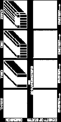
13 Nanostructures Elements of nanostructures: Quantum Dots (0 D) Quantum Wires (1 D) Quantum Walls (2 D) Nanoparticles (3 D)
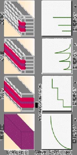
14 Quantum Structures When the size or dimension of a material is continuously reduced from a large or macroscopic size, such as a meter or a centimeter, to a very small size, the properties remain the same at first. Then small changes begin to occur, until finally when the size drops below l00nm, dramatic changes in properties can occur. If one dimension is reduced to the nano-range while the other two dimensions remain large, then we obtain a structure known as an extremely thin films, quantum well. If two dimensions are so reduced and one remains large, the resulting structure is referred to as a quantum wire. The extreme case of this process of size reduction in which all three dimensions reach the low nanometer range is called a quantum dot. The word quantum is associated with these three types of nanostructures because the changes in properties arise from the quantum-mechanical nature of physics in the domain of the ultra small.

15 Quantum Well
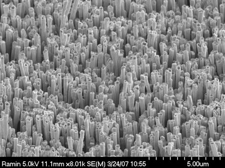
16 Nano Wires Metal/Semiconductor Nanowires A variety of quasi 1-D nano sized materials, like carbon nanotubes, porous silicon, GaAs, Silicon, Germanium nanowires, metal nanowires have been synthesized. These materials show physical properties different from those of the bulk. Create opportunities for fundamental studies and for potential nanodevice applications. One dimensional high speed field effect transistors and laser working at low-threshold current density and high gain were developed using GaAs and InAs nanowires. Nano-sized metal-semiconductor heterojunction using silicon nanowire connected with a carbon nanotube is fabricated.
17 Nanowires Self-Standing AuNWs
18 Nanostructures Quantum dots are small metal or semiconductor boxes that hold a well-defined number of electrons. The number of electrons may be adjusted. The problem of a particle moving in presence of external potentials is a standard-textbook example of quantum mechanics: For a fully three-dimensional confinement, the particle spectrum is known to break into a number of discrete eigenenergies. Atoms represent natural realization of such confined systems. Semiconductor quantum dots (or "artificial atoms", as they are sometimes called) are man-made realizations: Exploiting the most advanced tools of nano-fabrication or selfassembly, it has become possible to tailor dotconfinement potentials with a high degree of flexibility.
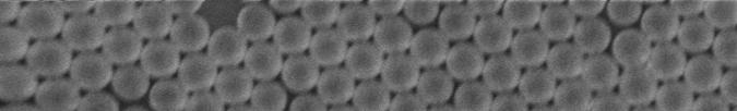
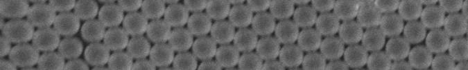
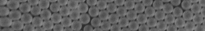
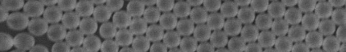
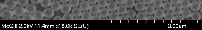
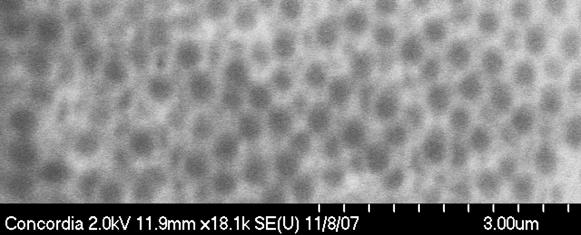
19 Nanoparticles MULTILAYERS OF PS MICROSPHERES AND Au NANOPARTICLES (AFM IMAGE) Poly Styrene microspheres: 510 nm; Au: 5 nm Vertical deposition 55 o C, 3 days
20 Nanostructures Physical Mechanical Electrical Chemical Biological Medical
21 Materials & Methods of Synthesis Semiconductor nanostructures (nanoparticles, nanowires, ) Metallic nanostructures
22 Semiconductors Nanostructures Semiconductor nanoparticles are unique for two very important reasons: As a semiconductor nanoparticle becomes smaller the ratio of the number of surface atoms to those in the interior increases, i.e. in very small particles greater than a third of all atoms reside on the surface. There is a change in the electronic properties of the material, as the size of the nanoparticle becomes smaller the band-gap becomes larger.
23 Semiconductors Nanostructures They are interesting because they have chemical and physical properties different from those of the bulk and isolated atoms and molecules with the same chemical composition. They provide opportunities to study the effect of spatial confinement and problems related to surfaces and interfaces. They can be fabricated in the form of Quantum Dots, Quantum Particles, nanowires or nanocrystals. They have unique electronics, magnetic and optical properties because of their small size and large surfaceto-volume ratio.
24 Semiconductors Nanostructures They have potential applications in a number of areas: Electronics Healthcare and Life Science Information and Communication Technologies, in light emitting diodes, single electron devices, quantum computing, photo-catalysis, non-linear optics, photo-electrochemistry, imaging science and electro-optics. Energy applications, solar cells. Fine Chemicals.
25 Synthesis Main challenge: control the size, shape, and surface properties (particles with single size, well-defined shape and surface characteristics). II-VI semiconductor materials, such as CdS, CdSe, ZnS can be prepared using wet colloidal chemistry methods both in single sized and surface passivated forms. They can be prepared in solutions, glasses and polymers. e.g. CdS Nanoparticles can be prepared in a number of environments by controlled mixing of Cd2+ ions with S2- ions in the presence of various acidic or basic stabilizers. Likewise, CdSe, CdTe, ZnS, ZnxCd1-xS, Mn-doped ZnS can be made using suitable precursors in different solvents. Metal oxide nanoparticles such as TiO2, ZnO and SnO2 can be prepared by forced hydrolysis techniques. Although difficult but preparation of III-V semiconductor nanocrystals of GaAs and InP has been possible.
26 Synthesis Chemical Vapor Deposition (CVD) Nanowires of Si, Ge, GaAs, InP Laser Ablation Carbon nanotubes, silicon nanowires, silica nanowires Carbon Nanotube Confined Reaction A technique which uses carbon nanotubes to fabricate variety of carbide nano-rods, like SiC, TiC, Fe3C. It is extended to synthesize nano-rods without carbon element, like GaN, Si3N4,.
27 Synthesis Vapor Phase Evaporation Many metal nanowires were prepared by this technique, like nanowires of Ag, Al, Au, Cu, Fe, Also some semiconductors nanowires like Si, Ge, ZnO, GeO2, GaSe, Electrochemical Deposition Three step approach: --preparation of nanopores on polycarbonate membrane film using heavy ion beam bombardment of the film. --electrochemical deposition of the metallic nanowires into the nanopores template. --lift-off of the nanowires by dissolving the membrane Self-assembly techniques


 a) V d =")
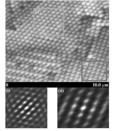
28 Self-Assembly Techniques S. Badilescu, M. Kahrizi, Journal of Materials Science: Materials, 2007 nanospheres colloidal crystal (a) a) V d = 100 µm/s b) Vd = 40 µm/s c) Vd = 15 µm/s (b) (c)

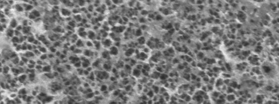
29 Nanocups Nanorings Nanoholes fabricated using Porous Silicon Method
30 Growth Mechanism of Nanowires The following growth mechanism will be discussed in detail. --Vapor-Liquid-Solid (VLS) Growth --Solution-Liquid-Solid (SLS) Growth --Vapor Phase Epitaxy
31 Nanowire systems The following nanowire materials and the method of their synthesis are discussed in detail --Si and Ge Nanowires --semiconductor Compound Nanowires; GaAs, InAs, GaN, ZnSe, ZnS, CdS, GaSe --Metal Nanowires --Oxide Nanowires; Silicon Oxide, Germanium Oxide, Gallium Oxide --Silicon Carbide, Silicon Nitride
32 Summary: Methods of Synthesis Nanoparticles Nanowires Scanning probe instruments like Atomic Force Microscope (AFM) Lithography Techniques: Dip-Pen Lithography E-Beam Lithography Ion-Beam Lithography Soft Lithography (nano printing) Plasma arcing Laser Ablation Chemical Vapor Deposition Electro-deposition Sol gel synthesis Ball milling, and the use of natural nanoparticles Self Assembly techniques 1. Top-Down Approach Thermal methods Chemical Methods Mechanical Methods Lithography Methods 2. Bottom-Up Approach Assemble from units Compact powders Solid-Solution precipitation Deposition and Coatings Electro-depositions
33 Characterization Spectroscopy, Microscopy and X-ray techniques are used to characterize the size, shape and surface properties of nanoparticles. UV visible, and Raman Spectroscopy, Scanning Tunneling Microscopy, Atomic Force Microscopy are used to characterize semiconductor nanoparticles. UV-visible spectroscopy is useful for characterizing optical properties of nanoparticles and for determining particle size. e.g. the spectra of CdS nanoparticles show a clear blue shift in the absorption onset for smaller particles compared to that of bulk CdS. This is due to the increase in effective band-gap with decreasing particle size. Transmission Electron Microscope can provide direct spatial resolution on the order of 0.1 nm and can be used to characterize the shape and lattice structures of nanoparticles. Photoluminescence
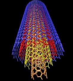
34 Carbon Nano Tubes (CNT) Carbon nanotubes are long, thin cylinders of carbon. These are large macromolecules that are unique for their size, shape, and remarkable physical properties. An ideal nanotube can be thought of as a single layer of graphite atoms arranged in hexagonal pattern that has been rolled up to make a cylinder. The tubes are tough and when bent or squeezed, spring back to their original shape.

35 CNT A single walled CNT

36 CNT To understand nanotube we need to know few basic terms. Considering the unrolled nanotube in figure above, the two unit vector â1 and â2 are defined as shown in the figure. The chiral vector of the nanotube, Ch, is defined as the vector normal to the circumference vector in the direction in which it is being i.e. Ch = nâ1 + mâ2
37 CNT Where â1 and â2 are unit vectors in the two-dimensional hexagonal lattice, and n and m are integers. The nanotubes are described by these numbers as (n, m). Another important parameter is the chiral angle, which is the angle between Ch and â1. If (n m) is divisible by 3 then the tube is metallic and if (n m) is not divisible by 3 then the tube is a semiconductor. On the basis of Cirality nanotubes can be divided in to three classes: Zigzag if either n = 0 or m = 0 Armchair if n = m Chiral if n m Armchair type is always metallic and the other two types can be either metallic or semiconductor depending on their Chiral condition.
38 CNT

39 CNT Different types nanotubes: a. Zigzag, b. Armchair, c. Chiral
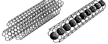
40 CNT Nanotubes have a very broad range of electronic, thermal, and structural properties that change depending on the different kinds of nanotube (defined by its diameter, length, and chirality, or twist). They can transfer heat very efficiently and more useful in the circuit as they can be cooled faster. They can be made to perform as a metal or a semiconductor depending on the way they are rolled. Nanotubes can have single cylindrical wall (SWNTs) or multiple walls (MWNTs) i.e. cylinders inside the other cylinders.
41 CNT
42 Carbon Nanotubes Production Processes Production processes for carbon nanotubes, vary from blasting carbon with an electrical arc or a laser to growing them from a vapor. These processes vary considerably with respect to the type of nanotube produced, quality, purity and scalability. Carbon nanotubes are usually created with the aid of a metal catalyst and this ends up as a contaminant with respect to many potential applications, especially in electronics. IBM has very recently, however, grown nanotubes on silicon structures without a metal catalyst. Fabrication techniques LASER EVAPORATION METHOD CARBON ARC METHOD CHEMICAL VAPOR DEPOSITION METHOD
43 Applications of Nanosystems Devices: The nano-devices are based upon various nanotechnologies. Carbon nanotube transistors Solid state quantum effect devices Molecular electronic devices Integration of those nanostructures together with MEMS technology is very promising for future photonic devices. Sensors (optical, biomedical, gas, ) Drug delivery Drug Discovery
44 Applications Carbon nanotube field effect transistors (CNFET) A carbon nanotube device is similar to a MOSFET where a gate is used to control the flow of current through the device by varying the field through a channel. The new idea here is the mechanism of transport of electrons from the source to drain. Instead of having a channel whose field can be controlled by a gate electrode, these devices have a tiny tubular structure of carbon nanotube. Carbon nanotube with diameter 2nm have extremely low resistance and thus can carry large current without heating, so it could be use as interconnectors. It also has very high thermal conductivity means that they can also serve as heat sink i.e. allows heat to be rapidly transferred away from the chip.

45 Applications CNFET A Carbon nanotube field effect transistors (CNFET)
46 Applications Single Electron Transistor The single electron transistor or SET is a new type of switching device that uses controlled electron tunneling to amplify current. An SET is made from two tunnel junctions that share a common electrode. A tunnel junction consists of two pieces of metal separated by a very thin (~1 nm) insulator as shown in the figure below. The only way for electrons in one of the metal electrodes to travel to the other electrode is to tunnel through the insulator. Since tunneling is a discrete process, the electric charge that flows through the tunnel junction flows in multiples of the charge of a single electron.


47 Applications SET A tunnel junction and its schematic diagram
48 SET A SET can be made by placing two tunnel junctions in series as shown in the figure below. It has double barrier potential. The double junction is a circuit consisting of two tunneling junction in series which forms an island between them called "Coulomb Island" that electrons can only enter by tunneling through one of the insulators. This device has three terminals like an ordinary field effect transistor: the outside terminal of each tunnel junction, and a "gate" terminal that is capacitively coupled to the node between the two tunnel junctions. The capacitor may seem like a third tunnel junction, but it is much thicker than the others so that no electrons can tunnel through it. The capacitor simply serves as a way of setting the electric charge on the Coulomb Island.
49 Applications Molecular Transistors

50 Applications Resonant Tunneling Diodes

51 Resonant Tunneling Transistor
52 Applications LEDs, Tunable lasers Researches have demonstrated that semiconducting quantum dots can provide the necessary efficient emission of laser light for the development of optical and optoelectronic devices such as tunable lasers, optical amplifiers, and LEDs. Quantum dots perform well in a wide temperature range and can be tuned to emit at different wavelengths. It is possible to make LEDs from quantum dots that are accurately tuned to blue or green wavelengths.
53 Applications Telecommunications The availability of tunable semiconductor quantum-dot lasers opens possible applications in the telecommunications industry, especially because dots are also promising materials for making ultra-fast alloptical switches and logic gates. The properties of semiconductor quantum dots offer great potential for optical amplifiers at telecommunication wavelengths, Quantum Computing Unlike conventional computation, quantum-dot-based quantum computers would rely on the manipulation of electron spin to carry information and perform computations.
54 Applications Biotechnology and DNA Analysis Recent biosensors use fluorescence-based dyes, but these dyes emit light across a broad spectral width-which limits their effectiveness to a small number of colors and degrade over time under the microscope. Quantum dots can be fine-tuned to emit at different wavelengths simply by altering the size of the dot. Thus, dots can be used to label and measure several biological molecules simultaneously. And because quantum dots are crystals instead of organic molecules, they remain almost completely stable or unchanged under the microscope. Semiconductor quantum dots attached to a bio-molecule for use in cell and tissue analysis. The other application of using the quantum dots as inorganic fluorescent probes to shed light on cellular processes, such as the forming or breaking of chemical bonds. The scientists recently announced that it had successfully labeled breast cancer cells with quantum dots, which can also be used to color-code other kinds of cancer cells and they hope to extend the emission range of quantum dots into the near-infrared.
55 Applications DNA Analysis It is very promising to "bar-code" DNA and proteins, using metal nano-particles like quantum dots (QD) or polystyrene particles loaded with QDs or species with distinguishable electrochemical properties. The basic concept relies on finding a way to develop a large number of smart nanostructures with different electrochemical properties that have molecularrecognition abilities and built-in codes for rapid target identification. Medical Aerospace
56 Applications Nanotechnology and Renewable Energy Batteries Solar cells Fuel Cells Hydrogen Storage Wind Energy Hydro
57 Batteries; Methanol Fuel Cell / Hydrogen Fuel Cell Energy Density of a Battery is the amount of energy that can hold. Power Density of a Battery measures the speed of energy dissipation from the battery. Chemical reactions (induce energy density and power density) within a battery or fuel cells need CATALYSTS. Nanoparticles play important role as their surface-to-volume ratio is much larger than macro/micro particles.
58 Solar cells Conventional solar cells: Low efficiency, 10-15%; high manufacturing cost. Embedded nanoparticles or nanorods or nanotubes in polymers solar cells make the manufacturing cost very low, although the efficiency is even lower than the conventional solar cells.
59 Hydro Changing copper or aluminum cables to carbon nanotubes: CNT: one of the strongest materials available. High electric current capability 10 9 amp/cm2 (1000 x larger than what copper can carry). Erosion resistant for turbine blades; using nano particle paints. Nano particles can improve the mechanical properties of many composite materials make them suitable to build turbine blades, and will mills Nanosensors to monitor power and gas leaks, like SF 6 used in power switches.
60 Issues & Implications in Nanotechnology The classical physics fails to answer many phenomena.. There are many issues even when applying the Quantum laws
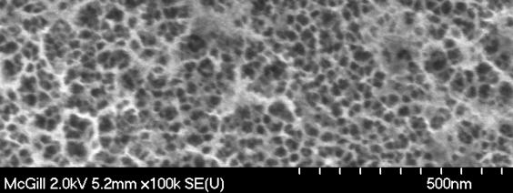
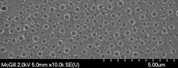
61 Issues & Iomplications Transport properties are function of confinement length (e.g. in quantum wells) because of the change in the Density of States Relative strength of each scattering different from bulk Electrons tend to stay away from the interface as wave function vanishes near the interface
62 Nanostructures Density of States
63 Issues & Implications Effective resistance (ballistic & effects of splitting energy level) Conductance is quantized and has a maximum value for a channel with one level 1 nq 2 τ = = σ ρ m dp = dt G = mv 2 τ q h 2 Familiar voltage divider and current divider rule may not be valid on submicron scales
64 Issues & Implications Validity of effective mass approximation Doping and effects in nanostructures Surface Effects Recombination Hot Carrier Effects Coulomb Blockade
65 Issues & Implications (Looking at nanotechnology from different Angle) Societal Ethical Environmental Health and safety Security Legal and public implications
66 Research Programs in ECE At present there are: 6 PhD 4 M.A.Sc On going researches: 4 major projects Nanodevices based on nanowires Nanodevices based on nanoparticles Optical Sensors, Materials Health Monitoring Investigation on principle issues related to the nanodevices
67 GIS; Device Schematic Electron avalanche current Au nanowires Counter electrode Gas vents Ag/Ti coated Si substrate Negative corona / Field-Emission current Positive corona / Field-Ion current


68 Nanowires Super tips Tubular Structures Nanowhiskers


69 2μm Figure 18. Silver gold alloy nanowires, fabricated by electrochemical deposition for 80 minutes in a modified AAO (with polystyrene microspheres), I=2mA (L= 4μm). 69
).")


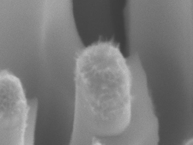
70 Results and Discussion The mentioned textured silicon was electrochemically etched using the same anodization conditions as sampl#7 (I=85mA, t=30min (all conditions are kept constant)). Figure 22-a: Cross section of pyramidal PS fabricated on Si surface of high-concentration hillocks-sample#10. Silicon nano-rods were fabricated on the tip of the pyramidal porous silicon structure with diameter of 200nm and length of 800nm. Figure 22-b: Cross section of one pyramid from sample#10. This image is representing a silicon nano-rod. This structure is of potential for photovoltaic applications. The nano-rods with sharp tips can be also used as AFM probes. 70
71 ENose d Gas Sample (odor) Grid of Sensors Preprocessor Analysis & Control System Pattern Recognition System R. B. Sadeghian & M. Kahrizi, pending patent, 2007

")
72 Biomedical Sensors Devices based on EOT (Extraordinary Optical Transmission) phenomena
 30 25 Spectrophotometry Intensity (counts/sec) 20")
 B On DCDR substrate Experimental condition")

73 Biomedical Sensors (SPR devices) On 5 nm Au network Experimental condition Filter : D1 (reduces the incident radion by 10 times) Spectrophotometry Intensity (counts/sec) ,2 1,0 0,8 0,6 0,4 0, A On DCDR substrate Experimental condition Filter : D1 (reduces the incident radion by 10 times) B On DCDR substrate Experimental condition Filter : No filter C Wavenumber (cm -1 ) A. R. Hajiabol & M.Kahrizi, CSTC 2007 Comparing the Raman intensity to the toxin on DCDR substrate (commercially available)
74 Results Biomolecular Interactions cont d Spectra corresponding to the protein-antibody interaction: Observed A) spectrum shift of of the +10 functionalized nm when antibody substrate adsorbed using Au that After was prepared protein adsorption in the lab no B) additional spectrum shift of the but antibody observed shoulder adsorbed around on the 600 substrate nm C) spectrum of the previously absorbed antibody followed by the adsorption of the protein on the substrate 74
75 UV-VIS SPECTRUM OF ADDLs ON GOLD A Wavelength (nm)
76 Subjects to be covered: Quantum Mechanics & Nanostructures (a brief introduction to the principles of QM, followed by discussion on issues related to nanostructures) Nanostructures (in this section we discuss fabrications and characterizations of nanoparticles, nanowires, thin films, quantum dots, and carbon nanotubes.) Physical phenomena in nano-scale structures (we discuss self-assembly, plasmonic effects, ) Applications of nanotechnology (physical, mechanical, chemical, biological, medical, applications will be presented) Nanotechnology and societal implications (issues like health, safety, security, environmental, will be discussed) Course projects (the projects presented by students in the class are complimentary to the materials covered in the class
An Introduction to NanoScience and NanoTechnology
 An Introduction to NanoScience and NanoTechnology ELEC 6271 An Overview Introduction Evolution of IC characteristics in order of magnitude from the time that the technology was introduced in 1960: In 1960
Seminars in Nanosystems - I
 Seminars in Nanosystems - I Winter Semester 2011/2012 Dr. Emanuela Margapoti Emanuela.Margapoti@wsi.tum.de Dr. Gregor Koblmüller Gregor.Koblmueller@wsi.tum.de Seminar Room at ZNN 1 floor Topics of the
Nanostructures. Lecture 13 OUTLINE
 Nanostructures MTX9100 Nanomaterials Lecture 13 OUTLINE -What is quantum confinement? - How can zero-dimensional materials be used? -What are one dimensional structures? -Why does graphene attract so much
29: Nanotechnology. What is Nanotechnology? Properties Control and Understanding. Nanomaterials
 29: Nanotechnology What is Nanotechnology? Properties Control and Understanding Nanomaterials Making nanomaterials Seeing at the nanoscale Quantum Dots Carbon Nanotubes Biology at the Nanoscale Some Applications
In the name of Allah
 In the name of Allah Nano chemistry- 4 th stage Lecture No. 1 History of nanotechnology 16-10-2016 Assistance prof. Dr. Luma Majeed Ahmed lumamajeed2013@gmail.com, luma.ahmed@uokerbala.edu.iq Nano chemistry-4
Nanotechnology. Yung Liou P601 Institute of Physics Academia Sinica
 Nanotechnology Yung Liou P601 yung@phys.sinica.edu.tw Institute of Physics Academia Sinica 1 1st week Definition of Nanotechnology The Interagency Subcommittee on Nanoscale Science, Engineering and Technology
EN2912C: Future Directions in Computing Lecture 08: Overview of Near-Term Emerging Computing Technologies
 EN2912C: Future Directions in Computing Lecture 08: Overview of Near-Term Emerging Computing Technologies Prof. Sherief Reda Division of Engineering Brown University Fall 2008 1 Near-term emerging computing
In today s lecture, we will cover:
 In today s lecture, we will cover: Metal and Metal oxide Nanoparticles Semiconductor Nanocrystals Carbon Nanotubes 1 Week 2: Nanoparticles Goals for this section Develop an understanding of the physical
Electrical and Optical Properties. H.Hofmann
 Introduction to Nanomaterials Electrical and Optical Properties H.Hofmann Electrical Properties Ohm: G= σw/l where is the length of the conductor, measured in meters [m], A is the cross-section area of
Nanotechnology Fabrication Methods.
 Nanotechnology Fabrication Methods. 10 / 05 / 2016 1 Summary: 1.Introduction to Nanotechnology:...3 2.Nanotechnology Fabrication Methods:...5 2.1.Top-down Methods:...7 2.2.Bottom-up Methods:...16 3.Conclusions:...19
Nanoelectronics. Topics
 Nanoelectronics Topics Moore s Law Inorganic nanoelectronic devices Resonant tunneling Quantum dots Single electron transistors Motivation for molecular electronics The review article Overview of Nanoelectronic
Quantum Dots for Advanced Research and Devices
 Quantum Dots for Advanced Research and Devices spectral region from 450 to 630 nm Zero-D Perovskite Emit light at 520 nm ABOUT QUANTUM SOLUTIONS QUANTUM SOLUTIONS company is an expert in the synthesis
Fabrication at the nanoscale for nanophotonics
 Fabrication at the nanoscale for nanophotonics Ilya Sychugov, KTH Materials Physics, Kista silicon nanocrystal by electron beam induced deposition lithography Outline of basic nanofabrication methods Devices
Nanophysics: Main trends
 Nano-opto-electronics Nanophysics: Main trends Nanomechanics Main issues Light interaction with small structures Molecules Nanoparticles (semiconductor and metallic) Microparticles Photonic crystals Nanoplasmonics
Chapter 10. Nanometrology. Oxford University Press All rights reserved.
 Chapter 10 Nanometrology Oxford University Press 2013. All rights reserved. 1 Introduction Nanometrology is the science of measurement at the nanoscale level. Figure illustrates where nanoscale stands
There's Plenty of Room at the Bottom
 There's Plenty of Room at the Bottom 12/29/1959 Feynman asked why not put the entire Encyclopedia Britannica (24 volumes) on a pin head (requires atomic scale recording). He proposed to use electron microscope
materials, devices and systems through manipulation of matter at nanometer scale and exploitation of novel phenomena which arise because of the
 Nanotechnology is the creation of USEFUL/FUNCTIONAL materials, devices and systems through manipulation of matter at nanometer scale and exploitation of novel phenomena which arise because of the nanometer
1. Introduction : 1.2 New properties:
 Nanodevices In Electronics Rakesh Kasaraneni(PID : 4672248) Department of Electrical Engineering EEL 5425 Introduction to Nanotechnology Florida International University Abstract : This paper describes
Fabrication Methods: Chapter 4. Often two methods are typical. Top Down Bottom up. Begins with atoms or molecules. Begins with bulk materials
 Fabrication Methods: Chapter 4 Often two methods are typical Top Down Bottom up Begins with bulk materials Begins with atoms or molecules Reduced in size to nano By thermal, physical Chemical, electrochemical
ESH Benign Processes for he Integration of Quantum Dots (QDs)
") ESH Benign Processes for he Integration of Quantum Dots (QDs) PIs: Karen K. Gleason, Department of Chemical Engineering, MIT Graduate Students: Chia-Hua Lee: PhD Candidate, Department of Material Science
ESH Benign Processes for he Integration of Quantum Dots (QDs) PIs: Karen K. Gleason, Department of Chemical Engineering, MIT Graduate Students: Chia-Hua Lee: PhD Candidate, Department of Material Science
Self-study problems and questions Processing and Device Technology, FFF110/FYSD13
 Self-study problems and questions Processing and Device Technology, FFF110/FYSD13 Version 2016_01 In addition to the problems discussed at the seminars and at the lectures, you can use this set of problems
Nanostrukturphysik (Nanostructure Physics)
") Nanostrukturphysik (Nanostructure Physics) Prof. Yong Lei & Dr. Yang Xu Fachgebiet 3D-Nanostrukturierung, Institut für Physik Contact: yong.lei@tu-ilmenau.de; yang.xu@tu-ilmenau.de Office: Unterpoerlitzer
Nanostrukturphysik (Nanostructure Physics) Prof. Yong Lei & Dr. Yang Xu Fachgebiet 3D-Nanostrukturierung, Institut für Physik Contact: yong.lei@tu-ilmenau.de; yang.xu@tu-ilmenau.de Office: Unterpoerlitzer
Graphene and Carbon Nanotubes
 Graphene and Carbon Nanotubes 1 atom thick films of graphite atomic chicken wire Novoselov et al - Science 306, 666 (004) 100μm Geim s group at Manchester Novoselov et al - Nature 438, 197 (005) Kim-Stormer
From nanophysics research labs to cell phones. Dr. András Halbritter Department of Physics associate professor
 From nanophysics research labs to cell phones Dr. András Halbritter Department of Physics associate professor Curriculum Vitae Birth: 1976. High-school graduation: 1994. Master degree: 1999. PhD: 2003.
ME 4875/MTE C16. Introduction to Nanomaterials and Nanotechnology. Lecture 2 - Applications of Nanomaterials + Projects
 ME 4875/MTE 575 - C16 Introduction to Nanomaterials and Nanotechnology Lecture 2 - Applications of Nanomaterials + Projects 1 Project Teams of 4 students each Literature review of one application of nanotechnology
Nanomaterials and their Optical Applications
 Nanomaterials and their Optical Applications Winter Semester 2013 Lecture 02 rachel.grange@uni-jena.de http://www.iap.uni-jena.de/multiphoton Lecture 2: outline 2 Introduction to Nanophotonics Theoretical
TECHNICAL INFORMATION. Quantum Dot
 Quantum Dot Quantum Dot is the nano meter sized semiconductor crystal with specific optical properties originates from the phenomenon which can be explained by the quantum chemistry and quantum mechanics.
Nano-mechatronics. Presented by: György BudaváriSzabó (X0LY4M)
") Nano-mechatronics Presented by: György BudaváriSzabó (X0LY4M) Nano-mechatronics Nano-mechatronics is currently used in broader spectra, ranging from basic applications in robotics, actuators, sensors,
Nano-mechatronics Presented by: György BudaváriSzabó (X0LY4M) Nano-mechatronics Nano-mechatronics is currently used in broader spectra, ranging from basic applications in robotics, actuators, sensors,
There s plenty of room at the bottom! - R.P. Feynman, Nanostructure: a piece of material with at least one dimension less than 100 nm in extent.
 Nanostructures and Nanotechnology There s plenty of room at the bottom! - R.P. Feynman, 1959 Materials behave differently when structured at the nm scale than they do in bulk. Technologies now exist that
RAJASTHAN TECHNICAL UNIVERSITY, KOTA
 RAJASTHAN TECHNICAL UNIVERSITY, KOTA (Electronics & Communication) Submitted By: LAKSHIKA SOMANI E&C II yr, IV sem. Session: 2007-08 Department of Electronics & Communication Geetanjali Institute of Technical
Graphene Fundamentals and Emergent Applications
 Graphene Fundamentals and Emergent Applications Jamie H. Warner Department of Materials University of Oxford Oxford, UK Franziska Schaffel Department of Materials University of Oxford Oxford, UK Alicja
Chapter 12. Nanometrology. Oxford University Press All rights reserved.
 Chapter 12 Nanometrology Introduction Nanometrology is the science of measurement at the nanoscale level. Figure illustrates where nanoscale stands in relation to a meter and sub divisions of meter. Nanometrology
Nanoparticles, nanorods, nanowires
 Nanoparticles, nanorods, nanowires Nanoparticles, nanocrystals, nanospheres, quantum dots, etc. Drugs, proteins, etc. Nanorods, nanowires. Optical and electronic properties. Organization using biomolecules.
Nanotechnology. Gavin Lawes Department of Physics and Astronomy
 Nanotechnology Gavin Lawes Department of Physics and Astronomy Earth-Moon distance 4x10 8 m (courtesy NASA) Length scales (Part I) Person 2m Magnetic nanoparticle 5x10⁻⁹ m 10 10 m 10 5 m 1 m 10-5 m 10-10
The first three categories are considered a bottom-up approach while lithography is a topdown
 Nanowires and Nanorods One-dimensional structures have been called in different ways: nanowires, nanorod, fibers of fibrils, whiskers, etc. The common characteristic of these structures is that all they
Carbon Nanomaterials: Nanotubes and Nanobuds and Graphene towards new products 2030
 Carbon Nanomaterials: Nanotubes and Nanobuds and Graphene towards new products 2030 Prof. Dr. Esko I. Kauppinen Helsinki University of Technology (TKK) Espoo, Finland Forecast Seminar February 13, 2009
Wafer-scale fabrication of graphene
 Wafer-scale fabrication of graphene Sten Vollebregt, MSc Delft University of Technology, Delft Institute of Mircosystems and Nanotechnology Delft University of Technology Challenge the future Delft University
Nanostrukturphysik (Nanostructure Physics)
") Nanostrukturphysik (Nanostructure Physics) Prof. Yong Lei & Dr. Yang Xu Fachgebiet 3D-Nanostrukturierung, Institut für Physik Contact: yong.lei@tu-ilmenau.de; yang.xu@tu-ilmenau.de Office: Unterpoerlitzer
Nanostrukturphysik (Nanostructure Physics) Prof. Yong Lei & Dr. Yang Xu Fachgebiet 3D-Nanostrukturierung, Institut für Physik Contact: yong.lei@tu-ilmenau.de; yang.xu@tu-ilmenau.de Office: Unterpoerlitzer
Introduction to Nanotechnology Chapter 5 Carbon Nanostructures Lecture 1
 Introduction to Nanotechnology Chapter 5 Carbon Nanostructures Lecture 1 ChiiDong Chen Institute of Physics, Academia Sinica chiidong@phys.sinica.edu.tw 02 27896766 Carbon contains 6 electrons: (1s) 2,
CHAPTER 11 Semiconductor Theory and Devices
 CHAPTER 11 Semiconductor Theory and Devices 11.1 Band Theory of Solids 11.2 Semiconductor Theory 11.3 Semiconductor Devices 11.4 Nanotechnology It is evident that many years of research by a great many
Introduction to Nanotechnology Chapter 5 Carbon Nanostructures Lecture 1
 Introduction to Nanotechnology Chapter 5 Carbon Nanostructures Lecture 1 ChiiDong Chen Institute of Physics, Academia Sinica chiidong@phys.sinica.edu.tw 02 27896766 Section 5.2.1 Nature of the Carbon Bond
Fabrication / Synthesis Techniques
 Quantum Dots Physical properties Fabrication / Synthesis Techniques Applications Handbook of Nanoscience, Engineering, and Technology Ch.13.3 L. Kouwenhoven and C. Marcus, Physics World, June 1998, p.35
Graphene. Tianyu Ye November 30th, 2011
 Graphene Tianyu Ye November 30th, 2011 Outline What is graphene? How to make graphene? (Exfoliation, Epitaxial, CVD) Is it graphene? (Identification methods) Transport properties; Other properties; Applications;
Chapter 3 Properties of Nanostructures
 Chapter 3 Properties of Nanostructures In Chapter 2, the reduction of the extent of a solid in one or more dimensions was shown to lead to a dramatic alteration of the overall behavior of the solids. Generally,
Top down and bottom up fabrication
 Lecture 24 Top down and bottom up fabrication Lithography ( lithos stone / graphein to write) City of words lithograph h (Vito Acconci, 1999) 1930 s lithography press Photolithography d 2( NA) NA=numerical
Lecture 6: Individual nanoparticles, nanocrystals and quantum dots
 Lecture 6: Individual nanoparticles, nanocrystals and quantum dots Definition of nanoparticle: Size definition arbitrary More interesting: definition based on change in physical properties. Size smaller
Halbleiter. Prof. Yong Lei. Prof. Thomas Hannappel.
 Halbleiter Prof. Yong Lei Prof. Thomas Hannappel yong.lei@tu-ilemnau.de thomas.hannappel@tu-ilmenau.de Important Events in Semiconductors History 1833 Michael Faraday discovered temperature-dependent conductivity
2D Materials for Gas Sensing
 2D Materials for Gas Sensing S. Guo, A. Rani, and M.E. Zaghloul Department of Electrical and Computer Engineering The George Washington University, Washington DC 20052 Outline Background Structures of
Contents. Preface to the first edition
 Contents List of authors Preface to the first edition Introduction x xi xiii 1 The nanotechnology revolution 1 1.1 From micro- to nanoelectronics 2 1.2 From the macroscopic to the nanoscopic world 4 1.3
NANO TECHNOLOGY IN POLYMER SOLAR CELLS. Mayur Padharia, Hardik Panchal, Keval Shah, *Neha Patni, Shibu.G.Pillai
 NANO TECHNOLOGY IN POLYMER SOLAR CELLS Mayur Padharia, Hardik Panchal, Keval Shah, *Neha Patni, Shibu.G.Pillai Department of Chemical Engineering, Institute of Technology, Nirma University, S. G. Highway,
Carbon based Nanoscale Electronics
 Carbon based Nanoscale Electronics 09 02 200802 2008 ME class Outline driving force for the carbon nanomaterial electronic properties of fullerene exploration of electronic carbon nanotube gold rush of
Semiconductor Nanowires: Motivation
 Semiconductor Nanowires: Motivation Patterning into sub 50 nm range is difficult with optical lithography. Self-organized growth of nanowires enables 2D confinement of carriers with large splitting of
Device 3D. 3D Device Simulator. Nano Scale Devices. Fin FET
 Device 3D 3D Device Simulator Device 3D is a physics based 3D device simulator for any device type and includes material properties for the commonly used semiconductor materials in use today. The physical
Kavli Workshop for Journalists. June 13th, CNF Cleanroom Activities
 Kavli Workshop for Journalists June 13th, 2007 CNF Cleanroom Activities Seeing nm-sized Objects with an SEM Lab experience: Scanning Electron Microscopy Equipment: Zeiss Supra 55VP Scanning electron microscopes
Electrochemically Synthesized Multi-block
 Electrochemically Synthesized Multi-block Nanorods Sungho Park SungKyunKwan University, Department of Chemistry & SKKU Advanced Institute of Nanotechnology (SAINT) J. Am. Chem. Soc. 2003, 125, 2282-2290
Forming Gradient Multilayer (GML) Nano Films for Photovoltaic and Energy Storage Applications
 Nano Films for Photovoltaic and Energy Storage Applications") Forming Gradient Multilayer (GML) Nano Films for Photovoltaic and Energy Storage Applications ABSTRACT Boris Gilman and Igor Altman Coolsol R&C, Mountain View CA For successful implementation of the nanomaterial-based
Forming Gradient Multilayer (GML) Nano Films for Photovoltaic and Energy Storage Applications ABSTRACT Boris Gilman and Igor Altman Coolsol R&C, Mountain View CA For successful implementation of the nanomaterial-based
CHAPTER 3. OPTICAL STUDIES ON SnS NANOPARTICLES
 42 CHAPTER 3 OPTICAL STUDIES ON SnS NANOPARTICLES 3.1 INTRODUCTION In recent years, considerable interest has been shown on semiconducting nanostructures owing to their enhanced optical and electrical
Physics and Material Science of Semiconductor Nanostructures
 Physics and Material Science of Semiconductor Nanostructures PHYS 570P Prof. Oana Malis Email: omalis@purdue.edu Course website: http://www.physics.purdue.edu/academic_programs/courses/phys570p/ 1 Course
Supporting Information
 Supporting Information Superstructural Raman Nanosensors with Integrated Dual Functions for Ultrasensitive Detection and Tunable Release of Molecules Jing Liu #, Jianhe Guo #, Guowen Meng and Donglei Fan*
Carbon nanotubes in a nutshell. Graphite band structure. What is a carbon nanotube? Start by considering graphite.
 Carbon nanotubes in a nutshell What is a carbon nanotube? Start by considering graphite. sp 2 bonded carbon. Each atom connected to 3 neighbors w/ 120 degree bond angles. Hybridized π bonding across whole
Materials. Definitions of nanotechnology. The term nanotechnology was invented by Professor Norio Taniguchi at the University of Tokyo in 1971.
 Materials Definitions of nanotechnology The term nanotechnology was invented by Professor Norio Taniguchi at the University of Tokyo in 1971. The original definition, translated into English Nano-technology'
Nanoscale Issues in Materials & Manufacturing
 Nanoscale Issues in Materials & Manufacturing ENGR 213 Principles of Materials Engineering Module 2: Introduction to Nanoscale Issues Top-down and Bottom-up Approaches for Fabrication Winfried Teizer,
OPTI510R: Photonics. Khanh Kieu College of Optical Sciences, University of Arizona Meinel building R.626
 OPTI510R: Photonics Khanh Kieu College of Optical Sciences, University of Arizona kkieu@optics.arizona.edu Meinel building R.626 Announcements HW#3 is assigned due Feb. 20 st Mid-term exam Feb 27, 2PM
Nanomaterial based Environmental Sensing. Sung Ik Yang Kyung Hee University
 Nanomaterial based Environmental Sensing Sung Ik Yang Kyung Hee University What is Nanotechnology? - understanding and control of matter at dimensions less than 100 nanometers- unique phenomena enable
what happens if we make materials smaller?
 what happens if we make materials smaller? IAP VI/10 ummer chool 2007 Couvin Prof. ns outline Introduction making materials smaller? ynthesis how do you make nanomaterials? Properties why would you make
Overview. Carbon in all its forms. Background & Discovery Fabrication. Important properties. Summary & References. Overview of current research
 Graphene Prepared for Solid State Physics II Pr Dagotto Spring 2009 Laurene Tetard 03/23/09 Overview Carbon in all its forms Background & Discovery Fabrication Important properties Overview of current
EE 5344 Introduction to MEMS CHAPTER 5 Radiation Sensors
 EE 5344 Introduction to MEMS CHAPTER 5 Radiation Sensors 5. Radiation Microsensors Radiation µ-sensors convert incident radiant signals into standard electrical out put signals. Radiant Signals Classification
Lecture 1. Introduction to Electronic Materials. Reading: Pierret 1.1, 1.2, 1.4,
 Lecture 1 Introduction to Electronic Materials Reading: Pierret 1.1, 1.2, 1.4, 2.1-2.6 Atoms to Operational Amplifiers The goal of this course is to teach the fundamentals of non-linear circuit elements
High-resolution Characterization of Organic Ultrathin Films Using Atomic Force Microscopy
 High-resolution Characterization of Organic Ultrathin Films Using Atomic Force Microscopy Jing-jiang Yu Nanotechnology Measurements Division Agilent Technologies, Inc. Atomic Force Microscopy High-Resolution
Lecture 0: Introduction
 Lecture 0: Introduction Introduction q Integrated circuits: many transistors on one chip q Very Large Scale Integration (VLSI): bucketloads! q Complementary Metal Oxide Semiconductor Fast, cheap, low power
Instrumentation and Operation
 Instrumentation and Operation 1 STM Instrumentation COMPONENTS sharp metal tip scanning system and control electronics feedback electronics (keeps tunneling current constant) image processing system data
Molecular Electronics For Fun and Profit(?)
") Molecular Electronics For Fun and Profit(?) Prof. Geoffrey Hutchison Department of Chemistry University of Pittsburgh geoffh@pitt.edu July 22, 2009 http://hutchison.chem.pitt.edu Moore s Law: Transistor
Molecular Electronics For Fun and Profit(?) Prof. Geoffrey Hutchison Department of Chemistry University of Pittsburgh geoffh@pitt.edu July 22, 2009 http://hutchison.chem.pitt.edu Moore s Law: Transistor
Dip-Pen Lithography 1
 Dip-Pen Lithography 1 A Brief History of Writing Instruments From Quills and Bamboos to fountain pens and brushes M. Klein and Henry W. Wynne received US patent #68445 in 1867 for an ink chamber and delivery
Chapter 12 - Modern Materials
 Chapter 12 - Modern Materials 12.1 Semiconductors Inorganic compounds that semiconduct tend to have chemical formulas related to Si and Ge valence electron count of four. Semiconductor conductivity can
Carbon Nanomaterials
 Carbon Nanomaterials STM Image 7 nm AFM Image Fullerenes C 60 was established by mass spectrographic analysis by Kroto and Smalley in 1985 C 60 is called a buckminsterfullerene or buckyball due to resemblance
Carbon Nanotube: Property, application and ultrafast optical spectroscopy
 Carbon Nanotube: Property, application and ultrafast optical spectroscopy Yijing Fu 1, Qing Yu 1 Institute of Optics, University of Rochester Department of Electrical engineering, University of Rochester
Chapter 1 Overview of Semiconductor Materials and Physics
 Chapter 1 Overview of Semiconductor Materials and Physics Professor Paul K. Chu Conductivity / Resistivity of Insulators, Semiconductors, and Conductors Semiconductor Elements Period II III IV V VI 2 B
Nanotechnology where size matters
 Nanotechnology where size matters J Emyr Macdonald Overview Ways of seeing very small things What is nanotechnology and why is it important? Building nanostructures What we can do with nanotechnology?
Nanomaterials Electrical and Optical Properties
 Nanomaterials Electrical and Optical Properties H.Hofmann ÉCOLE POLYTECHNIQUE FÉDÉRALE DE LAUSANNE Electrical Properties Energy LUMO HOMO Forbidden bandgap Atom Mo lecule Cluster Nanoparticle Semi conductor
Metallic: 2n 1. +n 2. =3q Armchair structure always metallic = 2
 Properties of CNT d = 2.46 n 2 2 1 + n1n2 + n2 2π Metallic: 2n 1 +n 2 =3q Armchair structure always metallic a) Graphite Valence(π) and Conduction(π*) states touch at six points(fermi points) Carbon Nanotube:
Monolayer Semiconductors
 Monolayer Semiconductors Gilbert Arias California State University San Bernardino University of Washington INT REU, 2013 Advisor: Xiaodong Xu (Dated: August 24, 2013) Abstract Silicon may be unable to
Optical Spectroscopies of Thin Films and Interfaces. Dietrich R. T. Zahn Institut für Physik, Technische Universität Chemnitz, Germany
 Optical Spectroscopies of Thin Films and Interfaces Dietrich R. T. Zahn Institut für Physik, Technische Universität Chemnitz, Germany 1. Introduction 2. Vibrational Spectroscopies (Raman and Infrared)
e - Galvanic Cell 1. Voltage Sources 1.1 Polymer Electrolyte Membrane (PEM) Fuel Cell
 Fuel Cell") Galvanic cells convert different forms of energy (chemical fuel, sunlight, mechanical pressure, etc.) into electrical energy and heat. In this lecture, we are interested in some examples of galvanic cells.
Galvanic cells convert different forms of energy (chemical fuel, sunlight, mechanical pressure, etc.) into electrical energy and heat. In this lecture, we are interested in some examples of galvanic cells.
Materials and Structural Design for Advanced Energy Storage Devices
 Materials and Structural Design for Advanced Energy Storage Devices Imran Shakir Sustainable Energy Technologies Center (SET) King Saud University Saudi Arabia Specific Power (W/kg) Introduction and Motivation
NANOMEDICINE. WILEY A John Wiley and Sons, Ltd., Publication DESIGN AND APPLICATIONS OF MAGNETIC NANOMATERIALS, NANOSENSORS AND NANOSYSTEMS
 NANOMEDICINE DESIGN AND APPLICATIONS OF MAGNETIC NANOMATERIALS, NANOSENSORS AND NANOSYSTEMS Vijay K. Varadan Linfeng Chen Jining Xie WILEY A John Wiley and Sons, Ltd., Publication Preface About the Authors
Semiconductors and Optoelectronics. Today Semiconductors Acoustics. Tomorrow Come to CH325 Exercises Tours
 Semiconductors and Optoelectronics Advanced Physics Lab, PHYS 3600 Don Heiman, Northeastern University, 2017 Today Semiconductors Acoustics Tomorrow Come to CH325 Exercises Tours Semiconductors and Optoelectronics
EV Group. Engineered Substrates for future compound semiconductor devices
 EV Group Engineered Substrates for future compound semiconductor devices Engineered Substrates HB-LED: Engineered growth substrates GaN / GaP layer transfer Mobility enhancement solutions: III-Vs to silicon
Lecture 3: Heterostructures, Quasielectric Fields, and Quantum Structures
 Lecture 3: Heterostructures, Quasielectric Fields, and Quantum Structures MSE 6001, Semiconductor Materials Lectures Fall 2006 3 Semiconductor Heterostructures A semiconductor crystal made out of more
Nanostructure. Materials Growth Characterization Fabrication. More see Waser, chapter 2
 Nanostructure Materials Growth Characterization Fabrication More see Waser, chapter 2 Materials growth - deposition deposition gas solid Physical Vapor Deposition Chemical Vapor Deposition Physical Vapor
Carbon Nanotubes in Interconnect Applications
 Carbon Nanotubes in Interconnect Applications Page 1 What are Carbon Nanotubes? What are they good for? Why are we interested in them? - Interconnects of the future? Comparison of electrical properties
Chapter 3 Engineering Science for Microsystems Design and Fabrication
 Lectures on MEMS and MICROSYSTEMS DESIGN and MANUFACTURE Chapter 3 Engineering Science for Microsystems Design and Fabrication In this Chapter, we will present overviews of the principles of physical and
Quantized Electrical Conductance of Carbon nanotubes(cnts)
") Quantized Electrical Conductance of Carbon nanotubes(cnts) By Boxiao Chen PH 464: Applied Optics Instructor: Andres L arosa Abstract One of the main factors that impacts the efficiency of solar cells is
Quantized Electrical Conductance of Carbon nanotubes(cnts) By Boxiao Chen PH 464: Applied Optics Instructor: Andres L arosa Abstract One of the main factors that impacts the efficiency of solar cells is
Contents. Foreword by Darrell H. Reneker
 Table of Foreword by Darrell H. Reneker Preface page xi xiii 1 Introduction 1 1.1 How big is a nanometer? 1 1.2 What is nanotechnology? 1 1.3 Historical development of nanotechnology 2 1.4 Classification
Nanosphere Lithography
 Nanosphere Lithography Derec Ciafre 1, Lingyun Miao 2, and Keita Oka 1 1 Institute of Optics / 2 ECE Dept. University of Rochester Abstract Nanosphere Lithography is quickly emerging as an efficient, low
Final Reading Assignment: Travels to the Nanoworld: pages pages pages
 Final Reading Assignment: Travels to the Nanoworld: pages 152-164 pages 201-214 pages 219-227 Bottom-up nanofabrication Can we assemble nanomachines manually? What are the components (parts)? nanoparticles
Nanoscale optical circuits: controlling light using localized surface plasmon resonances
 Nanoscale optical circuits: controlling light using localized surface plasmon resonances T. J. Davis, D. E. Gómez and K. C. Vernon CSIRO Materials Science and Engineering Localized surface plasmon (LSP)
ELECTRONIC DEVICES AND CIRCUITS SUMMARY
 ELECTRONIC DEVICES AND CIRCUITS SUMMARY Classification of Materials: Insulator: An insulator is a material that offers a very low level (or negligible) of conductivity when voltage is applied. Eg: Paper,
Appendix A. Assessments Points 4 Mode of Assessments. New Course Code and Title Course Coordinator. MS741M Nanomaterials
 New Course Code and Title Course Coordinator Details of Course MS741M Nanomaterials AP Jason Xu (Course Coordinator) AP Xue Can Rationale for introducing this course This course will cover the subject
Nanobiotechnology. Place: IOP 1 st Meeting Room Time: 9:30-12:00. Reference: Review Papers. Grade: 40% midterm, 60% final report (oral + written)
") Nanobiotechnology Place: IOP 1 st Meeting Room Time: 9:30-12:00 Reference: Review Papers Grade: 40% midterm, 60% final report (oral + written) Midterm: 5/18 Oral Presentation 1. 20 minutes each person
Nanobiotechnology Place: IOP 1 st Meeting Room Time: 9:30-12:00 Reference: Review Papers Grade: 40% midterm, 60% final report (oral + written) Midterm: 5/18 Oral Presentation 1. 20 minutes each person
Introduction to semiconductor nanostructures. Peter Kratzer Modern Concepts in Theoretical Physics: Part II Lecture Notes
 Introduction to semiconductor nanostructures Peter Kratzer Modern Concepts in Theoretical Physics: Part II Lecture Notes What is a semiconductor? The Fermi level (chemical potential of the electrons) falls