Lecture 1. Introduction to Electronic Materials. Reading: Pierret 1.1, 1.2, 1.4,
|
|
|
- Loraine Miles
- 6 years ago
- Views:
Transcription
1 Lecture 1 Introduction to Electronic Materials Reading: Pierret 1.1, 1.2, 1.4,
2 Atoms to Operational Amplifiers The goal of this course is to teach the fundamentals of non-linear circuit elements including diodes, and transistors (BJT and FET), how they are used in circuits and real world applications. The course takes an atoms to opamps approach in which you learn about the fundamentals of electron movement in semiconductor materials and develop this basic knowledge into how we can construct devices from these materials that can control the flow of electrons in useful ways. We then extend this knowledge to how these devices can be used to form circuits that perform useful functions on electrical signals.

3 ... Atoms to Everything Else in Optoelectronics The goal of this course is to teach the fundamentals of non-linear circuit elements including diodes, and transistors (BJT and FET), how they are used in circuits and real world applications. The course takes an atoms to opamps approach in which you learn about the fundamentals of electron movement in semiconductor materials and develop this basic knowledge into how we can construct devices from these materials that can control the flow of electrons in useful ways. We then extend this knowledge to how these devices can be used to form circuits that perform useful functions on electrical signals. Nakamura, S. et al., High-power InGaN single-quantum-well-structure blue and violet light-emitting diodes, Appl. Phys. Lett 67, 1868 (1995).

4 Modern amplifiers consist of extremely small devices Transistors in the above image are only a few microns ( m or 1e-6 meters) on a side. Modern devices have lateral dimensions that are only fractions of a micron (~0.1 m) and vertical dimensions that may be only a few atoms tall.
5 Control of Conductivity is the Key to Modern Electronic Devices Conductivity,, is the ease with which a given material conducts electricity. Ohms Law: V=IR or J= E where J is current density and E is electric field. Metals: High conductivity Insulators: Low Conductivity Semiconductors: Conductivity can be varied by several orders of magnitude. It is the ability to control conductivity that make semiconductors useful as current/voltage control elements. Current/Voltage control is the key to switches (digital logic including microprocessors etc ), amplifiers, LEDs, LASERs, photodetectors, etc...
6 Classifications of Electronic Materials Example: Silicon n=1 (2 s), n=2 (2 s and 6 p) and n=3 (2 s and 2 p with 4 unoccupied p states) Atoms contain various orbitals, levels or shells of electrons labeled as n=1, 2, 3, 4, etc or K, L, M, or N etc The individual allowed electrons states are simply allowed positions (energy and space) within each orbital/level/shell for which an electron can occupy. Electrons fill up the levels (fill in the individual states in the levels) from the smallest n shell to the largest occupying states (available orbitals) until that orbital is completely filled then going on to the next higher orbital. The outer most orbital/level/shell is called the Valence orbital. This valence orbital si the only one that participated in the bonding of atoms together to form solids.
7 Classifications of Electronic Materials The areas around these identical atoms are equally charged For metals, the electrons can jump from the valence orbits (outermost core energy levels of the atom) to any position within the crystal (free to move throughout the crystal) with no extra energy needed to be supplied For insulators, it is VERY DIFFICULT for the electrons to jump from the valence orbits and requires a huge amount of energy to free the electron from the atomic core. For semiconductors, the electrons can jump from the valence orbits but does require a small amount of energy to free the electron from the atomic core.
8 Classifications of Electronic Materials For metals, the electrons can jump from the valence orbits (outermost core energy levels of the atom) to any position within the crystal (free to move throughout the crystal) with no extra energy needed to be supplied For insulators, it is VERY DIFFICULT for the electrons to jump from the valence orbits and requires a huge amount of energy to free the electron from the atomic core. For semiconductors, the electrons can jump from the valence orbits but does require a small amount of energy to free the electron from the atomic core.
9 Classifications of Electronic Materials Valence Electrons Valence electrons can gain energy (thermal, electrical, magnetic or optical energy) and break away from the crystal. New Hole created (empty valence state) that can also move Conduction Electrons (free to move throughout the crystal) Semiconductor materials are a sub-class of materials distinguished by the existence of a range of disallowed energies between the energies of the valence electrons (outermost core electrons) and the energies of electrons free to move throughout the material. The energy difference (energy gap or bandgap) between the states in which the electron is bound to the atom and when it is free to conduct throughout the crystal is related to the bonding strength of the material, it s density, the degree of ionicity of the bond, and the chemistry related to the valence of bonding. High bond strength materials (diamond, SiC, AlN, GaN etc...) tend to have large energy bandgaps. Lower bond strength materials (Si, Ge, etc...) tend to have smaller energy bandgaps.


10 Example: Solar Cells Why do the electrons flow when light is present but not flow when light is not present? Answer, Energy Bandgap (very important concept).
11 Classifications of Electronic Materials More formally, the energy gap is derived from the Pauli exclusion principle, where no two electrons occupying the same space, can have the same energy. Thus, as atoms are brought closer towards one another and begin to bond together, their energy levels must split into bands of discrete levels so closely spaced in energy, they can be considered a continuum of allowed energy. Strongly bonded materials tend to have small interatomic distances between atoms. Thus, the strongly bonded materials can have larger energy bandgaps than do weakly bonded materials.


12 Material Classifications based on Bonding Method Bonds can be classified as metallic, Ionic, Covalent, and van der Waals.
13 Consider the case of the group 4 elements, all** covalently bonded Element Atomic Radius/Lattice Constant Bandgap (How closely spaced are the atoms?) C 0.91/3.56 Angstroms 5.47 ev Si 1.46/5.43 Angstroms 1.12 ev Ge 1.52/5.65 Angstroms 0.66 ev -Sn 1.72/6.49 Angstroms ~0.08 ev* Pb 1.81/** Angstroms Metal *Only has a measurable bandgap near 0K **Different bonding/crystal Structure due to unfilled higher orbital states
14 Classifications of Electronic Materials Types of Semiconductors: Elemental: Silicon or Germanium (Si or Ge) Compound: Gallium Arsenide (GaAs), Indium Phosphide (InP), Silicon Carbide (SiC), CdS and many others Note that the sum of the valence adds to 8, a complete outer shell. I.E. 4+4, 3+5, 2+6, etc...
15 Compound Semiconductors: Offer high performance (optical characteristics, higher frequency, higher power) than elemental semiconductors and greater device design flexibility due to mixing of materials. Binary: GaAs, SiC, etc... Classifications of Electronic Materials Ternary: Al x Ga 1-x As, In x Ga 1-x N where 0<=x<=1 Quaternary: In x Ga 1-x As y P 1-y where 0<=x<=1 and 0<=y<=1 Half the total number of atoms must come from group III (Column III) and the other half the atoms must come from group V (Column V) (or more precisely, IV/IV, III/V, or II/VI combinations) leading to the above reduced semiconductor notation. Example: Assume a compound semiconductor has 25% atomic concentrations of Ga, 25% atomic In and 50% atomic of N. The chemical formula would be: Ga 0.25 In 0.25 N 0.5 But the correct reduced semiconductor formula would be: Ga 0.5 In 0.5 N
, amorphous-si, silicon nitride (Si 3 N 4 ), and others.")
16 Classifications of Electronic Materials Material Classifications based on Crystal Structure Amorphous Materials No discernible long range atomic order (no detectable crystal structure). Examples are silicon dioxide (SiO 2 ), amorphous-si, silicon nitride (Si 3 N 4 ), and others. Though usually thought of as less perfect than crystalline materials, this class of materials is extremely useful. Polycrystalline Materials Material consisting of several domains of crystalline material. Each domain can be oriented differently than other domains. However, within a single domain, the material is crystalline. The size of the domains may range from cubic nanometers to several cubic centimeters. Many semiconductors are polycrystalline as are most metals. Crystalline Materials Crystalline materials are characterized by an atomic symmetry that repeats spatially. The shape of the unit cell depends on the bonding of the material. The most common unit cell structures are diamond, zincblende (a derivative of the diamond structure), hexagonal, and rock salt (simple cubic).


17 Crystalline Order Water Molecules, H 2 O, forming Snowflakes Atoms forming a Semiconductor Need two volunteers (demo on how a crystal forms naturally due to repulsive electronic bonds)

.")
18 Crystal Growth: How do we get Single Crystalline Material? The vast majority of crystalline silicon produced is grown by the Czochralski growth method. In this method, a single crystal seed wafer is brought into contact with a liquid Silicon charge held in a crucible (typically SiO 2 but may have a lining of silicon-nitride or other material). The seed is pulled out of the melt, allowing Si to solidify. The solidified material bonds to the seed crystal in the same atomic pattern as the seed crystal.
19 How do we create Bandgap Engineered Structures? Epitaxy Repeating a crystalline structure by the atom by atom addition. Chemistry controls the epitaxy to insure that, for example, Ga bonds only to N and not Ga-Ga or N-N bonds*.
20 How do we create Bandgap Engineered Structures? Epitaxy
21 How do we create Bandgap Engineered Structures? Epitaxy
22 How do we create Bandgap Engineered Structures? Epitaxy
23 How do we create Bandgap Engineered Structures? Epitaxy
24 How do we create Bandgap Engineered Structures? Epitaxy
25 How do we create Bandgap Engineered Structures? Epitaxy
26 How do we create Bandgap Engineered Structures? Epitaxy
27 How do we create Bandgap Engineered Structures? Epitaxy

28 How do we create Bandgap Engineered Structures? Epitaxy

29 How do we create Bandgap Engineered Structures? Epitaxy
30 How do we create Bandgap Engineered Structures? Epitaxy
31 How do we create Bandgap Engineered Structures? Epitaxy E c E v GaN AlGaN AlGaN AlN GaN GaN GaN GaN


 Shutter")
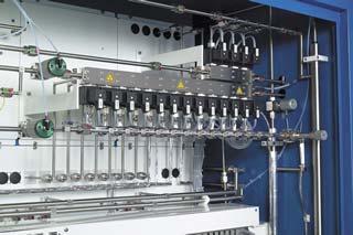
32 MBE Partially disassembled MBE system for clarity RHEED Gun Effusion Furnaces Gas Source (oxygen) Shutter mechanism
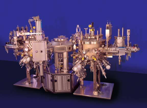
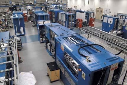
33 Commercial Veeco MBE
34 Alternative Methods: MOCVD Primarily used for II-VI, and III-V semiconductors, special metallic oxides and metals. Metal Organic Chemical Vapor Deposition (MOCVD) Many materials that we wish to deposit have very low vapor pressures and thus are difficult to transport via gases. One solution is to chemically attach the metal (Ga, Al, Cu, etc ) to an organic compound that has a very high vapor pressure. Organic compounds often have very high vapor pressure (for example, alcohol has a strong odor). The organic-metal bond is very weak and can be broken via thermal means on wafer, depositing the metal with the high vapor pressure organic being pumped away. Care must be taken to insure little of the organic byproducts are incorporated. Carbon contamination and unintentional Hydrogen incorporation are sometimes a problem. Human Hazard: As the human body absorbs organic compounds very easily, the metal organics are very easily absorbed by humans. Once in the body, the weak metal-organic bond is easily broken, thus, poisoning the body with heavy metals that often can not be easily removed by normal bodily functions. In extreme cases, blood transfusion is the only solution (if caught in time). Luckily, such poisoning is rare as the pyrophoric (flammable in air) nature of most metal organic means the victim is burned severely before he/she can be contaminated.


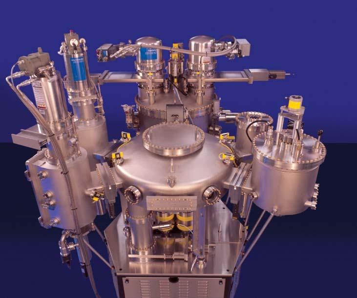
35 Commercial Thomas Swan MOCVD
36 Engineered Energy Behavior in Compound Semiconductors The potential distributions we will use in this class are all possible/common in device structures. Some may represent grown in potentials (quantum wells, etc...) or naturally occurring potentials (parabolic potentials often occur in nature lattice vibrations for example) including periodic potentials such as lattice atoms. E c Kinetic Energy Potential Energy E v E=-qV Arbitrary Reference Energy
37 So much for the introduction. Now on to the meat of the course.
Lecture 2. Unit Cells and Miller Indexes. Reading: (Cont d) Anderson 2 1.8,
 Anderson 2 1.8,") Lecture 2 Unit Cells and Miller Indexes Reading: (Cont d) Anderson 2 1.8, 2.1-2.7 Unit Cell Concept The crystal lattice consists of a periodic array of atoms. Unit Cell Concept A building block that can
Lecture 2 Unit Cells and Miller Indexes Reading: (Cont d) Anderson 2 1.8, 2.1-2.7 Unit Cell Concept The crystal lattice consists of a periodic array of atoms. Unit Cell Concept A building block that can
EECS143 Microfabrication Technology
 EECS143 Microfabrication Technology Professor Ali Javey Introduction to Materials Lecture 1 Evolution of Devices Yesterday s Transistor (1947) Today s Transistor (2006) Why Semiconductors? Conductors e.g
EE143 Fall 2016 Microfabrication Technologies. Evolution of Devices
 EE143 Fall 2016 Microfabrication Technologies Prof. Ming C. Wu wu@eecs.berkeley.edu 511 Sutardja Dai Hall (SDH) 1-1 Evolution of Devices Yesterday s Transistor (1947) Today s Transistor (2006) 1-2 1 Why
Semiconductor Device Physics
 1 Semiconductor Device Physics Lecture 1 http://zitompul.wordpress.com 2 0 1 3 2 Semiconductor Device Physics Textbook: Semiconductor Device Fundamentals, Robert F. Pierret, International Edition, Addison
EE301 Electronics I , Fall
 EE301 Electronics I 2018-2019, Fall 1. Introduction to Microelectronics (1 Week/3 Hrs.) Introduction, Historical Background, Basic Consepts 2. Rewiev of Semiconductors (1 Week/3 Hrs.) Semiconductor materials
A semiconductor is an almost insulating material, in which by contamination (doping) positive or negative charge carriers can be introduced.
 positive or negative charge carriers can be introduced.") Semiconductor A semiconductor is an almost insulating material, in which by contamination (doping) positive or negative charge carriers can be introduced. Page 2 Semiconductor materials Page 3 Energy levels
Semiconductor A semiconductor is an almost insulating material, in which by contamination (doping) positive or negative charge carriers can be introduced. Page 2 Semiconductor materials Page 3 Energy levels
1 Review of semiconductor materials and physics
 Part One Devices 1 Review of semiconductor materials and physics 1.1 Executive summary Semiconductor devices are fabricated using specific materials that offer the desired physical properties. There are
Semiconductor Physics and Devices
 Syllabus Advanced Nano Materials Semiconductor Physics and Devices Textbook Donald A. Neamen (McGraw-Hill) Semiconductor Physics and Devices Seong Jun Kang Department of Advanced Materials Engineering
ELECTRONIC I Lecture 1 Introduction to semiconductor. By Asst. Prof Dr. Jassim K. Hmood
 ELECTRONIC I Lecture 1 Introduction to semiconductor By Asst. Prof Dr. Jassim K. Hmood SOLID-STATE ELECTRONIC MATERIALS Electronic materials generally can be divided into three categories: insulators,
Halbleiter. Prof. Yong Lei. Prof. Thomas Hannappel.
 Halbleiter Prof. Yong Lei Prof. Thomas Hannappel yong.lei@tu-ilemnau.de thomas.hannappel@tu-ilmenau.de Important Events in Semiconductors History 1833 Michael Faraday discovered temperature-dependent conductivity
Ga and P Atoms to Covalent Solid GaP
 Ga and P Atoms to Covalent Solid GaP Band Gaps in Binary Group III-V Semiconductors Mixed Semiconductors Affect of replacing some of the As with P in GaAs Band Gap (ev) (nm) GaAs 1.35 919 (IR) GaP 2.24
ELEC311( 물리전자, Physical Electronics) Course Outlines:
 Course Outlines:") ELEC311( 물리전자, Physical Electronics) Course Outlines: by Professor Jung-Hee Lee Lecture notes are prepared with PPT and available before the class (http://abeek.knu.ac.kr). The topics in the notes are
ELEC311( 물리전자, Physical Electronics) Course Outlines: by Professor Jung-Hee Lee Lecture notes are prepared with PPT and available before the class (http://abeek.knu.ac.kr). The topics in the notes are
EE 346: Semiconductor Devices
 EE 346: Semiconductor Devices Lecture - 5 02/01/2017 Tewodros A. Zewde 1 The One-Electron Atom The potential function is due to the coulomb attraction between the proton and electron and is given by where
Introduction to Semiconductor Physics. Prof.P. Ravindran, Department of Physics, Central University of Tamil Nadu, India
 Introduction to Semiconductor Physics 1 Prof.P. Ravindran, Department of Physics, Central University of Tamil Nadu, India http://folk.uio.no/ravi/cmp2013 Review of Semiconductor Physics Semiconductor fundamentals
EE130: Integrated Circuit Devices
 EE130: Integrated Circuit Devices (online at http://webcast.berkeley.edu) Instructor: Prof. Tsu-Jae King (tking@eecs.berkeley.edu) TA s: Marie Eyoum (meyoum@eecs.berkeley.edu) Alvaro Padilla (apadilla@eecs.berkeley.edu)
Lecture 2 Electrons and Holes in Semiconductors
 EE 471: Transport Phenomena in Solid State Devices Spring 2018 Lecture 2 Electrons and Holes in Semiconductors Bryan Ackland Department of Electrical and Computer Engineering Stevens Institute of Technology
Resistance (R) Temperature (T)
 Temperature (T)") CHAPTER 1 Physical Properties of Elements and Semiconductors 1.1 Introduction Semiconductors constitute a large class of substances which have resistivities lying between those of insulators and conductors.
CHAPTER 1 Physical Properties of Elements and Semiconductors 1.1 Introduction Semiconductors constitute a large class of substances which have resistivities lying between those of insulators and conductors.
Electrons are shared in covalent bonds between atoms of Si. A bound electron has the lowest energy state.
 Photovoltaics Basic Steps the generation of light-generated carriers; the collection of the light-generated carriers to generate a current; the generation of a large voltage across the solar cell; and
Chapter 1 Overview of Semiconductor Materials and Physics
 Chapter 1 Overview of Semiconductor Materials and Physics Professor Paul K. Chu Conductivity / Resistivity of Insulators, Semiconductors, and Conductors Semiconductor Elements Period II III IV V VI 2 B
CHAPTER 2: ENERGY BANDS & CARRIER CONCENTRATION IN THERMAL EQUILIBRIUM. M.N.A. Halif & S.N. Sabki
 CHAPTER 2: ENERGY BANDS & CARRIER CONCENTRATION IN THERMAL EQUILIBRIUM OUTLINE 2.1 INTRODUCTION: 2.1.1 Semiconductor Materials 2.1.2 Basic Crystal Structure 2.1.3 Basic Crystal Growth technique 2.1.4 Valence
OPTI510R: Photonics. Khanh Kieu College of Optical Sciences, University of Arizona Meinel building R.626
 OPTI510R: Photonics Khanh Kieu College of Optical Sciences, University of Arizona kkieu@optics.arizona.edu Meinel building R.626 Announcements HW#3 is assigned due Feb. 20 st Mid-term exam Feb 27, 2PM
Introduction to Engineering Materials ENGR2000. Dr.Coates
 Introduction to Engineering Materials ENGR2000 Chapter 18: Electrical Properties Dr.Coates 18.2 Ohm s Law V = IR where R is the resistance of the material, V is the voltage and I is the current. l R A
Communications with Optical Fibers
 Communications with Optical Fibers In digital communications, signals are generally sent as light pulses along an optical fiber. Information is first converted to an electrical signal in the form of pulses
DO PHYSICS ONLINE ELECTRIC CURRENT FROM IDEAS TO IMPLEMENTATION ATOMS TO TRANSISTORS ELECTRICAL PROPERTIES OF SOLIDS
 DO PHYSICS ONLINE FROM IDEAS TO IMPLEMENTATION 9.4.3 ATOMS TO TRANSISTORS ELECTRICAL PROPERTIES OF SOLIDS ELECTRIC CURRENT Different substances vary considerably in their electrical properties. It is a
Lecture 3b. Bonding Model and Dopants. Reading: (Cont d) Notes and Anderson 2 sections
 Notes and Anderson 2 sections") Lecture 3b Bonding Model and Dopants Reading: (Cont d) Notes and Anderson 2 sections 2.3-2.7 The need for more control over carrier concentration Without help the total number of carriers (electrons and
Lecture 3b Bonding Model and Dopants Reading: (Cont d) Notes and Anderson 2 sections 2.3-2.7 The need for more control over carrier concentration Without help the total number of carriers (electrons and
Semiconductor physics I. The Crystal Structure of Solids
 Lecture 3 Semiconductor physics I The Crystal Structure of Solids 1 Semiconductor materials Types of solids Space lattices Atomic Bonding Imperfection and doping in SOLIDS 2 Semiconductor Semiconductors
EE 5211 Analog Integrated Circuit Design. Hua Tang Fall 2012
 EE 5211 Analog Integrated Circuit Design Hua Tang Fall 2012 Today s topic: 1. Introduction to Analog IC 2. IC Manufacturing (Chapter 2) Introduction What is Integrated Circuit (IC) vs discrete circuits?
Chapter 4: Bonding in Solids and Electronic Properties. Free electron theory
 Chapter 4: Bonding in Solids and Electronic Properties Free electron theory Consider free electrons in a metal an electron gas. regards a metal as a box in which electrons are free to move. assumes nuclei
From Last Time Important new Quantum Mechanical Concepts. Atoms and Molecules. Today. Symmetry. Simple molecules.
 Today From Last Time Important new Quantum Mechanical Concepts Indistinguishability: Symmetries of the wavefunction: Symmetric and Antisymmetric Pauli exclusion principle: only one fermion per state Spin
Week 13 MO Theory, Solids, & metals
 Week 13 MO Theory, Solids, & metals Q UEST IO N 1 Using the molecular orbital energy diagrams below, which one of the following diatomic molecules is LEAST likely to exist? A. Li2 B. Be2 C. B2 D. C2 E.
We have arrived to the question: how do molecular bonds determine the band gap? We have discussed that the silicon atom has four outer electrons.
 ET3034Tux - 2.2.2 - Band Gap 2 - Electrons in Molecular Bonds We have arrived to the question: how do molecular bonds determine the band gap? We have discussed that the silicon atom has four outer electrons.
EECS130 Integrated Circuit Devices
 EECS130 Integrated Circuit Devices Professor Ali Javey 8/30/2007 Semiconductor Fundamentals Lecture 2 Read: Chapters 1 and 2 Last Lecture: Energy Band Diagram Conduction band E c E g Band gap E v Valence
Introduction to Condensed Matter Physics
 Introduction to Condensed Matter Physics Crystalline Solids - Introduction M.P. Vaughan Overview Overview of course Crystal solids Crystal structure Crystal symmetry The reciprocal lattice Band theory
CHAPTER 1 Atoms and bonding. Ionic bonding Covalent bonding Metallic bonding van der Waals bonding
 CHAPTER 1 Atoms and bonding The periodic table Ionic bonding Covalent bonding Metallic bonding van der Waals bonding Atoms and bonding In order to understand the physics of semiconductor (s/c) devices,
Unit IV Semiconductors Engineering Physics
 Introduction A semiconductor is a material that has a resistivity lies between that of a conductor and an insulator. The conductivity of a semiconductor material can be varied under an external electrical
Atoms? All matters on earth made of atoms (made up of elements or combination of elements).
.") Chapter 1 Atoms? All matters on earth made of atoms (made up of elements or combination of elements). Atomic Structure Atom is the smallest particle of an element that can exist in a stable or independent
Chapter 1 Atoms? All matters on earth made of atoms (made up of elements or combination of elements). Atomic Structure Atom is the smallest particle of an element that can exist in a stable or independent
ELECTRONIC DEVICES AND CIRCUITS SUMMARY
 ELECTRONIC DEVICES AND CIRCUITS SUMMARY Classification of Materials: Insulator: An insulator is a material that offers a very low level (or negligible) of conductivity when voltage is applied. Eg: Paper,
Semiconductor Physics and Devices Chapter 3.
 Introduction to the Quantum Theory of Solids We applied quantum mechanics and Schrödinger s equation to determine the behavior of electrons in a potential. Important findings Semiconductor Physics and
DO PHYSICS ONLINE STRUCTURE OF THE ATOM FROM IDEAS TO IMPLEMENTATION ATOMS TO TRANSISTORS STRUCTURE OF ATOMS AND SOLIDS
 DO PHYSIS ONLINE FROM IDEAS TO IMPLEMENTATION 9.4.3 ATOMS TO TRANSISTORS STRUTURE OF ATOMS AND SOLIDS STRUTURE OF THE ATOM In was not until the early 1930 s that scientists had fully developed a model
Semiconductor Polymer
 Semiconductor Polymer Organic Semiconductor for Flexible Electronics Introduction: An organic semiconductor is an organic compound that possesses similar properties to inorganic semiconductors with hole
Bonding in solids The interaction of electrons in neighboring atoms of a solid serves the very important function of holding the crystal together.
 Bonding in solids The interaction of electrons in neighboring atoms of a solid serves the very important function of holding the crystal together. For example Nacl In the Nacl lattice, each Na atom is
Introduction to Electronics and Semiconductor
 Introduction to Electronics and Semiconductor 1 Chapter Objectives To study and understand basic electronics. To study and understand semiconductor principles. 2 Definition Electronics is the branch of
electronics fundamentals
 electronics fundamentals circuits, devices, and applications THOMAS L. FLOYD DAVID M. BUCHLA Lesson 1: Diodes and Applications Semiconductors Figure 1-1 The Bohr model of an atom showing electrons in orbits
Electronic Devices & Circuits
 Electronic Devices & Circuits For Electronics & Communication Engineering By www.thegateacademy.com Syllabus Syllabus for Electronic Devices Energy Bands in Intrinsic and Extrinsic Silicon, Carrier Transport,
ESE370: Circuit-Level Modeling, Design, and Optimization for Digital Systems
 ESE370: Circuit-Level Modeling, Design, and Optimization for Digital Systems Lec 6: September 14, 2015 MOS Model You are Here: Transistor Edition! Previously: simple models (0 and 1 st order) " Comfortable
Physics 156: Applications of Solid State Physics
 Physics 156: Applications of Solid State Physics Instructor: Sue Carter Office NSII 349 Office Hours: Wednesdays 11:30 to 1 pm or by appointment Email: sacarter@ucsc.edu Book: http://ece-www.colorado.edu/~bart/book/book/title.htm
Designing Information Devices and Systems II A. Sahai, J. Roychowdhury, K. Pister Discussion 1A
 EECS 16B Spring 2019 Designing Information Devices and Systems II A. Sahai, J. Roychowdhury, K. Pister Discussion 1A 1 Semiconductor Physics Generally, semiconductors are crystalline solids bonded into
Electronics The basics of semiconductor physics
 Electronics The basics of semiconductor physics Prof. Márta Rencz, Gergely Nagy BME DED September 16, 2013 The basic properties of semiconductors Semiconductors conductance is between that of conductors
Lecture 2. Semiconductor Physics. Sunday 4/10/2015 Semiconductor Physics 1-1
 Lecture 2 Semiconductor Physics Sunday 4/10/2015 Semiconductor Physics 1-1 Outline Intrinsic bond model: electrons and holes Charge carrier generation and recombination Intrinsic semiconductor Doping:
Physics and Material Science of Semiconductor Nanostructures
 Physics and Material Science of Semiconductor Nanostructures PHYS 570P Prof. Oana Malis Email: omalis@purdue.edu Course website: http://www.physics.purdue.edu/academic_programs/courses/phys570p/ 1 Introduction
Solid State Device Fundamentals
 Solid State Device Fundamentals ENS 345 Lecture Course by Alexander M. Zaitsev alexander.zaitsev@csi.cuny.edu Tel: 718 982 2812 Office 4N101b 1 The free electron model of metals The free electron model
Electrons and Molecular Forces
 Electrons and Molecular Forces Chemistry 30 Ms. Hayduk Electron Configuration Atomic Structure Atomic Number Number of protons in the nucleus Defines the element Used to organize the periodic table 1 Bohr
Everything starts with atomic structure and bonding
 Everything starts with atomic structure and bonding not all energy values can be possessed by electrons; e- have discrete energy values we call energy levels or states. The energy values are quantized
Review of Semiconductor Physics. Lecture 3 4 Dr. Tayab Din Memon
 Review of Semiconductor Physics Lecture 3 4 Dr. Tayab Din Memon 1 Electronic Materials The goal of electronic materials is to generate and control the flow of an electrical current. Electronic materials
Polar Bonds and Molecules
 Chemistry 1 of 33 Snow covers approximately 23 percent of Earth s surface. Each individual snowflake is formed from as many as 100 snow crystals. The polar bonds in water molecules influence the distinctive
Electrons in materials. (where are they, what is their energy)
") Electrons in materials (where are they, what is their energy) 1 Lone atoms A single atom has electrons in shells and sub shells. Each of these have a distinct energy level. The diagram shows an example
Electrons in materials (where are they, what is their energy) 1 Lone atoms A single atom has electrons in shells and sub shells. Each of these have a distinct energy level. The diagram shows an example
Calculating Band Structure
 Calculating Band Structure Nearly free electron Assume plane wave solution for electrons Weak potential V(x) Brillouin zone edge Tight binding method Electrons in local atomic states (bound states) Interatomic
Module 6 : PHYSICS OF SEMICONDUCTOR DEVICES Lecture 32 : Bonding in Solids
 Module 6 : PHYSICS OF SEMICONDUCTOR DEVICES Lecture 32 : Bonding in Solids Objectives In this course you will learn the following Bonding in solids. Ionic and covalent bond. Structure of Silicon Concept
Semiconductors and Optoelectronics. Today Semiconductors Acoustics. Tomorrow Come to CH325 Exercises Tours
 Semiconductors and Optoelectronics Advanced Physics Lab, PHYS 3600 Don Heiman, Northeastern University, 2017 Today Semiconductors Acoustics Tomorrow Come to CH325 Exercises Tours Semiconductors and Optoelectronics
Band Gap Engineering. Reading the Periodic Table and Understanding Optical and Electrical Properties in Semiconductors
 The Birnie Group solar class and website were created with much-appreciated support from the NSF CRCD Program under grants 0203504 and 0509886. Continuing Support from the McLaren Endowment is also greatly
Currently, worldwide major semiconductor alloy epitaxial growth is divided into two material groups.
 ICQNM 2014 Currently, worldwide major semiconductor alloy epitaxial growth is divided into two material groups. Cubic: Diamond structures: group IV semiconductors (Si, Ge, C), Cubic zinc-blende structures:
Ionic Bonding. Example: Atomic Radius: Na (r = 0.192nm) Cl (r = 0.099nm) Ionic Radius : Na (r = 0.095nm) Cl (r = 0.181nm)
 Cl (r = 0.099nm) Ionic Radius : Na (r = 0.095nm) Cl (r = 0.181nm)") Ionic Bonding Ion: an atom or molecule that gains or loses electrons (acquires an electrical charge). Atoms form cations (+charge), when they lose electrons, or anions (- charge), when they gain electrons.
Ionic Bonding Ion: an atom or molecule that gains or loses electrons (acquires an electrical charge). Atoms form cations (+charge), when they lose electrons, or anions (- charge), when they gain electrons.
Ch. 2: Energy Bands And Charge Carriers In Semiconductors
 Ch. 2: Energy Bands And Charge Carriers In Semiconductors Discrete energy levels arise from balance of attraction force between electrons and nucleus and repulsion force between electrons each electron
Semiconductors. Semiconductors also can collect and generate photons, so they are important in optoelectronic or photonic applications.
 Semiconductors Semiconducting materials have electrical properties that fall between true conductors, (like metals) which are always highly conducting and insulators (like glass or plastic or common ceramics)
ECE 250 Electronic Devices 1. Electronic Device Modeling
 ECE 250 Electronic Devices 1 ECE 250 Electronic Device Modeling ECE 250 Electronic Devices 2 Introduction to Semiconductor Physics You should really take a semiconductor device physics course. We can only
ESE370: Circuit-Level Modeling, Design, and Optimization for Digital Systems. Today MOS MOS. Capacitor. Idea
 ESE370: Circuit-Level Modeling, Design, and Optimization for Digital Systems Day 9: September 26, 2011 MOS Model Today MOS Structure Basic Idea Semiconductor Physics Metals, insulators Silicon lattice
CLASS 1 & 2 REVISION ON SEMICONDUCTOR PHYSICS. Reference: Electronic Devices by Floyd
 CLASS 1 & 2 REVISION ON SEMICONDUCTOR PHYSICS Reference: Electronic Devices by Floyd 1 ELECTRONIC DEVICES Diodes, transistors and integrated circuits (IC) are typical devices in electronic circuits. All
Bohr s Model, Energy Bands, Electrons and Holes
 Dual Character of Material Particles Experimental physics before 1900 demonstrated that most of the physical phenomena can be explained by Newton's equation of motion of material particles or bodies and
The particles in a solid hold relatively fixed positions.
 Section 3 Solids Key Terms crystalline solid melting crystal structure crystal melting point unit cell amorphous solid supercooled liquid The common expression solid as a rock suggests something that is
From Last Time. Several important conceptual aspects of quantum mechanics Indistinguishability. Symmetry
 From Last Time Several important conceptual aspects of quantum mechanics Indistinguishability particles are absolutely identical Leads to Pauli exclusion principle (one Fermion / quantum state). Symmetry
Basic cell design. Si cell
 Basic cell design Si cell 1 Concepts needed to describe photovoltaic device 1. energy bands in semiconductors: from bonds to bands 2. free carriers: holes and electrons, doping 3. electron and hole current:
The Solid State. Phase diagrams Crystals and symmetry Unit cells and packing Types of solid
 The Solid State Phase diagrams Crystals and symmetry Unit cells and packing Types of solid Learning objectives Apply phase diagrams to prediction of phase behaviour Describe distinguishing features of
! Previously: simple models (0 and 1 st order) " Comfortable with basic functions and circuits. ! This week and next (4 lectures)
 Comfortable with basic functions and circuits. ! This week and next (4 lectures)") ESE370: CircuitLevel Modeling, Design, and Optimization for Digital Systems Lec 6: September 14, 2015 MOS Model You are Here: Transistor Edition! Previously: simple models (0 and 1 st order) " Comfortable
ESE370: CircuitLevel Modeling, Design, and Optimization for Digital Systems Lec 6: September 14, 2015 MOS Model You are Here: Transistor Edition! Previously: simple models (0 and 1 st order) " Comfortable
Lecture 02 Semiconductor Physics
 Lecture 02 Semiconductor Physics Prepared By Dr. Eng. Sherif Hekal Assistant Professor, CCE department Lecture 02 Semiconductors 10/15/201 7 1 ILOS In this section, we will learn: The basic properties
ITT Technical Institute ET215 Devices I Unit 1
 ITT Technical Institute ET215 Devices I Unit 1 Chapter 1 Chapter 2, Sections 2.1-2.4 Chapter 1 Basic Concepts of Analog Circuits Recall ET115 & ET145 Ohms Law I = V/R If voltage across a resistor increases
Chapter 4. The Structure of Matter How atoms form compounds
 Chapter 4 The Structure of Matter How atoms form compounds Compounds Formed when two or more elements combine Must make a chemical change New properties Atoms from the different elements form bonds Chemical
M7 Question 1 Higher
 M7 Question 1 Higher Explain why carbon dioxide is a compound by oxygen is an element Carbon dioxide contains two elements carbon and oxygen. Oxygen contains only one type of atom. M7 Question 2 Higher
ESE370: Circuit-Level Modeling, Design, and Optimization for Digital Systems
 ESE370: Circuit-Level Modeling, Design, and Optimization for Digital Systems Lec 6: September 18, 2017 MOS Model You are Here: Transistor Edition! Previously: simple models (0 and 1 st order) " Comfortable
半導體元件與物理. Semiconductor Devices and physics 許正興國立聯合大學電機工程學系 聯大電機系電子材料與元件應用實驗室
 半導體元件與物理 Semiconductor Devices and physics 許正興國立聯合大學電機工程學系 1. Crystal Structure of Solids 2. Quantum Theory of Solids 3. Semiconductor in Equilibrium and Carrier Transport phenomena 4. PN Junction and
INFORMATION ABOUT THE COURSE
 KOM2751 Analog Electronics :: Dr. Muharrem Mercimek :: YTU - Control and Automation Dept. 1 INFORMATION ABOUT THE COURSE KOM2751 Analog Electronics KOM2751 Analog Electronics :: Dr. Muharrem Mercimek ::
Crystal Properties. MS415 Lec. 2. High performance, high current. ZnO. GaN
 Crystal Properties Crystal Lattices: Periodic arrangement of atoms Repeated unit cells (solid-state) Stuffing atoms into unit cells Determine mechanical & electrical properties High performance, high current
Lesson 1: Stability and Energy in Bonding Introduction
 Lesson 1: Stability and Energy in Bonding Introduction Chemical bonding is the simultaneous attraction of two positive nuclei to negative electrons. Chemical bonding is said to be the glue that holds particles
Practical 1P4 Energy Levels and Band Gaps
 Practical 1P4 Energy Levels and Band Gaps What you should learn from this practical Science This practical illustrates some of the points from the lecture course on Elementary Quantum Mechanics and Bonding
Fabrication Technology, Part I
 EEL5225: Principles of MEMS Transducers (Fall 2004) Fabrication Technology, Part I Agenda: Microfabrication Overview Basic semiconductor devices Materials Key processes Oxidation Thin-film Deposition Reading:
Critical Temperature - the temperature above which the liquid state of a substance no longer exists regardless of the pressure.
 Critical Temperature - the temperature above which the liquid state of a substance no longer exists regardless of the pressure. Critical Pressure - the vapor pressure at the critical temperature. Properties
3C3 Analogue Circuits
 Department of Electronic & Electrical Engineering Trinity College Dublin, 2014 3C3 Analogue Circuits Prof J K Vij jvij@tcd.ie Lecture 1: Introduction/ Semiconductors & Doping 1 Course Outline (subject
TFYA23 Crystal Growth Technology
 TFYA23 Crystal Growth Technology Course structure 10 double lectures 2 home assignments 2 laboratories Reporting Written report on the laboratories: SiC growth and characterization, week 49 Problem solutions,
Semiconductor Optoelectronics Prof. M. R. Shenoy Department of Physics Indian Institute of Technology, Delhi. Lecture - 13 Band gap Engineering
 Semiconductor Optoelectronics Prof. M. R. Shenoy Department of Physics Indian Institute of Technology, Delhi Lecture - 13 Band gap Engineering (Refer Slide Time: 00:38) Let us continue with the lectures,
Lecture 30: Kinetics of Epitaxial Growth: Surface Diffusion and
 Lecture 30: Kinetics of Epitaxial Growth: Surface Diffusion and Nucleation Today s topics Understanding the basics of epitaxial techniques used for surface growth of crystalline structures (films, or layers).
Modern Physics for Frommies IV The Universe - Small to Large Lecture 4
 Fromm Institute for Lifelong Learning University of San Francisco Modern Physics for Frommies IV The Universe - Small to Large Lecture 4 3 February 06 Modern Physics IV Lecture 4 Agenda Administrative
ELEMENTARY BAND THEORY
 ELEMENTARY BAND THEORY PHYSICIST Solid state band Valence band, VB Conduction band, CB Fermi energy, E F Bloch orbital, delocalized n-doping p-doping Band gap, E g Direct band gap Indirect band gap Phonon
UConn ECE 4211, Semiconductor Devices and Nanostructures Lecture Week 1 January 17, 2017
 UConn ECE 411, Semiconductor Devices and Nanostructures Lecture Week 1 January 17, 017 Device Operation: One of the objectives of this course is to understand operation of carrier transport in semiconductor
SOLID STATE PHYSICS. Second Edition. John Wiley & Sons. J. R. Hook H. E. Hall. Department of Physics, University of Manchester
 SOLID STATE PHYSICS Second Edition J. R. Hook H. E. Hall Department of Physics, University of Manchester John Wiley & Sons CHICHESTER NEW YORK BRISBANE TORONTO SINGAPORE Contents Flow diagram Inside front
Electronic Devices And Circuits. Introduction
 Electronic Devices And Circuits Introduction An electronic device controls the movement of electrons. The study of electronic devices requires a basic understanding of the relationship between electrons
Electron Energy, E E = 0. Free electron. 3s Band 2p Band Overlapping energy bands. 3p 3s 2p 2s. 2s Band. Electrons. 1s ATOM SOLID.
 Electron Energy, E Free electron Vacuum level 3p 3s 2p 2s 2s Band 3s Band 2p Band Overlapping energy bands Electrons E = 0 1s ATOM 1s SOLID In a metal the various energy bands overlap to give a single
Free Electron Model for Metals
 Free Electron Model for Metals Metals are very good at conducting both heat and electricity. A lattice of in a sea of electrons shared between all nuclei (moving freely between them): This is referred
Basic Semiconductor Physics
 6 Basic Semiconductor Physics 6.1 Introduction With this chapter we start with the discussion of some important concepts from semiconductor physics, which are required to understand the operation of solar
Plasma Deposition (Overview) Lecture 1
 Lecture 1") Plasma Deposition (Overview) Lecture 1 Material Processes Plasma Processing Plasma-assisted Deposition Implantation Surface Modification Development of Plasma-based processing Microelectronics needs (fabrication
Plasma Deposition (Overview) Lecture 1 Material Processes Plasma Processing Plasma-assisted Deposition Implantation Surface Modification Development of Plasma-based processing Microelectronics needs (fabrication
Monolayer Semiconductors
 Monolayer Semiconductors Gilbert Arias California State University San Bernardino University of Washington INT REU, 2013 Advisor: Xiaodong Xu (Dated: August 24, 2013) Abstract Silicon may be unable to
Solid State Device Fundamentals
 Solid State Device Fundamentals ENS 345 Lecture Course by Alexander M. Zaitsev alexander.zaitsev@csi.cuny.edu Tel: 718 982 2812 Office 4N101b 1 Outline - Goals of the course. What is electronic device?