IBM T.J. Watson Research Center
|
|
|
- Melvin Atkins
- 5 years ago
- Views:
Transcription


1 IBM T.J. Watson Research Center 2D material based layer transfer Jeehwan Kim Prof. of Mechanical Engineering Prof. of Materials science and Engineering Jeehwan Kim Research Group


2 Major bottleneck for advancing semiconductor technology Substrate: Essential building block to form Electronic/optoelectronic devices Epitaxial growth: Process for forming device film structures on the substrate FETs, LEDs, Lasers, Detectors Epitaxy of single-crystalline films is required on given available substrates Epitaxial films Substrate SiC, Sapphire Si Ge, GaAs InP Price: SiC > InP > GaAs > Ge >>> Price: Si Limited application Lattice: InP > GaAs/Ge > Si > SiC Defect generation
3 2D material based layer transfer (2DLT) sp 2 -bonded graphene: No broken bonds on the surface Precise release from graphene Post-release treatment NOT required 1 sec release due to weak interaction Universal for any materials
4 Chemical lift-off (Epitaxial lift-off, ELO) Epitaxial Growth Lateral chemical etching of buffer Layer transfer Wafer Epilayer Buffer Wafer Buffer Wafer Epilayer Host sub Substrate reuse Pro: Control of release interface Cons: Post-treatment required Slow release Limited application mainly for GaAs & InP Current U.S. $/ W p(dc) $18.0 $16.0 $14.0 $12.0 $10.0 $8.0 $6.0 $4.0 $2.0 $0.0 For PV applications The Costs for the Epi Substrate as a Func on of Reuse Number Reference Case Repolishing Cost ($8 per repolish per 133 cm 2 wafer) and Cell Efficiency (25%) NREL Cost Analysis 9/13/2013 Reference Case Costs vs Reuses Repolishing Cost (Assuming a Repolish is Needed for Each Growth Cycle) Number of Reuses E. Yablonovitch et al., Appl. Phys. Lett. 51, 2222 (1987). B. M. Kayes et al, IEEE J. Photovolt. 4, 729 (2014).
5 Graphene-based layer transfer (GBLT) sp 2 -bonded graphene: No broken bonds on the surface Precise release from graphene Post-release treatment NOT required 1 sec release due to weak interaction Universal for any materials Meet all requirements


6 Monolayer graphene transparency for epitaxial growth - Remote homoepitaxy Y. Kim, S. Cruz, J. Kim et al., Nature, COVER (2017)


7 DFT calculation HRTEM Dark field XTEM: Strain field Critical interaction gap: 1 nm In collaboration with Prof. Kolpak No sign of dislocation Remote homoepitaxy is possible through graphene Y. Kim, S. Cruz, J. Kim et al., Nature (2017)
 Growth of")


8 Unversality of 2DLT (MIT) Growth of single-crystalline GaN, GaAs, InP, GaP, Ge on graphene EBSD mapping


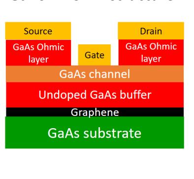
9 Role of graphene Release layer for any semiconductors Dislocation-reducer/filter Release layer 1sec release Wafer Surface protection infinite reuse Wide application of non-si electronics/photonics Enabled heterointegration InP InGaAs GaAs GaN Si wafer

10 Implication for PV technology GaAs substrate
 GaAs(1.42eV) GaInNAs(1eV) Ge(0.67eV) Si (1.")
11 Implication for space PV technology III-V multijunction solar cells for E g oriented design Material 4 Eg~1.8eV Material 3 Eg~1.4eV Material 2 Eg~1eV Material 1 Eg~0.6eV Graphene as dislocation reducer/tunnel junction Examples GaInP(1.87eV) GaAs(1.42eV) GaInNAs(1eV) Ge(0.67eV) Si (1.1 ev) III-V substrate III-V substrate
12 Implication for magnetoelectric coupling Graphene transfer Epitaxy of Piezoelectric materials Exfoliation of Piezoelectric materials Piezo Bonding of freestanding Piezomaterials + magnetostrictive matreials SrTiO 3 SrTiO 3 Graphene transfer SrTiO 3 Remote Exfoliation Epitaxy of Maganetostrictive materials Magneto Piezo PDMS No substrate clamping to Maximize effect MgAl 2 O 4 MgAl 2 O 4 MgAl 2 O 4

 Blue LED (III-N)")


13 Implication for display/lighting technology Low-cost flexible LEDs (solid state lighting/microled) Red LED (III-V) Blue LED (III-N) Dislocation-free LED on graphene Light emission from LEDs on graphene Dislocation-free GaN obtainable by GaN growth on graphene/gan High efficiency lighting High pixel density microled Y. Kim, S. Cruz, J. Kim et al., Nature cover (2017)


14 Implication for power electronics/heterointegration Power electronics
EV Group. Engineered Substrates for future compound semiconductor devices
 EV Group Engineered Substrates for future compound semiconductor devices Engineered Substrates HB-LED: Engineered growth substrates GaN / GaP layer transfer Mobility enhancement solutions: III-Vs to silicon
Currently, worldwide major semiconductor alloy epitaxial growth is divided into two material groups.
 ICQNM 2014 Currently, worldwide major semiconductor alloy epitaxial growth is divided into two material groups. Cubic: Diamond structures: group IV semiconductors (Si, Ge, C), Cubic zinc-blende structures:
ignature redacted Signature redacted -1 Two-Dimensional Material based Layer Transfer of Thin Film Devices JUN LIBRARIES ARCHIVES by Yunjo Kim
 Two-Dimensional Material based Layer Transfer of Thin Film Devices by Yunjo Kim B.A.Sc. Nanotechnology Engineering University of Waterloo, 2015 SUBMITTED TO THE DEPARTMENT OF MECHANICAL ENGINEERING IN
InAs/GaSb Mid-Wave Cascaded Superlattice Light Emitting Diodes
 InAs/GaSb Mid-Wave Cascaded Superlattice Light Emitting Diodes John Prineas Department of Physics and Astronomy, University of Iowa May 3, 206 Collaborator: Thomas Boggess Grad Students: Yigit Aytak Cassandra
III-V nanostructured materials synthesized by MBE droplet epitaxy
 III-V nanostructured materials synthesized by MBE droplet epitaxy E.A. Anyebe 1, C. C. Yu 1, Q. Zhuang 1,*, B. Robinson 1, O Kolosov 1, V. Fal ko 1, R. Young 1, M Hayne 1, A. Sanchez 2, D. Hynes 2, and
2D MBE Activities in Sheffield. I. Farrer, J. Heffernan Electronic and Electrical Engineering The University of Sheffield
 2D MBE Activities in Sheffield I. Farrer, J. Heffernan Electronic and Electrical Engineering The University of Sheffield Outline Motivation Van der Waals crystals The Transition Metal Di-Chalcogenides
High efficiency silicon and perovskite-silicon solar cells for electricity generation
 High efficiency silicon and perovskite-silicon solar cells for electricity generation Ali Dabirian Email: dabirian@ipm.ir 1 From Solar Energy to Electricity 2 Global accumulative PV installed In Iran it
Future Technology Pathways of Terrestrial III-V Multijunction Solar Cells for Concentrator Photovoltaic Systems
 Future Technology Pathways of Terrestrial III-V Multijunction Solar Cells for Concentrator Photovoltaic Systems Daniel C. Law 1,*, R.R. King 1, H. Yoon 1, M.J. Archer 2, A. Boca 1, C.M. Fetzer 1, S. Mesropian
Lecture 30: Kinetics of Epitaxial Growth: Surface Diffusion and
 Lecture 30: Kinetics of Epitaxial Growth: Surface Diffusion and Nucleation Today s topics Understanding the basics of epitaxial techniques used for surface growth of crystalline structures (films, or layers).
An#- Phase- Boundary Defects in GaAs- on- Si Films: 1. characteriza#on by SHG 2. suppression by ART
 Op=cs of Surfaces & Interfaces (OSI - 9) Chemnitz, Germany September 2, 213 An#- Phase- Boundary Defects in GaAs- on- Si Films: 1. characteriza#on by SHG 2. suppression by ART Farbod Shafiei 1, Ming Lei
Graphene films on silicon carbide (SiC) wafers supplied by Nitride Crystals, Inc.
 wafers supplied by Nitride Crystals, Inc.") 9702 Gayton Road, Suite 320, Richmond, VA 23238, USA Phone: +1 (804) 709-6696 info@nitride-crystals.com www.nitride-crystals.com Graphene films on silicon carbide (SiC) wafers supplied by Nitride Crystals,
9702 Gayton Road, Suite 320, Richmond, VA 23238, USA Phone: +1 (804) 709-6696 info@nitride-crystals.com www.nitride-crystals.com Graphene films on silicon carbide (SiC) wafers supplied by Nitride Crystals,
Plan for Lectures #4, 5, & 6. Theme Of Lectures: Nano-Fabrication
 Plan for Lectures #4, 5, & 6 Theme Of Lectures: Nano-Fabrication Quantum Wells, SLs, Epitaxial Quantum Dots Carbon Nanotubes, Semiconductor Nanowires Self-assembly and Self-organization Two Approaches
Physicists in the Semiconductor Industry
 Physicists in the Semiconductor Industry P.M. Mooney IBM Research Division, T.J. Watson Research Center Yorktown Heights, NY 10598 APS March Meeting March 24, 2004 Thomas J. Watson Research Center 1 Outline
Hydrogenated Graphene
 Hydrogenated Graphene Stefan Heun NEST, Istituto Nanoscienze-CNR and Scuola Normale Superiore Pisa, Italy Outline Epitaxial Graphene Hydrogen Chemisorbed on Graphene Hydrogen-Intercalated Graphene Outline
Lecture 1. Introduction to Electronic Materials. Reading: Pierret 1.1, 1.2, 1.4,
 Lecture 1 Introduction to Electronic Materials Reading: Pierret 1.1, 1.2, 1.4, 2.1-2.6 Atoms to Operational Amplifiers The goal of this course is to teach the fundamentals of non-linear circuit elements
Supporting Information. InGaAs Nanomembrane/Si van der Waals Heterojunction. Photodiodes with Broadband and High Photoresponsivity
 Supporting Information InGaAs Nanomembrane/Si van der Waals Heterojunction Photodiodes with Broadband and High Photoresponsivity Doo-Seung Um, Youngsu Lee, Seongdong Lim, Jonghwa Park, Wen-Chun Yen, Yu-Lun
Semiconductor Physics and Devices
 Syllabus Advanced Nano Materials Semiconductor Physics and Devices Textbook Donald A. Neamen (McGraw-Hill) Semiconductor Physics and Devices Seong Jun Kang Department of Advanced Materials Engineering
Band Gap Engineering. Reading the Periodic Table and Understanding Optical and Electrical Properties in Semiconductors
 The Birnie Group solar class and website were created with much-appreciated support from the NSF CRCD Program under grants 0203504 and 0509886. Continuing Support from the McLaren Endowment is also greatly
Optical Investigation of the Localization Effect in the Quantum Well Structures
 Department of Physics Shahrood University of Technology Optical Investigation of the Localization Effect in the Quantum Well Structures Hamid Haratizadeh hamid.haratizadeh@gmail.com IPM, SCHOOL OF PHYSICS,
Temperature Dependent Optical Band Gap Measurements of III-V films by Low Temperature Photoluminescence Spectroscopy
 Temperature Dependent Optical Band Gap Measurements of III-V films by Low Temperature Photoluminescence Spectroscopy Linda M. Casson, Francis Ndi and Eric Teboul HORIBA Scientific, 3880 Park Avenue, Edison,
Protective Catalyst Systems on III-V and Si-based Semiconductors for Efficient, Durable Photoelectrochemical Water Splitting Devices
 Protective Catalyst Systems on III-V and Si-based Semiconductors for Efficient, Durable Photoelectrochemical Water Splitting Devices PI: Thomas Jaramillo 1, co-pi: Jim Harris 2 1 Dept. of Chemical Engineering,
Traps in MOCVD n-gan Studied by Deep Level Transient Spectroscopy and Minority Carrier Transient Spectroscopy
 Traps in MOCVD n-gan Studied by Deep Level Transient Spectroscopy and Minority Carrier Transient Spectroscopy Yutaka Tokuda Department of Electrical and Electronics Engineering, Aichi Institute of Technology,
Self-study problems and questions Processing and Device Technology, FFF110/FYSD13
 Self-study problems and questions Processing and Device Technology, FFF110/FYSD13 Version 2016_01 In addition to the problems discussed at the seminars and at the lectures, you can use this set of problems
Semiconductor Device Physics
 1 Semiconductor Device Physics Lecture 1 http://zitompul.wordpress.com 2 0 1 3 2 Semiconductor Device Physics Textbook: Semiconductor Device Fundamentals, Robert F. Pierret, International Edition, Addison
Wafer-scale fabrication of graphene
 Wafer-scale fabrication of graphene Sten Vollebregt, MSc Delft University of Technology, Delft Institute of Mircosystems and Nanotechnology Delft University of Technology Challenge the future Delft University
Ultrafast single photon emitting quantum photonic structures. based on a nano-obelisk
 Ultrafast single photon emitting quantum photonic structures based on a nano-obelisk Je-Hyung Kim, Young-Ho Ko, Su-Hyun Gong, Suk-Min Ko, Yong-Hoon Cho Department of Physics, Graduate School of Nanoscience
Photodetector. Prof. Woo-Young Choi. Silicon Photonics (2012/2) Photodetection: Absorption => Current Generation. Currents
 Photodetection: Absorption => Current Generation. Currents") Photodetection: Absorption => Current Generation h Currents Materials for photodetection: E g < h Various methods for generating currents with photo-generated carriers: photoconductors, photodiodes, avalanche
Photodetection: Absorption => Current Generation h Currents Materials for photodetection: E g < h Various methods for generating currents with photo-generated carriers: photoconductors, photodiodes, avalanche
Chemistry Instrumental Analysis Lecture 8. Chem 4631
 Chemistry 4631 Instrumental Analysis Lecture 8 UV to IR Components of Optical Basic components of spectroscopic instruments: stable source of radiant energy transparent container to hold sample device
SPCC Department of Bio-Nano Technology and 2 Materials Science and Chemical Engineering, Hanyang University, Ansan, 15588, Republic of Korea.
 SPCC 2018 Hanyang University NEMPL Jin-Goo Park 1,2 *, Jung-Hwan Lee a, In-chan Choi 1, Hyun-Tae Kim 1, Lieve Teugels 3, and Tae-Gon Kim 3 1 Department of Bio-Nano Technology and 2 Materials Science and
The effect of light illumination in photoionization of deep traps in GaN MESFETs buffer layer using an ensemble Monte Carlo simulation
 International Journal of Physical Sciences Vol. 6(2), pp. 273-279, 18 January, 2011 Available online at http://www.academicjournals.org/ijps ISSN 1992-1950 2011 Academic Journals Full Length Research Paper
EE143 Fall 2016 Microfabrication Technologies. Evolution of Devices
 EE143 Fall 2016 Microfabrication Technologies Prof. Ming C. Wu wu@eecs.berkeley.edu 511 Sutardja Dai Hall (SDH) 1-1 Evolution of Devices Yesterday s Transistor (1947) Today s Transistor (2006) 1-2 1 Why
Physics of Semiconductors
 Physics of Semiconductors 9 th 2016.6.13 Shingo Katsumoto Department of Physics and Institute for Solid State Physics University of Tokyo Site for uploading answer sheet Outline today Answer to the question
JOHN G. EKERDT RESEARCH FOCUS
 JOHN G. EKERDT RESEARCH FOCUS We study the surface, growth and materials chemistry of ultrathin metal and dielectric films. Our work seeks to: 1) develop and understand the reactions and chemistry that
Lecture contents. Stress and strain Deformation potential. NNSE 618 Lecture #23
 1 Lecture contents Stress and strain Deformation potential Few concepts from linear elasticity theory : Stress and Strain 6 independent components 2 Stress = force/area ( 3x3 symmetric tensor! ) ij ji
Three-Dimensional Silicon-Germanium Nanostructures for Light Emitters and On-Chip Optical. Interconnects
 Three-Dimensional Silicon-Germanium Nanostructures for Light Emitters and On-Chip Optical eptember 2011 Interconnects Leonid Tsybeskov Department of Electrical and Computer Engineering New Jersey Institute
JOHN G. EKERDT RESEARCH FOCUS
 JOHN G. EKERDT RESEARCH FOCUS We study the surface, growth and materials chemistry of metal, dielectric, ferroelectric, and polymer thin films. We seek to understand and describe nucleation and growth
TFYA23 Crystal Growth Technology
 TFYA23 Crystal Growth Technology Course structure 10 double lectures 2 home assignments 2 laboratories Reporting Written report on the laboratories: SiC growth and characterization, week 49 Problem solutions,
1. Nanotechnology & nanomaterials -- Functional nanomaterials enabled by nanotechnologies.
 Novel Nano-Engineered Semiconductors for Possible Photon Sources and Detectors NAI-CHANG YEH Department of Physics, California Institute of Technology 1. Nanotechnology & nanomaterials -- Functional nanomaterials
Novel materials and nanostructures for advanced optoelectronics
 Novel materials and nanostructures for advanced optoelectronics Q. Zhuang, P. Carrington, M. Hayne, A Krier Physics Department, Lancaster University, UK u Brief introduction to Outline Lancaster University
De De. De M Q fix = const PR R/R Intensity (arb. inits) Energy (ev) a) b)
 Energy (ev) a) b)") PIEZOELECTRIC EFFECTS IN GaInN/GaN HETEROSTRUCTURES AND QUANTUM WELLS C. WETZEL, T. TAKEUCHI, S. YAMAGUCHI, H. KATO, H. AMANO, and I. AKASAKI High Tech Research Center, Meijo University, 1-501 Shiogamaguchi,
PIEZOELECTRIC EFFECTS IN GaInN/GaN HETEROSTRUCTURES AND QUANTUM WELLS C. WETZEL, T. TAKEUCHI, S. YAMAGUCHI, H. KATO, H. AMANO, and I. AKASAKI High Tech Research Center, Meijo University, 1-501 Shiogamaguchi,
Optical properties of indium phosphide inp
 JOURNAL OF OPTOELECTRONICS AND ADVANCED MATERIALS Vol., No. -, May - June, p. 7-7 Optical properties of indium phosphide inp J. O. AKINLAMI *, U. G. IKPEOHA Department of Physics, Federal University of
3-1-2 GaSb Quantum Cascade Laser
 3-1-2 GaSb Quantum Cascade Laser A terahertz quantum cascade laser (THz-QCL) using a resonant longitudinal optical (LO) phonon depopulation scheme was successfully demonstrated from a GaSb/AlSb material
GaN for use in harsh radiation environments
 4 th RD50 - Workshop on radiation hard semiconductor devices for very high luminosity colliders GaN for use in harsh radiation environments a (W Cunningham a, J Grant a, M Rahman a, E Gaubas b, J Vaitkus
Physics and Material Science of Semiconductor Nanostructures
 Physics and Material Science of Semiconductor Nanostructures PHYS 570P Prof. Oana Malis Email: omalis@purdue.edu Course website: http://www.physics.purdue.edu/academic_programs/courses/phys570p/ Lecture
ANTIMONY ENHANCED HOMOGENEOUS NITROGEN INCORPORATION INTO GaInNAs FILMS GROWN BY ATOMIC HYDROGEN-ASSISTED MOLECULAR BEAM EPITAXY
 ANTIMONY ENHANCED HOMOGENEOUS NITROGEN INCORPORATION INTO GaInNAs FILMS GROWN BY ATOMIC HYDROGEN-ASSISTED MOLECULAR BEAM EPITAXY Naoya Miyashita 1, Nazmul Ahsan 1, and Yoshitaka Okada 1,2 1. Research Center
Electrons are shared in covalent bonds between atoms of Si. A bound electron has the lowest energy state.
 Photovoltaics Basic Steps the generation of light-generated carriers; the collection of the light-generated carriers to generate a current; the generation of a large voltage across the solar cell; and
Performance Enhancement of P-channel InGaAs Quantum-well FETs by Superposition of Process-induced Uniaxial Strain and Epitaxially-grown Biaxial Strain
 Performance Enhancement of P-channel InGaAs Quantum-well FETs by Superposition of Process-induced Uniaxial Strain and Epitaxially-grown Biaxial Strain Ling Xia 1, Vadim Tokranov 2, Serge R. Oktyabrsky
EECS143 Microfabrication Technology
 EECS143 Microfabrication Technology Professor Ali Javey Introduction to Materials Lecture 1 Evolution of Devices Yesterday s Transistor (1947) Today s Transistor (2006) Why Semiconductors? Conductors e.g
30 nm In 0.7 Ga 0.3 As Inverted-type HEMT with Reduced Gate Leakage Current for Logic Applications
 30 nm In 0.7 Ga 0.3 As Inverted-type HEMT with Reduced Gate Leakage Current for Logic Applications T.-W. Kim, D.-H. Kim* and J. A. del Alamo Microsystems Technology Laboratories MIT Presently with Teledyne
Optimizing Graphene Morphology on SiC(0001)
") Optimizing Graphene Morphology on SiC(0001) James B. Hannon Rudolf M. Tromp Graphene sheets Graphene sheets can be formed into 0D,1D, 2D, and 3D structures Chemically inert Intrinsically high carrier mobility
Optimizing Graphene Morphology on SiC(0001) James B. Hannon Rudolf M. Tromp Graphene sheets Graphene sheets can be formed into 0D,1D, 2D, and 3D structures Chemically inert Intrinsically high carrier mobility
Vikram L. Dalal Iowa State University Dept. of Elec. And Comp. Engr Iowa State University. All rights reserved.
 Growth Chemistry and Its Relationship to Amorphous Si Devices for Photovoltaic Energy Conversion Vikram L. Dalal Iowa State University Dept. of Elec. And Comp. Engr. 2002 Iowa State University. All rights
Novel High-Efficiency Crystalline-Si-Based Compound. Heterojunction Solar Cells: HCT (Heterojunction with Compound. Thin-layer)
") Electronic Supplementary Material (ESI) for Physical Chemistry Chemical Physics. This journal is the Owner Societies 2014 Supplementary Information for Novel High-Efficiency Crystalline-Si-Based Compound
Electronic Supplementary Material (ESI) for Physical Chemistry Chemical Physics. This journal is the Owner Societies 2014 Supplementary Information for Novel High-Efficiency Crystalline-Si-Based Compound
Quantum and Non-local Transport Models in Crosslight Device Simulators. Copyright 2008 Crosslight Software Inc.
 Quantum and Non-local Transport Models in Crosslight Device Simulators Copyright 2008 Crosslight Software Inc. 1 Introduction Quantization effects Content Self-consistent charge-potential profile. Space
Lectures Graphene and
 Lectures 15-16 Graphene and carbon nanotubes Graphene is atomically thin crystal of carbon which is stronger than steel but flexible, is transparent for light, and conducts electricity (gapless semiconductor).
Band Alignment and Graded Heterostructures. Guofu Niu Auburn University
 Band Alignment and Graded Heterostructures Guofu Niu Auburn University Outline Concept of electron affinity Types of heterojunction band alignment Band alignment in strained SiGe/Si Cusps and Notches at
Intensity (a.u.) Intensity (a.u.) Raman Shift (cm -1 ) Oxygen plasma. 6 cm. 9 cm. 1mm. Single-layer graphene sheet. 10mm. 14 cm
 Intensity (a.u.) Raman Shift (cm -1 ) Oxygen plasma. 6 cm. 9 cm. 1mm. Single-layer graphene sheet. 10mm. 14 cm") Intensity (a.u.) Intensity (a.u.) a Oxygen plasma b 6 cm 1mm 10mm Single-layer graphene sheet 14 cm 9 cm Flipped Si/SiO 2 Patterned chip Plasma-cleaned glass slides c d After 1 sec normal Oxygen plasma
Intensity (a.u.) Intensity (a.u.) a Oxygen plasma b 6 cm 1mm 10mm Single-layer graphene sheet 14 cm 9 cm Flipped Si/SiO 2 Patterned chip Plasma-cleaned glass slides c d After 1 sec normal Oxygen plasma
Electrical isolation of n- and p-in 0.53 Ga 0.47 As epilayers using ion irradiation
 JOURNAL OF APPLIED PHYSICS VOLUME 94, NUMBER 10 15 NOVEMBER 2003 Electrical isolation of n- and p-in 0.53 Ga 0.47 As epilayers using ion irradiation C. Carmody, a) H. H. Tan, and C. Jagadish Department
Organic Electronic Devices
 Organic Electronic Devices Week 5: Organic Light-Emitting Devices and Emerging Technologies Lecture 5.5: Course Review and Summary Bryan W. Boudouris Chemical Engineering Purdue University 1 Understanding
Supplemental Discussion for Multijunction Solar Cell Efficiencies: Effect of Spectral Window, Optical Environment and Radiative Coupling
 Electronic Supplementary Material (ESI) for Energy & Environmental Science. This journal is The Royal Society of Chemistry 2014 Supplemental Discussion for Multijunction Solar Cell Efficiencies: Effect
Self-Assembled InAs Quantum Dots
 Self-Assembled InAs Quantum Dots Steve Lyon Department of Electrical Engineering What are semiconductors What are semiconductor quantum dots How do we make (grow) InAs dots What are some of the properties
Thermoelectric and electrical properties of Si-doped InSb thin films. University, Japan
 10.1149/1.3109626 The Electrochemical Society Thermoelectric and electrical properties of Si-doped InSb thin films H. Nagata a and S. Yamaguchi a,b a Department of Electrical, Electronic and Information
Lecture 12. Semiconductor Detectors - Photodetectors
 Lecture 12 Semiconductor Detectors - Photodetectors Principle of the pn junction photodiode Absorption coefficient and photodiode materials Properties of semiconductor detectors The pin photodiodes Avalanche
Xing Sheng, 微纳光电子材料与器件工艺原理. Doping 掺杂. Xing Sheng 盛兴. Department of Electronic Engineering Tsinghua University
 微纳光电子材料与器件工艺原理 Doping 掺杂 Xing Sheng 盛兴 Department of Electronic Engineering Tsinghua University xingsheng@tsinghua.edu.cn 1 Semiconductor PN Junctions Xing Sheng, EE@Tsinghua LEDs lasers detectors solar
Electron Energy, E E = 0. Free electron. 3s Band 2p Band Overlapping energy bands. 3p 3s 2p 2s. 2s Band. Electrons. 1s ATOM SOLID.
 Electron Energy, E Free electron Vacuum level 3p 3s 2p 2s 2s Band 3s Band 2p Band Overlapping energy bands Electrons E = 0 1s ATOM 1s SOLID In a metal the various energy bands overlap to give a single
OPTI510R: Photonics. Khanh Kieu College of Optical Sciences, University of Arizona Meinel building R.626
 OPTI510R: Photonics Khanh Kieu College of Optical Sciences, University of Arizona kkieu@optics.arizona.edu Meinel building R.626 Announcements HW#3 is assigned due Feb. 20 st Mid-term exam Feb 27, 2PM
3.46 PHOTONIC MATERIALS AND DEVICES Lecture 15: III-V Processing
 3.46 PHOTONIC MATERIALS AND DEVICES 15: III-V Processing Double Hetero structure laser (band structure engineering) AlGaAs GaAs AlGaAs e - E n hν P h + X n x I d < 1 μm 1. Large refractive index active
Epitaxial Growth of InGaAs and InAlAs
 High Growth Temperature Studies of InGaAs/InAlAs Superlattices for High-Quality QCL and QWIP Applications Jiun-Yun Li (a) Fow-Sen Choa, Xiaoming Ji, and Liwei Cheng Department of CSEE University of Maryland
Graphene and Carbon Nanotubes
 Graphene and Carbon Nanotubes 1 atom thick films of graphite atomic chicken wire Novoselov et al - Science 306, 666 (004) 100μm Geim s group at Manchester Novoselov et al - Nature 438, 197 (005) Kim-Stormer
Part 5: Quantum Effects in MOS Devices
 Quantum Effects Lead to Phenomena such as: Ultra Thin Oxides Observe: High Leakage Currents Through the Oxide - Tunneling Depletion in Poly-Si metal gate capacitance effect Thickness of Inversion Layer
Fabrication and Characteristics Study Ni-nSiC Schottky Photodiode Detector
 Fabrication and Characteristics Study Ni-nSiC Schottky Photodiode Detector Muhanad A. Ahamed Department of Electrical, Institution of Technology, Baghdad-Iraq. Abstract In the present work, schottky photodiode
Black phosphorus: A new bandgap tuning knob
 Black phosphorus: A new bandgap tuning knob Rafael Roldán and Andres Castellanos-Gomez Modern electronics rely on devices whose functionality can be adjusted by the end-user with an external knob. A new
EE130: Integrated Circuit Devices
 EE130: Integrated Circuit Devices (online at http://webcast.berkeley.edu) Instructor: Prof. Tsu-Jae King (tking@eecs.berkeley.edu) TA s: Marie Eyoum (meyoum@eecs.berkeley.edu) Alvaro Padilla (apadilla@eecs.berkeley.edu)
New materials for high- efficiency spin-polarized. polarized electron source
 New materials for high- efficiency spin-polarized polarized electron source A. Janotti Metals and Ceramics Division, Oak Ridge National Laboratory, TN In Collaboration with S.-H. Wei, National Renewable
Semi-insulating SiC substrates for high frequency devices
 Klausurtagung Silberbach, 19. - 21. Feb. 2002 Institut für Werkstoffwissenschaften - WW 6 Semi-insulating SiC substrates for high frequency devices Vortrag von Matthias Bickermann Semi-insulating SiC substrates
ET3034TUx Utilization of band gap energy
 ET3034TUx - 3.3.1 - Utilization of band gap energy In the last two weeks we have discussed the working principle of a solar cell and the external parameters that define the performance of a solar cell.
Halbleiter. Prof. Yong Lei. Prof. Thomas Hannappel.
 Halbleiter Prof. Yong Lei Prof. Thomas Hannappel yong.lei@tu-ilemnau.de thomas.hannappel@tu-ilmenau.de Important Events in Semiconductors History 1833 Michael Faraday discovered temperature-dependent conductivity
Feature-level Compensation & Control. Process Integration September 15, A UC Discovery Project
 Feature-level Compensation & Control Process Integration September 15, 2005 A UC Discovery Project Current Milestones Si/Ge-on-insulator and Strained Si-on-insulator Substrate Engineering (M28 YII.13)
Ferromagnetism and Anomalous Hall Effect in Graphene
 Ferromagnetism and Anomalous Hall Effect in Graphene Jing Shi Department of Physics & Astronomy, University of California, Riverside Graphene/YIG Introduction Outline Proximity induced ferromagnetism Quantized
Molecular Solar Cells Progress Report
 MolecularSolarCellsProgressReport Investigators Faculty:Prof.PeterPeumans(ElectricalEngineering,Stanford) Graduateresearchers:MukulAgrawal,ShanbinZhao,AlbertLiu,SeungRim,Jung YongLee,JunboWu Summary We
(Co-PIs-Mark Brongersma, Yi Cui, Shanhui Fan) Stanford University. GCEP Research Symposium 2013 Stanford, CA October 9, 2013
 Stanford University. GCEP Research Symposium 2013 Stanford, CA October 9, 2013") High-efficiency thin film nano-structured multi-junction solar James S. cells Harris (PI) (Co-PIs-Mark Brongersma, Yi Cui, Shanhui Fan) Stanford University GCEP Research Symposium 2013 Stanford, CA October
High-efficiency thin film nano-structured multi-junction solar James S. cells Harris (PI) (Co-PIs-Mark Brongersma, Yi Cui, Shanhui Fan) Stanford University GCEP Research Symposium 2013 Stanford, CA October
Theory of Hydrogen-Related Levels in Semiconductors and Oxides
 Theory of Hydrogen-Related Levels in Semiconductors and Oxides Chris G. Van de Walle Materials Department University of California, Santa Barbara Acknowledgments Computations J. Neugebauer (Max-Planck-Institut,
Introduction to semiconductor nanostructures. Peter Kratzer Modern Concepts in Theoretical Physics: Part II Lecture Notes
 Introduction to semiconductor nanostructures Peter Kratzer Modern Concepts in Theoretical Physics: Part II Lecture Notes What is a semiconductor? The Fermi level (chemical potential of the electrons) falls
Structural and Optical Properties of ZnSe under Pressure
 www.stmjournals.com Structural and Optical Properties of ZnSe under Pressure A. Asad, A. Afaq* Center of Excellence in Solid State Physics, University of the Punjab Lahore-54590, Pakistan Abstract The
A semiconductor is an almost insulating material, in which by contamination (doping) positive or negative charge carriers can be introduced.
 positive or negative charge carriers can be introduced.") Semiconductor A semiconductor is an almost insulating material, in which by contamination (doping) positive or negative charge carriers can be introduced. Page 2 Semiconductor materials Page 3 Energy levels
Semiconductor A semiconductor is an almost insulating material, in which by contamination (doping) positive or negative charge carriers can be introduced. Page 2 Semiconductor materials Page 3 Energy levels
Surface physics, Bravais lattice
 Surface physics, Bravais lattice 1. Structure of the solid surface characterized by the (Bravais) lattice + space + point group lattice describes also the symmetry of the solid material vector directions
Figure 1: Graphene release, transfer and stacking processes. The graphene stacking began with CVD
 Supplementary figure 1 Graphene Growth and Transfer Graphene PMMA FeCl 3 DI water Copper foil CVD growth Back side etch PMMA coating Copper etch in 0.25M FeCl 3 DI water rinse 1 st transfer DI water 1:10
A. Optimizing the growth conditions of large-scale graphene films
 1 A. Optimizing the growth conditions of large-scale graphene films Figure S1. Optical microscope images of graphene films transferred on 300 nm SiO 2 /Si substrates. a, Images of the graphene films grown
Initial Stages of Growth of Organic Semiconductors on Graphene
 Initial Stages of Growth of Organic Semiconductors on Graphene Presented by: Manisha Chhikara Supervisor: Prof. Dr. Gvido Bratina University of Nova Gorica Outline Introduction to Graphene Fabrication
Widely Tunable and Intense Mid-Infrared PL Emission from Epitaxial Pb(Sr)Te Quantum Dots in a CdTe Matrix
Te Quantum Dots in a CdTe Matrix") Widely Tunable and Intense Mid-Infrared PL Emission from Epitaxial Pb(Sr)Te Quantum Dots in a Matrix S. Kriechbaumer 1, T. Schwarzl 1, H. Groiss 1, W. Heiss 1, F. Schäffler 1,T. Wojtowicz 2, K. Koike 3,
Widely Tunable and Intense Mid-Infrared PL Emission from Epitaxial Pb(Sr)Te Quantum Dots in a Matrix S. Kriechbaumer 1, T. Schwarzl 1, H. Groiss 1, W. Heiss 1, F. Schäffler 1,T. Wojtowicz 2, K. Koike 3,
Naser M. Ahmed *, Zaliman Sauli, Uda Hashim, Yarub Al-Douri. Abstract
 Int. J. Nanoelectronics and Materials (009) 89-95 Investigation of the absorption coefficient, refractive index, energy band gap, and film thickness for Al 0. Ga 0.89 N, Al 0.03 Ga 0.97 N, and GaN by optical
Spontaneous lateral composition modulation in InAlAs and InGaAs short-period superlattices
 Physica E 2 (1998) 325 329 Spontaneous lateral composition modulation in InAlAs and InGaAs short-period superlattices D.M. Follstaedt *, R.D. Twesten, J. Mirecki Millunchick, S.R. Lee, E.D. Jones, S.P.
Thermal Stress and Strain in a GaN Epitaxial Layer Grown on a Sapphire Substrate by the MOCVD Method
 CHINESE JOURNAL OF PHYSICS VOL. 48, NO. 3 June 2010 Thermal Stress and Strain in a GaN Epitaxial Layer Grown on a Sapphire Substrate by the MOCVD Method H. R. Alaei, 1 H. Eshghi, 2 R. Riedel, 3 and D.
Optical properties of strain-compensated hybrid InGaN/InGaN/ZnO quantum well lightemitting
 Optical properties of strain-compensated hybrid InGaN/InGaN/ZnO quantum well lightemitting diodes S.-H. Park 1, S.-W. Ryu 1, J.-J. Kim 1, W.-P. Hong 1, H.-M Kim 1, J. Park 2, and Y.-T. Lee 3 1 Department
Optical Absorption Enhancement in Freestanding GaAs Thin Film Nanopyramid Arrays
 Optical Absorption Enhancement in Freestanding GaAs Thin Film Nanopyramid Arrays Dong Liang, * Yijie Huo, Yangsen Kang, Ken Xingze Wang, Anjia Gu, Meiyueh Tan, Zongfu Yu, Shuang Li, Jieyang Jia, Xinyu
PHOTOLUMINESCENCE STUDY OF INGAAS/GAAS QUANTUM DOTS
 PHOTOLUMINESCENCE STUDY OF INGAAS/GAAS QUANTUM DOTS A. Majid a,b, Samir Alzobaidi a and Thamer Alharbi a a Department of Physics, College of Science, Almajmaah University, P. O. Box no.1712, Al-Zulfi 11932,
Growth optimization of InGaAs quantum wires for infrared photodetector applications
 Growth optimization of InGaAs quantum wires for infrared photodetector applications Chiun-Lung Tsai, Chaofeng Xu, K. C. Hsieh, and K. Y. Cheng a Department of Electrical and Computer Engineering and Micro
GaN based transistors
 GaN based transistors S FP FP dielectric G SiO 2 Al x Ga 1-x N barrier i-gan Buffer i-sic D Transistors "The Transistor was probably the most important invention of the 20th Century The American Institute
Multijunction Solar Cells on Epitaxial Templates
 Multijunction Solar Cells on Epitaxial Templates Thesis by Melissa Jane Archer In Partial Fulfillment of the Requirements for the Degree of Doctor of Philosophy California Institute of Technology Pasadena,
XPS Depth Profiling of Epitaxial Graphene Intercalated with FeCl 3
 XPS Depth Profiling of Epitaxial Graphene Intercalated with FeCl 3 Mahdi Ibrahim Maynard H. Jackson High School Atlanta, GA. Faculty Advisor: Dr. Kristin Shepperd Research Group: Prof. Edward Conrad School
Electronic Materials, Heterostrucuture Semiconductor, Light Emitting Devices, Molecular Beam Epitaxy
 REPORT DOCUMENTATION PAGE Form Approved OMB No. 0704-0188 The public reporting burden for this collection of information is estimated to average 1 hour per response, including the time for reviewing instructions,