Xing Sheng, 微纳光电子材料与器件工艺原理. Doping 掺杂. Xing Sheng 盛兴. Department of Electronic Engineering Tsinghua University
|
|
|
- Juniper Randall
- 5 years ago
- Views:
Transcription


1 微纳光电子材料与器件工艺原理 Doping 掺杂 Xing Sheng 盛兴 Department of Electronic Engineering Tsinghua University 1
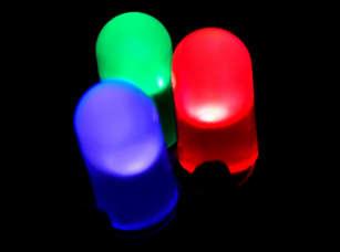
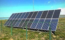
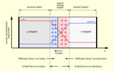
2 Semiconductor PN Junctions Xing Sheng, LEDs lasers detectors solar cells 5
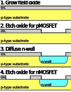
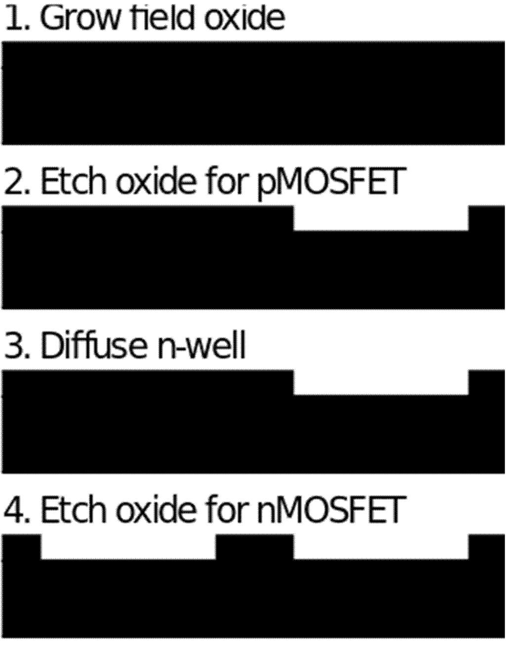
3 CMOS Transistors 6
4 CMOS Transistors 7

5 Doping ingots and wafers 8

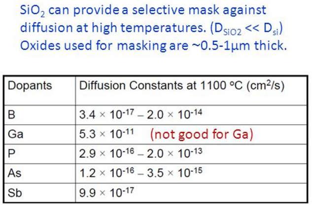
6 For silicon: p dopant: B, Al, Ga,... n dopant: P, As, Sb,... germanium is similar to Si. Doping in Silicon 9

7 For silicon: p dopant: B, Al, Ga,... n dopant: P, As, Sb,... Doping in Silicon 10

8 Doping in GaAs For GaAs: p dopant: replace Ga: Mg, Zn, Be replace As: C... n dopant: replace As: Se replace Ga: Si, Ge... 11
9 Doping Methods Thermal diffusion Ion implantation In situ growth 12
10 Thermal Diffusion - Silicon Xing Sheng, EE@Tsinghua Sources Phosphorus (P) Liquid - POCl 3 Gas - PH 3 Boron (B) Liquid - BBr 3 Solid - B 2 O 3 Gas - B 2 H 6 Arsenic (As) Solid - As 2 O 3 Gas - AsH 3 13
11 Thermal Diffusion - Silicon Xing Sheng, EE@Tsinghua Gas Source Diffusion 14
12 Thermal Diffusion - Silicon Xing Sheng, EE@Tsinghua Liquid Source Diffusion 15
13 Thermal Diffusion - Silicon Xing Sheng, EE@Tsinghua Solid Source Diffusion 16

14 Thermal Diffusion - Silicon Xing Sheng, EE@Tsinghua Spin-on doping 17

15 Thermal Diffusion Process Parameters Time Temperature Gas pressure Gas flow rate Control Parameters Junction depth Doping concentration Doping profile 18
 diffusivity (m 2 /s)")
16 Diffusion Law Liquid Solid C concentration (mol/m 3 ) J D diffusion flux (mol/m 2 /s) diffusivity (m 2 /s) 19
17 Diffusion Law Fick's first law 1D J D C x 3D J DC Fick's second law C t D 2 C 2 x t C 2 1D 3D D C J: mol/m 2 /s D: m 2 /s C: mol/m 3 20
 Diffusion length L slow L Dt diffusivity of defects in Si")
18 Dopant Diffusivity in Silicon Diffusivity ( 扩散系数 ) D rate of spread unit: cm 2 /s fast D D 0 exp( E A kt ) Diffusion length L slow L Dt diffusivity of defects in Si 21

19 Dopant Diffusivity in Silicon Xing Sheng, B, P, As, Sb, Si,... Cu, Fe, Li, H, Au,... 22
20 Dopant Solubility in Silicon maximum dopant amount in silicon Xing Sheng, 23
21 Dopant Diffusion in Silicon when the source is semi-infinite, and the surface is at the solubility limit C ss Xing Sheng, EE@Tsinghua C D t C( x 0, t C( x, t C( x 0, t 2 C 2 x 0) 0) 0) 0 0 C ss C( x, t) source Si C ss erfc x 2 Dt Error Function x 24
22 Dopant Diffusion in Silicon when the source is semi-infinite, and the surface is at the solubility limit C ss Xing Sheng, EE@Tsinghua source Si x C( x, t) C ss erfc 2 x Dt 25
23 Dopant Diffusion in Silicon when the source is limited, Xing Sheng, C( x C( x C D t 0, t 0, t C( x, t 2 C 2 x 0) 0) 0) Q 0 0 C( x, t) Si Q Dt exp Gaussian Function 2 x 4Dt x 26
24 Dopant Diffusion in Silicon when the source is limited, Xing Sheng, Si x C( x, t) Q Dt exp 2 x 4Dt Gaussian Function 27

25 Diffusion Masks Q: why not photoresist? 28

26 Laser Assisted Annealing Xing Sheng, local heating 29
27 Doping Methods Thermal diffusion Ion implantation In situ growth 30


28 Ion Implantation ( 离子注入 ) Xing Sheng, EE@Tsinghua 31
29 Ion Implantation - Advantages Xing Sheng, EE@Tsinghua Precise control of dose, depth and profile Low temperature process Tailor lateral distribution Wide selection of dopants 32
30 Ion Implantation - Advantages Xing Sheng, EE@Tsinghua Precise control of dose, depth and profile vs. Thermal diffusion Ion implantation 33

31 Ion Implantation - Advantages Low temperature process implantation at room temperature mask materials: photoresist, SiO 2, metal,... Lateral distribution Thermal diffusion Ion implantation 34

32 Ion Implantation - Advantages Low temperature process implantation at room temperature mask materials: photoresist, SiO 2, metal,... Lateral distribution shadow effect 35

33 Self Alignment n dopant n-si n-si p-si n-si 36
34 Dopant Distribution Process Parameters dopant type (B, P, As, Sb,...) implantation dose (# /cm 2 ) energy (ev) substrate orientation anneal time, temperature Control Parameters Junction depth Doping concentration Doping profile 37


35 Simulation Software - SRIM Xing Sheng, EE@Tsinghua 38
36 Dopant Distribution dopant type 39

37 Dopant Distribution dose 40
38 Dopant Distribution energy 41
39 Dopant Distribution Ideal case: Gaussian profile 42
40 Dopant Distribution Light atoms (e.g. B): back scattering Heavy atoms (e.g. Sb): forward scattering 43

41 Dopant Distribution ( 沟道效应 ) 44
42 Dopant Distribution ion channeling 45


43 Reduce Channeling Effects Xing Sheng, tilt the crystal form a thin oxide layer damage the surface by implantation 46
44 Video: Bullet in gel Implantation Damage Xing Sheng, amorphous 47


45 Implantation Damage Xing Sheng, anneal & activation 48
46 Effect of Annealing x C D t C 0 0), ( ) ( 0), ( 0 t x C x C t x C Dt x x C t x C 4 exp ) ( ), ( 2 0

47 Make Silicon-on-Insulator (SOI) oxygen ion implant 'SIMOX' Separation by IMplanted OXygen 50

48 Make Silicon-on-Insulator (SOI) 'Smart-Cut' 51
49 Doping Methods Thermal diffusion Ion implantation In situ growth 52
 3 + AsH 3 GaAs + 3CH 4 add")

50 Doping of Gallium Arsenide (GaAs) GaAs growth MOCVD: Ga(CH 3 ) 3 + AsH 3 GaAs + 3CH 4 add dopant gas: SiH 4, Mg, Zn,... vertical structures with high quality thin-films Example: GaAs solar cell 53

51 GaAs VCSEL Vertical Cavity Surface Emitting Laser growth with in situ doping isolation by ion implantation ion implanted (H +, O -,...) region for isolation highly damaged and resistive region 54


52 Doping of Gallium Nitride (GaN) n-gan is easy use Si to replace Ga p-gan is very difficult use Mg to replace Ga, but... Mg deep level acceptor H. Amano, et al., Jpn. J. Appl. Phys. 28, L2112 (1989) S. Nakamura, et al., Appl. Phys. Lett. 64, 1687 (1994) I. Akasaki H. Amano S. Nakamura 2014 Nobel Prize in Physics hydrogen reduces distortion 55

53 Doping Measurement Xing Sheng, 56
 e C( x) 1 ( x) sheet resistance 1 R s x t 0 ( x) dx")
54 Resistivity Four Point Probe Measurement conductivity ( x) e C( x) 1 ( x) sheet resistance 1 R s x t 0 ( x) dx 57

55 SIMS SIMS: Secondary Ion Mass Spectroscopy equipment similar with ion implantation 58
56 Thank you for your attention 60
Ion Implantation ECE723
 Ion Implantation Topic covered: Process and Advantages of Ion Implantation Ion Distribution and Removal of Lattice Damage Simulation of Ion Implantation Range of Implanted Ions Ion Implantation is the
Ion Implant Part 1. Saroj Kumar Patra, TFE4180 Semiconductor Manufacturing Technology. Norwegian University of Science and Technology ( NTNU )
") 1 Ion Implant Part 1 Chapter 17: Semiconductor Manufacturing Technology by M. Quirk & J. Serda Spring Semester 2014 Saroj Kumar Patra,, Norwegian University of Science and Technology ( NTNU ) 2 Objectives
1 Ion Implant Part 1 Chapter 17: Semiconductor Manufacturing Technology by M. Quirk & J. Serda Spring Semester 2014 Saroj Kumar Patra,, Norwegian University of Science and Technology ( NTNU ) 2 Objectives
A semiconductor is an almost insulating material, in which by contamination (doping) positive or negative charge carriers can be introduced.
 positive or negative charge carriers can be introduced.") Semiconductor A semiconductor is an almost insulating material, in which by contamination (doping) positive or negative charge carriers can be introduced. Page 2 Semiconductor materials Page 3 Energy levels
Semiconductor A semiconductor is an almost insulating material, in which by contamination (doping) positive or negative charge carriers can be introduced. Page 2 Semiconductor materials Page 3 Energy levels
Section 7: Diffusion. Jaeger Chapter 4. EE143 Ali Javey
 Section 7: Diffusion Jaeger Chapter 4 Surface Diffusion: Dopant Sources (a) Gas Source: AsH 3, PH 3, B 2 H 6 (b) Solid Source BN Si BN Si (c) Spin-on-glass SiO 2 +dopant oxide (d) Liquid Source. Fick s
Photolithography 光刻 Part II: Photoresists
 微纳光电子材料与器件工艺原理 Photolithography 光刻 Part II: Photoresists Xing Sheng 盛兴 Department of Electronic Engineering Tsinghua University xingsheng@tsinghua.edu.cn 1 Photolithography 光刻胶 负胶 正胶 4 Photolithography
Dopant Diffusion. (1) Predeposition dopant gas. (2) Drive-in Turn off dopant gas. dose control. Doped Si region
 Predeposition dopant gas. (2) Drive-in Turn off dopant gas. dose control. Doped Si region") Dopant Diffusion (1) Predeposition dopant gas dose control SiO Si SiO Doped Si region () Drive-in Turn off dopant gas or seal surface with oxide profile control (junction depth; concentration) SiO SiO
Dopant Diffusion (1) Predeposition dopant gas dose control SiO Si SiO Doped Si region () Drive-in Turn off dopant gas or seal surface with oxide profile control (junction depth; concentration) SiO SiO
Review of Semiconductor Fundamentals
 ECE 541/ME 541 Microelectronic Fabrication Techniques Review of Semiconductor Fundamentals Zheng Yang (ERF 3017, email: yangzhen@uic.edu) Page 1 Semiconductor A semiconductor is an almost insulating material,
Diffusion and Ion implantation Reference: Chapter 4 Jaeger or Chapter 3 Ruska N & P Dopants determine the resistivity of material Note N lower
 Diffusion and Ion implantation Reference: Chapter 4 Jaeger or Chapter 3 Ruska N & P Dopants determine the resistivity of material Note N lower resistavity than p: due to higher carrier mobility Near linear
Semiconductors Reference: Chapter 4 Jaeger or Chapter 3 Ruska Recall what determines conductor, insulator and semiconductor Plot the electron energy
 Semiconductors Reference: Chapter 4 Jaeger or Chapter 3 Ruska Recall what determines conductor, insulator and semiconductor Plot the electron energy states of a material In some materials get the creation
Dopant Diffusion Sources
 Dopant Diffusion (1) Predeposition dopant gas dose control SiO Si SiO Doped Si region () Drive-in Turn off dopant gas or seal surface with oide profile control (junction depth; concentration) SiO SiO Si
Ion Implantation. alternative to diffusion for the introduction of dopants essentially a physical process, rather than chemical advantages:
 Ion Implantation alternative to diffusion for the introduction of dopants essentially a physical process, rather than chemical advantages: mass separation allows wide varies of dopants dose control: diffusion
Properties of Error Function erf(z) And Complementary Error Function erfc(z)
 And Complementary Error Function erfc(z)") Properties of Error Function erf(z) And Complementary Error Function erfc(z) z erf (z) π e -y dy erfc (z) 1 - erf (z) erf () erf( ) 1 erf(- ) - 1 erf (z) d erf(z) dz π z for z
Properties of Error Function erf(z) And Complementary Error Function erfc(z) z erf (z) π e -y dy erfc (z) 1 - erf (z) erf () erf( ) 1 erf(- ) - 1 erf (z) d erf(z) dz π z for z
DIFFUSION - Chapter 7
 DIFFUSION - Chapter 7 Doping profiles determine many short-channel characteristics in MOS devices. Resistance impacts drive current. Scaling implies all lateral and vertical dimensions scale by the same
Introduction to Semiconductor Physics. Prof.P. Ravindran, Department of Physics, Central University of Tamil Nadu, India
 Introduction to Semiconductor Physics 1 Prof.P. Ravindran, Department of Physics, Central University of Tamil Nadu, India http://folk.uio.no/ravi/cmp2013 Review of Semiconductor Physics Semiconductor fundamentals
Ga and P Atoms to Covalent Solid GaP
 Ga and P Atoms to Covalent Solid GaP Band Gaps in Binary Group III-V Semiconductors Mixed Semiconductors Affect of replacing some of the As with P in GaAs Band Gap (ev) (nm) GaAs 1.35 919 (IR) GaP 2.24
Fabrication Technology, Part I
 EEL5225: Principles of MEMS Transducers (Fall 2004) Fabrication Technology, Part I Agenda: Microfabrication Overview Basic semiconductor devices Materials Key processes Oxidation Thin-film Deposition Reading:
September 21, 2005, Wednesday
 , Wednesday Doping and diffusion I Faster MOSFET requires shorter channel P + Poly Al Al Motivation Requires shallower source, drain Al P + Poly Al source drain Shorter channel length; yes, but same source
UNIVERSITY OF CALIFORNIA College of Engineering Department of Electrical Engineering and Computer Sciences. Fall Exam 1
 UNIVERSITY OF CALIFORNIA College of Engineering Department of Electrical Engineering and Computer Sciences EECS 143 Fall 2008 Exam 1 Professor Ali Javey Answer Key Name: SID: 1337 Closed book. One sheet
Chapter 1 Overview of Semiconductor Materials and Physics
 Chapter 1 Overview of Semiconductor Materials and Physics Professor Paul K. Chu Conductivity / Resistivity of Insulators, Semiconductors, and Conductors Semiconductor Elements Period II III IV V VI 2 B
Chapter 8 Ion Implantation
 Chapter 8 Ion Implantation 2006/5/23 1 Wafer Process Flow Materials IC Fab Metalization CMP Dielectric deposition Test Wafers Masks Thermal Processes Implant PR strip Etch PR strip Packaging Photolithography
Dopant and Self-Diffusion in Semiconductors: A Tutorial
 Dopant and Self-Diffusion in Semiconductors: A Tutorial Eugene Haller and Hughes Silvestri MS&E, UCB and LBNL FLCC Tutorial 1/26/04 1 FLCC Outline Motivation Background Fick s Laws Diffusion Mechanisms
Lecture 5. Ion Implantation. Reading: Chapter 5
 Lecture 5 Ion Implantation Reading: Chapter 5 Shockley patented the concept of Ion Implantation for semiconductor doping in 956 ( years after Pfann patented the diffusion concept). First commercial implanters
Make sure the exam paper has 9 pages (including cover page) + 3 pages of data for reference
 + 3 pages of data for reference") UNIVERSITY OF CALIFORNIA College of Engineering Department of Electrical Engineering and Computer Sciences Spring 2006 EE143 Midterm Exam #1 Family Name First name SID Signature Make sure the exam paper
UNIVERSITY OF CALIFORNIA College of Engineering Department of Electrical Engineering and Computer Sciences Spring 2006 EE143 Midterm Exam #1 Family Name First name SID Signature Make sure the exam paper
Self-study problems and questions Processing and Device Technology, FFF110/FYSD13
 Self-study problems and questions Processing and Device Technology, FFF110/FYSD13 Version 2016_01 In addition to the problems discussed at the seminars and at the lectures, you can use this set of problems
Electronics The basics of semiconductor physics
 Electronics The basics of semiconductor physics Prof. Márta Rencz, Gergely Nagy BME DED September 16, 2013 The basic properties of semiconductors Semiconductors conductance is between that of conductors
High-Precision Evaluation of Ultra-Shallow Impurity Profiles by Secondary Ion Mass Spectrometry
 High-Precision Evaluation of Ultra-Shallow Impurity Profiles by Secondary Ion Mass Spectrometry Yoko Tada Kunihiro Suzuki Yuji Kataoka (Manuscript received December 28, 2009) As complementary metal oxide
Classification of Solids
 Classification of Solids Classification by conductivity, which is related to the band structure: (Filled bands are shown dark; D(E) = Density of states) Class Electron Density Density of States D(E) Examples
UNIVERSITY OF CALIFORNIA. College of Engineering. Department of Electrical Engineering and Computer Sciences. Professor Ali Javey.
 UNIVERSITY OF CALIFORNIA College of Engineering Department of Electrical Engineering and Computer Sciences EE 143 Professor Ali Javey Spring 2009 Exam 2 Name: SID: Closed book. One sheet of notes is allowed.
Single ion implantation for nanoelectronics and the application to biological systems. Iwao Ohdomari Waseda University Tokyo, Japan
 Single ion implantation for nanoelectronics and the application to biological systems Iwao Ohdomari Waseda University Tokyo, Japan Contents 1.History of single ion implantation (SII) 2.Novel applications
Quiz #1 Practice Problem Set
 Name: Student Number: ELEC 3908 Physical Electronics Quiz #1 Practice Problem Set? Minutes January 22, 2016 - No aids except a non-programmable calculator - All questions must be answered - All questions
EE 212 FALL ION IMPLANTATION - Chapter 8 Basic Concepts
 EE 212 FALL 1999-00 ION IMPLANTATION - Chapter 8 Basic Concepts Ion implantation is the dominant method of doping used today. In spite of creating enormous lattice damage it is favored because: Large range
EECS130 Integrated Circuit Devices
 EECS130 Integrated Circuit Devices Professor Ali Javey 8/30/2007 Semiconductor Fundamentals Lecture 2 Read: Chapters 1 and 2 Last Lecture: Energy Band Diagram Conduction band E c E g Band gap E v Valence
Chapter 3 Engineering Science for Microsystems Design and Fabrication
 Lectures on MEMS and MICROSYSTEMS DESIGN and MANUFACTURE Chapter 3 Engineering Science for Microsystems Design and Fabrication In this Chapter, we will present overviews of the principles of physical and
MATHEMATICS OF DOPING PROFILES. C(x,t) t. = D 2 C(x,t) x 2. 4Dt dx '
 t. = D 2 C(x,t) x 2. 4Dt dx '") EE43 MATHEMATICS OF DOPING PROFILES N. Cheung The diffusion equation with constant D : has the general solution: C(x,t) = C(x,t) = D 2 C(x,t) 4πDt F(x ' ) e -(x-x' ) 2 4Dt dx ' - where F(x') is the C(x,t)
EE43 MATHEMATICS OF DOPING PROFILES N. Cheung The diffusion equation with constant D : has the general solution: C(x,t) = C(x,t) = D 2 C(x,t) 4πDt F(x ' ) e -(x-x' ) 2 4Dt dx ' - where F(x') is the C(x,t)
Semi-insulating SiC substrates for high frequency devices
 Klausurtagung Silberbach, 19. - 21. Feb. 2002 Institut für Werkstoffwissenschaften - WW 6 Semi-insulating SiC substrates for high frequency devices Vortrag von Matthias Bickermann Semi-insulating SiC substrates
Lecture 150 Basic IC Processes (10/10/01) Page ECE Analog Integrated Circuits and Systems P.E. Allen
 Page ECE Analog Integrated Circuits and Systems P.E. Allen") Lecture 150 Basic IC Processes (10/10/01) Page 1501 LECTURE 150 BASIC IC PROCESSES (READING: TextSec. 2.2) INTRODUCTION Objective The objective of this presentation is: 1.) Introduce the fabrication of
Lecture 150 Basic IC Processes (10/10/01) Page 1501 LECTURE 150 BASIC IC PROCESSES (READING: TextSec. 2.2) INTRODUCTION Objective The objective of this presentation is: 1.) Introduce the fabrication of
Modelling for Formation of Source/Drain Region by Ion Implantation and Diffusion Process for MOSFET Device
 Modelling for Formation of Source/Drain Region by Ion Implantation and Diffusion Process for MOSFET Device 1 Supratim Subhra Das 2 Ria Das 1,2 Assistant Professor, Mallabhum Institute of Technology, Bankura,
ION IMPLANTATION - Chapter 8 Basic Concepts
 ION IMPLANTATION - Chapter 8 Basic Concepts Ion implantation is the dominant method of doping used today. In spite of creating enormous lattice damage it is favored because: Large range of doses - 1 11
Traps in MOCVD n-gan Studied by Deep Level Transient Spectroscopy and Minority Carrier Transient Spectroscopy
 Traps in MOCVD n-gan Studied by Deep Level Transient Spectroscopy and Minority Carrier Transient Spectroscopy Yutaka Tokuda Department of Electrical and Electronics Engineering, Aichi Institute of Technology,
EECS143 Microfabrication Technology
 EECS143 Microfabrication Technology Professor Ali Javey Introduction to Materials Lecture 1 Evolution of Devices Yesterday s Transistor (1947) Today s Transistor (2006) Why Semiconductors? Conductors e.g
CLASS 12th. Semiconductors
 CLASS 12th Semiconductors 01. Distinction Between Metals, Insulators and Semi-Conductors Metals are good conductors of electricity, insulators do not conduct electricity, while the semiconductors have
Feature-level Compensation & Control. Process Integration September 15, A UC Discovery Project
 Feature-level Compensation & Control Process Integration September 15, 2005 A UC Discovery Project Current Milestones Si/Ge-on-insulator and Strained Si-on-insulator Substrate Engineering (M28 YII.13)
Lecture 1. OUTLINE Basic Semiconductor Physics. Reading: Chapter 2.1. Semiconductors Intrinsic (undoped) silicon Doping Carrier concentrations
 silicon Doping Carrier concentrations") Lecture 1 OUTLINE Basic Semiconductor Physics Semiconductors Intrinsic (undoped) silicon Doping Carrier concentrations Reading: Chapter 2.1 EE105 Fall 2007 Lecture 1, Slide 1 What is a Semiconductor? Low
Lecture 1 OUTLINE Basic Semiconductor Physics Semiconductors Intrinsic (undoped) silicon Doping Carrier concentrations Reading: Chapter 2.1 EE105 Fall 2007 Lecture 1, Slide 1 What is a Semiconductor? Low
Chapter 9 Ion Implantation
 Chapter 9 Ion Implantation Professor Paul K. Chu Ion Implantation Ion implantation is a low-temperature technique for the introduction of impurities (dopants) into semiconductors and offers more flexibility
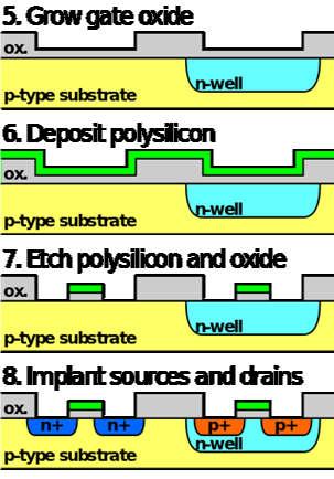
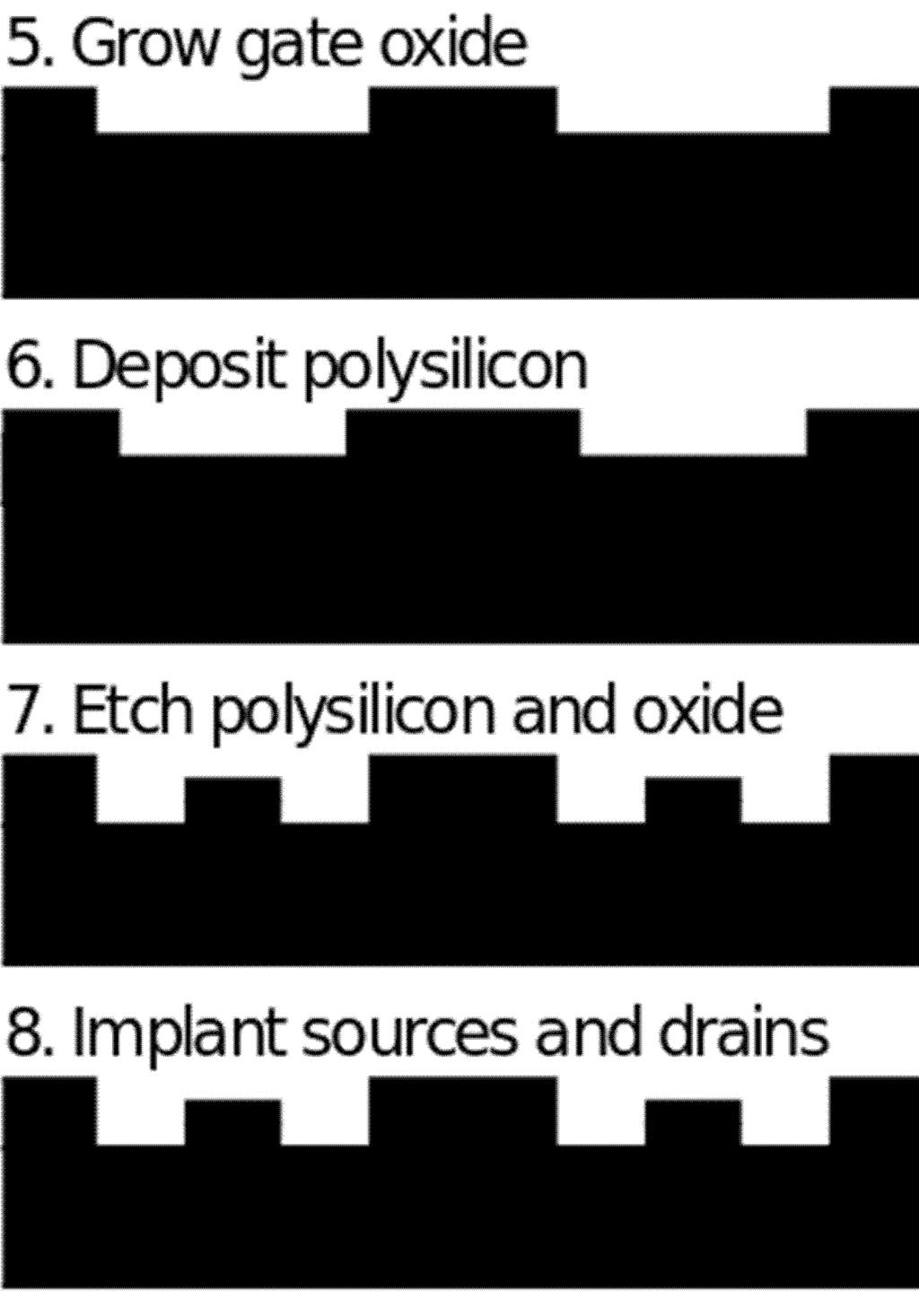
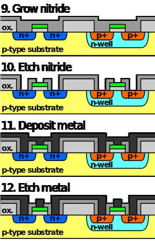
Changing the Dopant Concentration. Diffusion Doping Ion Implantation
 Changing the Dopant Concentration Diffusion Doping Ion Implantation Step 11 The photoresist is removed with solvent leaving a ridge of polysilicon (the transistor's gate), which rises above the silicon
Semiconductor Physics and Devices
 Syllabus Advanced Nano Materials Semiconductor Physics and Devices Textbook Donald A. Neamen (McGraw-Hill) Semiconductor Physics and Devices Seong Jun Kang Department of Advanced Materials Engineering
EE143 Fall 2016 Microfabrication Technologies. Evolution of Devices
 EE143 Fall 2016 Microfabrication Technologies Prof. Ming C. Wu wu@eecs.berkeley.edu 511 Sutardja Dai Hall (SDH) 1-1 Evolution of Devices Yesterday s Transistor (1947) Today s Transistor (2006) 1-2 1 Why
Chapter 3 Basics Semiconductor Devices and Processing
 Chapter 3 Basics Semiconductor Devices and Processing Hong Xiao, Ph. D. www2.austin.cc.tx.us/hongxiao/book.htm Hong Xiao, Ph. D. www2.austin.cc.tx.us/hongxiao/book.htm 1 Objectives Identify at least two
Introduction to Photolithography
 http://www.ichaus.de/news/72 Introduction to Photolithography Photolithography The following slides present an outline of the process by which integrated circuits are made, of which photolithography is
Dependence of Hole Concentration in p-type Silicon Solar Cell Wafers on Temperature and on Position within the Polycrystalline Ingot
 Dependence of Hole Concentration in p-type Silicon Solar Cell Wafers on Temperature and on Position within the Polycrystalline Ingot H. Matsuura, T. Ishida, K. ishikawa. Fukunaga and T. Kuroda Department
Thermal Oxidation of Si
 Thermal Oxidation of General Properties of O 2 Applications of thermal O 2 Deal-Grove Model of Oxidation Thermal O 2 is amorphous. Weight Density = 2.20 gm/cm 3 Molecular Density = 2.3E22 molecules/cm
Session 0: Review of Solid State Devices. From Atom to Transistor
 Session 0: Review of Solid State Devices From Atom to Transistor 1 Objective To Understand: how Diodes, and Transistors operate! p n p+ n p- n+ n+ p 2 21 Century Alchemy! Ohm s law resistivity Resistivity
Microelectronic Device Fabrication I. Physics 445/545. David R. Evans
 Microelectronic Device Fabrication I (Basic Chemistry and Physics of Semiconductor Device Fabrication) Physics 445/545 David R. Evans Atomic Orbitals s-orbitals p-orbitals d-orbitals Chemical Bonding *
Section 12: Intro to Devices
 Section 12: Intro to Devices Extensive reading materials on reserve, including Robert F. Pierret, Semiconductor Device Fundamentals EE143 Ali Javey Bond Model of Electrons and Holes Si Si Si Si Si Si Si
UConn ECE 4211, Semiconductor Devices and Nanostructures Lecture Week 1 January 17, 2017
 UConn ECE 411, Semiconductor Devices and Nanostructures Lecture Week 1 January 17, 017 Device Operation: One of the objectives of this course is to understand operation of carrier transport in semiconductor
Lecture 1. Introduction to Electronic Materials. Reading: Pierret 1.1, 1.2, 1.4,
 Lecture 1 Introduction to Electronic Materials Reading: Pierret 1.1, 1.2, 1.4, 2.1-2.6 Atoms to Operational Amplifiers The goal of this course is to teach the fundamentals of non-linear circuit elements
Make sure the exam paper has 7 pages (including cover page) + 3 pages of data for reference
 + 3 pages of data for reference") UNIVERSITY OF CALIFORNIA College of Engineering Department of Electrical Engineering and Computer Sciences Fall 2005 EE143 Midterm Exam #1 Family Name First name SID Signature Make sure the exam paper
UNIVERSITY OF CALIFORNIA College of Engineering Department of Electrical Engineering and Computer Sciences Fall 2005 EE143 Midterm Exam #1 Family Name First name SID Signature Make sure the exam paper
Evaluation of plasma strip induced substrate damage Keping Han 1, S. Luo 1, O. Escorcia 1, Carlo Waldfried 1 and Ivan Berry 1, a
 Solid State Phenomena Vols. 14-146 (29) pp 249-22 Online available since 29/Jan/6 at www.scientific.net (29) Trans Tech Publications, Switzerland doi:.428/www.scientific.net/ssp.14-146.249 Evaluation of
Fast Monte-Carlo Simulation of Ion Implantation. Binary Collision Approximation Implementation within ATHENA
 Fast Monte-Carlo Simulation of Ion Implantation Binary Collision Approximation Implementation within ATHENA Contents Simulation Challenges for Future Technologies Monte-Carlo Concepts and Models Atomic
Microscopic Ohm s Law
 Microscopic Ohm s Law Outline Semiconductor Review Electron Scattering and Effective Mass Microscopic Derivation of Ohm s Law 1 TRUE / FALSE 1. Judging from the filled bands, material A is an insulator.
Semiconductor-Detectors
 Semiconductor-Detectors 1 Motivation ~ 195: Discovery that pn-- junctions can be used to detect particles. Semiconductor detectors used for energy measurements ( Germanium) Since ~ 3 years: Semiconductor
LECTURE 23. MOS transistor. 1 We need a smart switch, i.e., an electronically controlled switch. Lecture Digital Circuits, Logic
 LECTURE 23 Lecture 16-20 Digital Circuits, Logic 1 We need a smart switch, i.e., an electronically controlled switch 2 We need a gain element for example, to make comparators. The device of our dreams
Processing of Semiconducting Materials Prof. Pallab Banerji Department of Metallurgy and Material Science Indian Institute of Technology, Kharagpur
 Processing of Semiconducting Materials Prof. Pallab Banerji Department of Metallurgy and Material Science Indian Institute of Technology, Kharagpur Lecture - 9 Diffusion and Ion Implantation III In my
EE301 Electronics I , Fall
 EE301 Electronics I 2018-2019, Fall 1. Introduction to Microelectronics (1 Week/3 Hrs.) Introduction, Historical Background, Basic Consepts 2. Rewiev of Semiconductors (1 Week/3 Hrs.) Semiconductor materials
Intrinsic Semiconductors
 Technische Universität Graz Institute of Solid State Physics Intrinsic Semiconductors ermi function f(e) is the probability that a state at energy E is occupied. f( E) 1 E E 1 exp kt B ermi energy The
Diffusion in Extrinsic Silicon and Silicon Germanium
 1 Diffusion in Extrinsic Silicon and Silicon Germanium SFR Workshop & Review November 14, 2002 Hughes Silvestri, Ian Sharp, Hartmut Bracht, and Eugene Haller Berkeley, CA 2002 GOAL: Diffusion measurements
Joint ICTP-IAEA Workshop on Physics of Radiation Effect and its Simulation for Non-Metallic Condensed Matter.
 2359-3 Joint ICTP-IAEA Workshop on Physics of Radiation Effect and its Simulation for Non-Metallic Condensed Matter 13-24 August 2012 Electrically active defects in semiconductors induced by radiation
EE143 LAB. Professor N Cheung, U.C. Berkeley
 EE143 LAB 1 1 EE143 Equipment in Cory 218 2 Guidelines for Process Integration * A sequence of Additive and Subtractive steps with lateral patterning Processing Steps Si wafer Watch out for materials compatibility
ELECTRONIC DEVICES AND CIRCUITS SUMMARY
 ELECTRONIC DEVICES AND CIRCUITS SUMMARY Classification of Materials: Insulator: An insulator is a material that offers a very low level (or negligible) of conductivity when voltage is applied. Eg: Paper,
2. Point Defects. R. Krause-Rehberg
 R. Krause-Rehberg 2. Point Defects (F-center in acl) 2.1 Introduction 2.2 Classification 2.3 otation 2.4 Examples 2.5 Peculiarities in Semiconductors 2.6 Determination of Structure and Concentration 2.7
1 Name: Student number: DEPARTMENT OF PHYSICS AND PHYSICAL OCEANOGRAPHY MEMORIAL UNIVERSITY OF NEWFOUNDLAND. Fall :00-11:00
 1 Name: DEPARTMENT OF PHYSICS AND PHYSICAL OCEANOGRAPHY MEMORIAL UNIVERSITY OF NEWFOUNDLAND Final Exam Physics 3000 December 11, 2012 Fall 2012 9:00-11:00 INSTRUCTIONS: 1. Answer all seven (7) questions.
Determination of properties in semiconductor materials by applying Matlab
 Determination of properties in semiconductor materials by applying Matlab Carlos Figueroa. 1, Raúl Riera A. 2 1 Departamento de Ingeniería Industrial. Universidad de Sonora A.P. 5-088, Hermosillo, Sonora.
Calculating Band Structure
 Calculating Band Structure Nearly free electron Assume plane wave solution for electrons Weak potential V(x) Brillouin zone edge Tight binding method Electrons in local atomic states (bound states) Interatomic
Ajay Kumar Gautam Asst. Prof. Electronics & Communication Engineering Dev Bhoomi Institute of Technology & Engineering Dehradun UNIT II
 Ajay Kumar Gautam Asst. Prof. Electronics & Communication Engineering Dev Bhoomi Institute of Technology & Engineering Dehradun UNIT II Syllabus EPITAXIAL PROCESS: Epitaxy and its concept, Growth kinetics
Light Emitting Diodes
 Light Emitting Diodes WWW.LIGHTEMITTINGDIODES.ORG OPTI 500 A FALL 2012, LECTURE 8 Light Emission from Semiconductor Spontaneous radiative transition in direct bandgap semiconductors generate light ~ E
EE-612: Lecture 22: CMOS Process Steps
 EE-612: Lecture 22: CMOS Process Steps Mark Lundstrom Electrical and Computer Engineering Purdue University West Lafayette, IN USA Fall 2006 NCN www.nanohub.org Lundstrom EE-612 F06 1 outline 1) Unit Process
Chap. 11 Semiconductor Diodes
 Chap. 11 Semiconductor Diodes Semiconductor diodes provide the best resolution for energy measurements, silicon based devices are generally used for charged-particles, germanium for photons. Scintillators
CME 300 Properties of Materials. ANSWERS: Homework 9 November 26, As atoms approach each other in the solid state the quantized energy states:
 CME 300 Properties of Materials ANSWERS: Homework 9 November 26, 2011 As atoms approach each other in the solid state the quantized energy states: are split. This splitting is associated with the wave
ECE 142: Electronic Circuits Lecture 3: Semiconductors
 Faculty of Engineering ECE 142: Electronic Circuits Lecture 3: Semiconductors Agenda Intrinsic Semiconductors Extrinsic Semiconductors N-type P-type Carrier Transport Drift Diffusion Semiconductors A semiconductor
Silicon Detectors in High Energy Physics
 Thomas Bergauer (HEPHY Vienna) IPM Teheran 22 May 2011 Sunday: Schedule Silicon Detectors in Semiconductor Basics (45 ) Detector concepts: Pixels and Strips (45 ) Coffee Break Strip Detector Performance
Lecture 0: Introduction
 Lecture 0: Introduction Introduction q Integrated circuits: many transistors on one chip q Very Large Scale Integration (VLSI): bucketloads! q Complementary Metal Oxide Semiconductor Fast, cheap, low power
Accelerated ions. ion doping
 30 5. Simulation of Ion Doping of Semiconductors 5.1. Objectives - To give students hand-on experience of numerical simulation of ion doping used for fabrication of semiconductor planar devices. - To familiarize
Section 12: Intro to Devices
 Section 12: Intro to Devices Extensive reading materials on reserve, including Robert F. Pierret, Semiconductor Device Fundamentals Bond Model of Electrons and Holes Si Si Si Si Si Si Si Si Si Silicon
Semiconductor Detectors
 Semiconductor Detectors Summary of Last Lecture Band structure in Solids: Conduction band Conduction band thermal conductivity: E g > 5 ev Valence band Insulator Charge carrier in conductor: e - Charge
Semiconductors 1. Explain different types of semiconductors in detail with necessary bond diagrams. Intrinsic semiconductors:
 Semiconductors 1. Explain different types of semiconductors in detail with necessary bond diagrams. There are two types of semi conductors. 1. Intrinsic semiconductors 2. Extrinsic semiconductors Intrinsic
From Last Time Important new Quantum Mechanical Concepts. Atoms and Molecules. Today. Symmetry. Simple molecules.
 Today From Last Time Important new Quantum Mechanical Concepts Indistinguishability: Symmetries of the wavefunction: Symmetric and Antisymmetric Pauli exclusion principle: only one fermion per state Spin
Unit IV Semiconductors Engineering Physics
 Introduction A semiconductor is a material that has a resistivity lies between that of a conductor and an insulator. The conductivity of a semiconductor material can be varied under an external electrical
Charge Carriers in Semiconductor
 Charge Carriers in Semiconductor To understand PN junction s IV characteristics, it is important to understand charge carriers behavior in solids, how to modify carrier densities, and different mechanisms
Plasma Deposition (Overview) Lecture 1
 Lecture 1") Plasma Deposition (Overview) Lecture 1 Material Processes Plasma Processing Plasma-assisted Deposition Implantation Surface Modification Development of Plasma-based processing Microelectronics needs (fabrication
Plasma Deposition (Overview) Lecture 1 Material Processes Plasma Processing Plasma-assisted Deposition Implantation Surface Modification Development of Plasma-based processing Microelectronics needs (fabrication
Lecture 2. Semiconductor Physics. Sunday 4/10/2015 Semiconductor Physics 1-1
 Lecture 2 Semiconductor Physics Sunday 4/10/2015 Semiconductor Physics 1-1 Outline Intrinsic bond model: electrons and holes Charge carrier generation and recombination Intrinsic semiconductor Doping:
UNIVERSITY OF CALIFORNIA College of Engineering Department of Electrical Engineering and Computer Sciences. EECS 130 Professor Ali Javey Fall 2006
 UNIVERSITY OF CALIFORNIA College of Engineering Department of Electrical Engineering and Computer Sciences EECS 130 Professor Ali Javey Fall 2006 Midterm I Name: Closed book. One sheet of notes is allowed.
Diffusion in Extrinsic Silicon
 1 Diffusion in Extrinsic Silicon SFR Workshop & Review April 17, 2002 Hughes Silvestri, Ian Sharp, Hartmut Bracht, and Eugene Haller Berkeley, CA 2002 GOAL: Diffusion measurements on P doped Si to complete
David J. Starling Penn State Hazleton PHYS 214
 Being virtually killed by a virtual laser in a virtual space is just as effective as the real thing, because you are as dead as you think you are. -Douglas Adams, Mostly Harmless David J. Starling Penn
Midterm I - Solutions
 UNIVERSITY OF CALIFORNIA College of Engineering Department of Electrical Engineering and Computer Sciences EECS 130 Spring 2008 Professor Chenming Hu Midterm I - Solutions Name: SID: Grad/Undergrad: Closed
Temperature dependence of spin diffusion length in silicon by Hanle-type spin. precession
 Temperature dependence of spin diffusion length in silicon by Hanle-type spin precession T. Sasaki 1,a), T. Oikawa 1, T. Suzuki 2, M. Shiraishi 3, Y. Suzuki 3, and K. Noguchi 1 SQ Research Center, TDK
Supporting Information. A differential Hall effect measurement method with. sub-nanometre resolution for active dopant
 Supporting Information for A differential Hall effect measurement method with sub-nanometre resolution for active dopant concentration profiling in ultrathin doped Si 1 x Ge x and Si layers Richard Daubriac*
Calculation of Ion Implantation Profiles for Two-Dimensional Process Modeling
 233 Calculation of Ion Implantation Profiles for Two-Dimensional Process Modeling Martin D. Giles AT&T Bell Laboratories Murray Hill, New Jersey 07974 ABSTRACT Advanced integrated circuit processing requires
Diffusion. Diffusion = the spontaneous intermingling of the particles of two or more substances as a result of random thermal motion
 Diffusion Diffusion = the spontaneous intermingling of the particles of two or more substances as a result of random thermal motion Fick s First Law Γ ΔN AΔt Γ = flux ΔN = number of particles crossing
Lab1. Resolution and Throughput of Ion Beam Lithography.
 1 ENS/PHY463 Lab1. Resolution and Throughput of Ion Beam Lithography. (SRIM 2008/2013 computer simulation) Objective The objective of this laboratory work is to evaluate the exposure depth, resolution,
Chapter 12: Electrical Properties. RA l
 Charge carriers and conduction: Chapter 12: Electrical Properties Charge carriers include all species capable of transporting electrical charge, including electrons, ions, and electron holes. The latter