Chapter 12: Electrical Properties. RA l
|
|
|
- Pearl Stephens
- 6 years ago
- Views:
Transcription
1 Charge carriers and conduction: Chapter 12: Electrical Properties Charge carriers include all species capable of transporting electrical charge, including electrons, ions, and electron holes. The latter are particularly important for describing the electrical behavior of semiconductors. Direct measurement of the ability of a material to conduct charge is provided by its resistance (R), which is described through Ohm s law: V = IR Obviously, I and V are the current and voltage, respectively. You all probably understand intuitively that if the length of a wire is doubled, then its resistance is also doubled. Similarly, if the diameter of a wire is reduced while the length is held constant, the resistance will increase. In other words, the resistance is an extrinsic property of the materials, meaning that its value depends on the amount of material present. We would like to understand electrical conduction through intrinsic properties, which depend only on the nature of the material, not the amount of that material. We can define the resistivity (ρ) according to: ρ = RA l where A is the cross-sectional area perpendicular to current flow and l is the length. The resistivity is an intrinsic material property, and some typical values are given in table Sometimes it is more convenient to use the conductivity (σ), another intrinsic material property defined as: 1 σ = ρ
2 The conductivity is the product of several factors, the density of charge carriers (n), the amount of charge (e) each carrier possesses, and the inherent mobility (µ) of each carrier, assumed for now to be electrons. Thus the conductivity for most materials is: σ = n e µ The carrier (electron) mobility (µ e ) quantifies the rapidity of motion of charge carriers in a potential gradient, in analogy to the diffusivity (D), which measures the rapidity of motion of chemical species in a concentration gradient. The mathematics of transport that describes the motion of charge carriers is similar to that which describes the motion of chemical species. Energy levels and energy bands: In atoms, electrons occupy atomic orbitals with discrete energy levels. When atoms combine to form molecules, atomic orbitals interact and form molecular orbitals, which have different energies than the original atomic orbitals. This occurs due to the wavelike nature of electrons, which must obey the principles of quantum mechanics. Show figures 12.2 through e
3
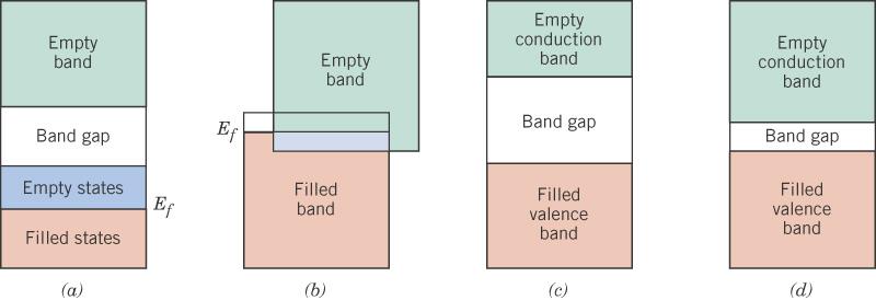
4 Now imagine extending this principle to a Na solid containing Na atoms. In this case, the valence electron orbitals now overlap to form a very large number of closely spaced bands of electron orbitals. Since each of the 3s orbitals in individual Na atoms is only half-filled, the final 3s energy band is only half-filled. Each of these electron orbitals is delocalized throughout the Na solid, being shared among all of the Na atoms. At low room temperature, electrons can easily be thermally excited into unfilled electron orbitals in the upper half of the 3s energy band, allowing them to move in an electric field and conduct current. This corresponds to the situation shown in figure 12.4a. Electrical conductivity in other metals is more complicated. In Mg, the 3s atomic orbital is completely filled, so the 3s energy band is also completely filled in Mg solid. However, this energy band overlaps energetically with another energy band that would otherwise be empty. This allows electrons from one band to be easily thermally excited into the other band, as illustrated in figure 12.4b. Can we understand the electrical behavior of insulators (ceramics) using the same concept of energy bands? This is illustrated in figure 12.4c. In electrically insulating materials, such as most ceramics, the band gap (E g ) is large, so the upper energy band (conduction band) is unoccupied. When the band gap is large compared to thermal energies (kt), then thermal excitation of the conduction band is not feasible, and the material is an electrical insulator. However, in semiconductor materials, E g is relatively small, so there is a small but not insignificant population of electrons in the conduction band, as illustrated in figure 12.4d. As a result, the electrical conductivity of a pure semiconductor is significantly less than that of a pure metal. However, unlike the case of metals, the electrical conductivity of semiconductors can be dramatically altered by changing the temperature or by introducing small amounts of impurities. The latter strategy has led to the development of the modern semiconductor industry. Note that for every electron promoted from the valence to the conduction band, a positively charged electron hole is created in the valence band. These holes serve as positively charged charge carriers.
5 Conductors: In general, materials that are very good electrical conductors predominantly employ electrons as charge carriers. As mentioned above, σ = n e µ where the subscript e refers to electron charge carriers. The resistivity of a metal is increased by any disruption in the regular crystalline lattice, which scatters electrons, as illustrated in Figure e Such disruption can arise from the addition of impurity elements, from deformation associated with cold working, and from an increase in temperature, which both introduces vacancies and causes the atoms to vibrate away from their equilibrium lattice positions. Thus: ρ = ρ + ρ + ρ total t Show figure 12.8, which illustrates all these effects. In essence, all discontinuities in the crystalline lattice reduce the conductivity of metals. For example, since grain boundaries can reflect/deflect electron waves, the electrical conductivity of metals increases as the grain size increases. The increase in resistivity with temperature can be described according to: ρ t = ρ 0 + at where a is the temperature coefficient of resistivity. i d
6 Show figure 12.9, which illustrates the linear relationship between ρ and impurity concentration, at low impurity concentrations. More generally: ρ = Ac 1 where A is a composition-independent constant. i i ( c ) i
7 Example Problem: A tungsten light bulb filament is 9 mm long and 10 µm in diameter. What is the current in the filament when operating at 1000 C with a line voltage of 110 V? Here ρ 0 = -17.5x10⁻⁹ Ω-m and a = 2.48x10⁻¹⁰ Ω-m/ K. Reading this problem carefully, we are really being asked to determine the resistance/resistivity of the tungsten filament at 1000 C. If we know the filament resistance and line voltage, current calculation follows trivially from Ohm s law. We know that: 9 = 0 ρt ρ + at 10 ( 2.48x10 Ω m / K )( 1273 K ) ρ(1000 C ) = 17.5x10 Ω m + ρ 7 ( 1000 C ) = 2.98 x10 Ω m If you instead do this calculation at room temperature, ρ(20 ºC) = 5.51x10⁻⁸ Ω-m. Note that the resistivity is > 5x higher than at room temperature!! Now from Ohm s law and the definition of resistivity: I = V R = VA ρl
8 π 6 2 ( 110 V ) ( 10x10 m) ( 2.98x10 Ω m)( 9x10 m) I = A = Research and Development Example: Cu in Integrated Circuits: Gordon Moore is one of the co-founders of Intel, and he predicted in 1965 that the number of transistors on an integrated circuit would double every two years. This is the now known as Moore s law, and is the economic foundation of the semiconductor industry. Doubling the number of transistors every two years simultaneously yields increasing performance AND decreasing cost. From a manufacturing perspective, Moore s law REQUIRES continuously decreasing device dimensions. In 2011, the semiconductor industry is using the 22 nm node in their most advanced devices. The 1 st Figure below shows a CMOS device schematic. The dimensions of the following materials are all gradually reduced: Gate insulator (SiO 2 here, but new materials under development) Electrical connections to the source, gate and drain (Al, W or Cu) p-type wells below source and drain. These were originally created by diffusion processes, but are now created by ion implantation. Following ion implantation, the damaged Si surface is annealed to activate the p-type dopants. This process involves both diffusion and recrystallization of the damaged Si. Moore s law is illustrated by the two Figures below.


9 In the late 1990 s, Cu began to replace Al as the material for interconnect wires in

10 integrated circuits, or semiconductor devices, including cpu and DRAM chips in computers, chips in home electronics, and chips in communications devices (cell phones, cable modems, etc.). The Figure below shows a CMOS-based integrated circuit from IBM. On the left, all the parallel lines are Cu interconnect wires, like you have seen before in electron microscope images of semiconductor chips. Choosing the best material for the interconnect wires, and choosing the best wiring scheme, have been areas of enormous R&D investment in the semiconductor industry. If you inspect Table 12.1, the two common metals with the lowest ρ are Al and Cu. Ag has the lowest ρ, but is expensive for industrial production, and suffers from electromigration. Originally, Al was used for interconnect wires in computer and other semiconductor chips because it is easier to pattern than Cu, and it is cheaper than the other low-ρ metals. The Al was patterned by depositing a continuous Al film on the wafer surface, and Al was then etched away from the unwanted regions. Eventually, the Al wires had such a small cross-sectional area that their resistance became too high. In addition, the Al wires began to fail by electromigration, where the electron flow causes momentum transfer to Al atoms, eventually forming voids in the Al wires. During the early 1990 s, researchers predicted that Al must eventually be replaced by Cu, and they began to study how to do this. Planning in the semiconductor industry is coordinated through the International Technology Roadmap for Semiconductors (ITRS), Unlike Al, Cu cannot be effectively chemically etched, so new technologies were developed. Cu ionterconnect wires in the above figure were fabricated by a subtractive Damascene process, named for its use in ancient Damascus for making inlaid patterns of precious metals for jewelry. In the Damascene process, the Cu wiring pattern is first etched into an electrical insulator, these trenches are then filled with Cu by electrodeposition, and the excess Cu is polished away by chemical mechanical planarization (CMP). Clarkson has perhaps the world s leading research program in CMP and hosts an international CMP symposium each August in Lake Placid. More information is available online at The Damascene process is shown below:

11 An additional complication of Cu interconnect wiring is that most advanced integrated circuits are multi-level devices. As a result, wire lengths can become very long. This has required the use of fat wiring, shown in the next Figure below, where each successive wiring layer has wires with larger cross-sectional areas. RC circuit delay The networks of resistors and capacitors in integrated circuits have an associated RC circuit delay that limits the speed at which this network can carry electrical signals. This is determined by a mixture of design parameters (dimensions of wires and capacitors) and materials properties (resistivity and dielectric constant): RC = ρ t met ε t met ox ox L 2 In this equation, there are two fundamental material properties, the metal (Cu or Al) resistivity (ρ met ) and is the insulator (SiO 2 or porous replacement) dielectric constant (ε ox ). The other parameters arise from device design, including L (wire length), t met (thickness or width of metal wires), and t ox (thickness or width of dielectric insulator).

12 This illustrates the materials challenges that are created as devices dimensions (t met, t ox ) are continuously reduced according to Moore s law. These reductions in device size cause an increase in the RC time constant. This requires the introduction of metals with lower resistivity (Al replaced by Cu) and dielectric spacing materials with lower dielectric constant (SiO 2 replaced by polymers, then by porous SiO 2 /polymers). Currently, intensive research is ongoing in semiconductor companies into porous low dielectric constant spacer materials. Semiconductor Materials: Many pure solid elements and compounds (Si, Ge, GaAs, InP, etc.) are classified as semiconductors. As discussed in section 12.5, this means that they are intermediate between metals (zero band gap) and insulators (very high band gap). Pure semiconductor materials exhibit relatively low conductivities (still much higher than insulators), but the utility of these materials is that the electrical properties can be modified very dramatically by the introduction of controlled, small amounts of impurities. The properties of some common semiconductor materials are given in Table 12.3 below.
. Electrical current can be carried either by electrons (conduction band) or by electron holes (valence band).")
13 Intrinsic, elemental semiconductors: Pure elemental semiconductors have equal numbers of electrons and electron holes because every electron that is thermally excited to the conduction band leaves behind an electron hole in the valence band. Show figure (at right). Electrical current can be carried either by electrons (conduction band) or by electron holes (valence band). The conduction band electrons are delocalized over the entire crystalline solid, as in metals. However, the valence electrons are associated with specific covalent bonds, so electrical conduction by electron holes requires electrons from an adjacent covalent bond to hop into an empty electron hole. A coordinated series of such hops in the direction of the applied electric field will carry electrical current. The hopping of electrons to fill electron holes is similar to the hopping of atoms to fill vacancies during solid-state diffusion. Although the species moving are actually electrons, this is easier to visualize as hopping of the electron holes in the opposite direction. Therefore, the conductivity of an intrinsic, elemental semiconductor is: σ = n e µ + p e µ where n is the electron concentration, p is the hole concentration, and µ e and µ h are the electron and hole mobility, respectively. However, each thermal activation event produces 1 electron and 1 electron e h
14 hole, so n = p = n i for an intrinsic semiconductor. In addition, the absolute value of the charge carried by each of these carriers is the same: i ( µ ) σ = n e + µ Show Figure below, which illustrates the temperature dependence of the carrier concentration. This is poorly plotted, since it follows an Arrhenius type equation: e h n i exp E g 2kT ln n i E g 2kT The extra factor of occurs 2 in the denominator because 2 charge carriers are created for every thermal excitation. The exponential increase in carrier concentration with temperature causes a corresponding increase in the conductivity with temperature for an intrinsic semiconductor. However, the carrier mobility is typically reduced as the temperature increases, as shown in Figure below. Buried within problem is an equation for the temperature dependence of the conductivity of Ge:
15 σ C T = 3/ 2 exp E g 2kT In general, the contribution of the exponential factor (thermal population of electron-hole pairs) is much greater than the contribution of the T -3/2 factor (reduced mobility with increased temperature), so the latter is sometimes ignored.
16 Example Problem: Starting from an ambient temperature of 300 K, what temperature increase is necessary to double the conductivity of pure Ge? For the sake of simplicity, assume that temperature affects only the carrier concentration, not the electron and hole mobilities. If the only effect of temperature is on the carrier concentration, we can write that: E g σ = σ 0 exp 2kT Take the Arrhenius form of this equation for two temperatures, ambient temperature and that which doubles the conductivity, and divide them: ln2 σ σ ( T ) ( T ) E / 2kT Eg 1 1 g 1 1 σ 0 e 2k T2 T1 = = e Eg / 2kT2 2 σ 0 e σ ln σ ( T ) E ( ) 1 g 1 1 = T2 2k T2 T1 ( ) x10 ev / K K T1 = eV K T = 1.784x T1 = 317 K / K Notice that the conductivity doubles from only a 17ºK rise in temperature. If we take into account the possible T -3/2 factor, then this problem can only be solved by trial and error. In many cases, it is easier to include only the exponential factor, and the answer that is obtained is still reasonably accurate. Note here that(317/300) -1.5 = 0.92, so this effect is much smaller than the exponential effect due to carrier concentration. Extrinsic, elemental semiconductors: Extrinsic semiconductors are formed by deliberate addition of specific impurity elements (dopants) to a pure semiconductor material. The addition of Group V elements, which have one extra valence electron than Si and Ge, creates n-type semiconductors. Four of the five electrons in Group V elements (P, As, Sb) are used to create local bonds to 1


17 adjacent Si atoms. The 5 th electron is not needed for bonding and produces a donor level near the conduction band, which is much easier to thermally activate into the conduction band than valence electrons. Show figure (at right). The result is that electrons far outnumber electron holes, and the conductivity of an n- type semiconductor is: σ = n e µ The addition of Group III elements, which have one less valence electron than Si and Ge, creates p-type semiconductors. All three electrons in Group III elements (Al, Ga, In) are used to create local bonds to adjacent Si atoms, but four bonds are needed to adjacent Si atoms. This results in the creation of an acceptor level near the valence band of Si, as shown in figure below, that is relatively easy to thermally populate from the valence band. The result is that electron holes far outnumber electrons, and the conductivity of a p- type semiconductor is: σ = p e µ Discuss qualitatively the dependence of carrier concentration on temperature, and the factors that influence carrier mobility. Show figure (on next page). e h
18 Effect of dopant concentration on electrical conductivity: Here is a simple model calculation to illustrate how dramatically the addition of dopant elements increases the electrical conductivity of Si, and other semiconductors. The electron concentration (n) in an n-type semiconductor is roughly equal to the concentration of n-type doping elements that are added. Therefore, we can calculate the increase in conductivity with the concentration of n-type dopant. For intrinsic (pure) Si at room temperature, Table 12.3 gives the room-temperature conductivity (σ) as 4x10⁻⁴ (Ω-m) -1. With addition of atom% As, assuming that all the extra electrons are activated into the conduction band: 8 atoms 8 atoms n Si = = = 3 3 a 8R R 3 n Si = 4.94x10 3 = m 64 9 ( 0.118x10 m)
19 For atom% As, n As ( 4.94x10 m ) = 4.94x10 5 = m Looking up the electron mobility from Table 12.3: σ = σ = n e µ ( 4.94x10 m )( 1.602x10 C )( m / V sec) e σ = 1.1x10 Ω m A small level of impurity (0.001 atom%) increases the conductivity by 8 orders of magnitude!! The ability to tune the electrical properties of semiconductors is what makes semiconductor devices possible. We have not considered whether or not As is sufficiently soluble in Si. Does it have the same crystal structure, similar atomic radius, similar valance and electronegativity? As almost certainly fails this test, but this does not matter, given the low concentration (0.001 atom%) of As. If you inspect any of the phase diagrams in Chapter 10, the solubility limit of even relatively insoluble materials is usually not below atom%. How do transistors work? In the 21 st century, one might argue that all educated people should understand how a transistor works. The main components of a transistor are p-n junctions, which are typically rectifying, meaning that they behave like diodes, carrying current in one direction only. A p-n junction is a region where a p-type semiconductor borders with an n-semiconductor. This is illustrated schematically in Figure of the textbook below.

20 Under a forward bias, electrons are repelled from the negative terminal and attracted by the positive terminal, directing them through the p-n junction. Holes experience the opposite forces, but are also directed through the p-n junction. On the other hand, under reverse bias, electrons and holes are both drawn away from the p-n junction, leaving this region bereft of charge carriers. As a result, the p-n junction is only conductive under forward bias, so its i-v behavior is shown in Figure below. The p-n junction behaves like a diode (rectifier), not a resistor.
 wells to form a p-channel (n-channel) MOSFET.")
21 Most transistors are now metal oxide semiconductor field effect transistors (MOSFET), as shown in Figure below, p-channel MOSFET device. In a MOSFET, two p-n junctions of opposite polarity are created by forming two p-doped (n-doped) wells to form a p-channel (n-channel) MOSFET. In either case, the material between the two wells that are formed contains dopant of the opposite type. Since the two p-n junctions are of opposite polarity, the transistor will not carry current when it is off. In other words, if no potential is applied to the gate, the resistance between the source and drain is quite high for an applied voltage of either polarity. However, if a
22 large enough negative potential is applied to the gate electrode of a p-channel device, the negative potential can penetrate through the thin gate dielectric, repelling electrons from the region near the gate. This creates a thin channel near the gate that the applied potential has converted from n-type to p-type. The p-channel region that is formed creates a continuous p-type pathway between the source and drain. Now the transistor is conducting, and current can flow between the source and drain. This is a simple method fro making a binary switch (logic gate), or an amplifier. By connecting many transistors in a logic circuit, complicated integrated circuits can be fabricated. Note that the transistor shown in Figure is fabricated by surface engineering. The n-type Si substrate is about 1 mm thick, but the p-type dopant wells are about 100 nm deep, and the gate oxide is perhaps 1-2 nm thick. Most of the thickness of the Si wafer is not involved in the actual transistor, but provides mechanical support so that the transistor is not broken easily. Traditionally, the p-type dopant wells were created by diffusion of p-type dopants (Al, Ga, In) inside the Si wafer. As we learned in Chapter 6, diffusion over a 100 nm length scale is much more rapid than diffusion over a 1 mm length scale, illustrating why the transistor is created only in the surface layer. Diffusion has been gradually replaced by ion implantation for many applications, since this allows better control over the exact distribution of the dopant element within the Si wafer. For more information about CMOS transistors and how they work, see the information available at and See, for example:
ESE370: Circuit-Level Modeling, Design, and Optimization for Digital Systems
 ESE370: Circuit-Level Modeling, Design, and Optimization for Digital Systems Lec 6: September 14, 2015 MOS Model You are Here: Transistor Edition! Previously: simple models (0 and 1 st order) " Comfortable
A semiconductor is an almost insulating material, in which by contamination (doping) positive or negative charge carriers can be introduced.
 positive or negative charge carriers can be introduced.") Semiconductor A semiconductor is an almost insulating material, in which by contamination (doping) positive or negative charge carriers can be introduced. Page 2 Semiconductor materials Page 3 Energy levels
Semiconductor A semiconductor is an almost insulating material, in which by contamination (doping) positive or negative charge carriers can be introduced. Page 2 Semiconductor materials Page 3 Energy levels
ISSUES TO ADDRESS...
 Chapter 12: Electrical Properties School of Mechanical Engineering Choi, Hae-Jin Materials Science - Prof. Choi, Hae-Jin Chapter 12-1 ISSUES TO ADDRESS... How are electrical conductance and resistance
EE130: Integrated Circuit Devices
 EE130: Integrated Circuit Devices (online at http://webcast.berkeley.edu) Instructor: Prof. Tsu-Jae King (tking@eecs.berkeley.edu) TA s: Marie Eyoum (meyoum@eecs.berkeley.edu) Alvaro Padilla (apadilla@eecs.berkeley.edu)
ESE370: Circuit-Level Modeling, Design, and Optimization for Digital Systems
 ESE370: Circuit-Level Modeling, Design, and Optimization for Digital Systems Lec 6: September 18, 2017 MOS Model You are Here: Transistor Edition! Previously: simple models (0 and 1 st order) " Comfortable
ESE370: Circuit-Level Modeling, Design, and Optimization for Digital Systems. Today MOS MOS. Capacitor. Idea
 ESE370: Circuit-Level Modeling, Design, and Optimization for Digital Systems Day 9: September 26, 2011 MOS Model Today MOS Structure Basic Idea Semiconductor Physics Metals, insulators Silicon lattice
12/10/09. Chapter 18: Electrical Properties. View of an Integrated Circuit. Electrical Conduction ISSUES TO ADDRESS...
 Chapter 18: Electrical Properties ISSUES TO ADDRESS... How are electrical conductance and resistance characterized? What are the physical phenomena that distinguish? For metals, how is affected by and
! Previously: simple models (0 and 1 st order) " Comfortable with basic functions and circuits. ! This week and next (4 lectures)
 Comfortable with basic functions and circuits. ! This week and next (4 lectures)") ESE370: CircuitLevel Modeling, Design, and Optimization for Digital Systems Lec 6: September 14, 2015 MOS Model You are Here: Transistor Edition! Previously: simple models (0 and 1 st order) " Comfortable
ESE370: CircuitLevel Modeling, Design, and Optimization for Digital Systems Lec 6: September 14, 2015 MOS Model You are Here: Transistor Edition! Previously: simple models (0 and 1 st order) " Comfortable
Review of Semiconductor Fundamentals
 ECE 541/ME 541 Microelectronic Fabrication Techniques Review of Semiconductor Fundamentals Zheng Yang (ERF 3017, email: yangzhen@uic.edu) Page 1 Semiconductor A semiconductor is an almost insulating material,
FREQUENTLY ASKED QUESTIONS February 21, 2017
 FREQUENTLY ASKED QUESTIONS February 21, 2017 Content Questions How do you place a single arsenic atom with the ratio 1 in 100 million? Sounds difficult to get evenly spread throughout. Yes, techniques
Lecture 7: Extrinsic semiconductors - Fermi level
 Lecture 7: Extrinsic semiconductors - Fermi level Contents 1 Dopant materials 1 2 E F in extrinsic semiconductors 5 3 Temperature dependence of carrier concentration 6 3.1 Low temperature regime (T < T
Semiconductors. Semiconductors also can collect and generate photons, so they are important in optoelectronic or photonic applications.
 Semiconductors Semiconducting materials have electrical properties that fall between true conductors, (like metals) which are always highly conducting and insulators (like glass or plastic or common ceramics)
! Previously: simple models (0 and 1 st order) " Comfortable with basic functions and circuits. ! This week and next (4 lectures)
 Comfortable with basic functions and circuits. ! This week and next (4 lectures)") ESE370: CircuitLevel Modeling, Design, and Optimization for Digital Systems Lec 6: September 18, 2017 MOS Model You are Here: Transistor Edition! Previously: simple models (0 and 1 st order) " Comfortable
ESE370: CircuitLevel Modeling, Design, and Optimization for Digital Systems Lec 6: September 18, 2017 MOS Model You are Here: Transistor Edition! Previously: simple models (0 and 1 st order) " Comfortable
ESE 570: Digital Integrated Circuits and VLSI Fundamentals
 ESE 570: Digital Integrated Circuits and VLSI Fundamentals Lec 4: January 23, 2018 MOS Transistor Theory, MOS Model Penn ESE 570 Spring 2018 Khanna Lecture Outline! CMOS Process Enhancements! Semiconductor
EE301 Electronics I , Fall
 EE301 Electronics I 2018-2019, Fall 1. Introduction to Microelectronics (1 Week/3 Hrs.) Introduction, Historical Background, Basic Consepts 2. Rewiev of Semiconductors (1 Week/3 Hrs.) Semiconductor materials
CME 300 Properties of Materials. ANSWERS: Homework 9 November 26, As atoms approach each other in the solid state the quantized energy states:
 CME 300 Properties of Materials ANSWERS: Homework 9 November 26, 2011 As atoms approach each other in the solid state the quantized energy states: are split. This splitting is associated with the wave
ESE 570: Digital Integrated Circuits and VLSI Fundamentals
 ESE 570: Digital Integrated Circuits and VLSI Fundamentals Lec 4: January 29, 2019 MOS Transistor Theory, MOS Model Penn ESE 570 Spring 2019 Khanna Lecture Outline! CMOS Process Enhancements! Semiconductor
CLASS 12th. Semiconductors
 CLASS 12th Semiconductors 01. Distinction Between Metals, Insulators and Semi-Conductors Metals are good conductors of electricity, insulators do not conduct electricity, while the semiconductors have
Classification of Solids
 Classification of Solids Classification by conductivity, which is related to the band structure: (Filled bands are shown dark; D(E) = Density of states) Class Electron Density Density of States D(E) Examples
EE 5211 Analog Integrated Circuit Design. Hua Tang Fall 2012
 EE 5211 Analog Integrated Circuit Design Hua Tang Fall 2012 Today s topic: 1. Introduction to Analog IC 2. IC Manufacturing (Chapter 2) Introduction What is Integrated Circuit (IC) vs discrete circuits?
Introduction to Engineering Materials ENGR2000. Dr.Coates
 Introduction to Engineering Materials ENGR2000 Chapter 18: Electrical Properties Dr.Coates 18.2 Ohm s Law V = IR where R is the resistance of the material, V is the voltage and I is the current. l R A
Electro - Principles I
 Electro - Principles I Page 10-1 Atomic Theory It is necessary to know what goes on at the atomic level of a semiconductor so the characteristics of the semiconductor can be understood. In many cases a
Mat E 272 Lecture 25: Electrical properties of materials
 Mat E 272 Lecture 25: Electrical properties of materials December 6, 2001 Introduction: Calcium and copper are both metals; Ca has a valence of +2 (2 electrons per atom) while Cu has a valence of +1 (1
Introduction to Semiconductor Physics. Prof.P. Ravindran, Department of Physics, Central University of Tamil Nadu, India
 Introduction to Semiconductor Physics 1 Prof.P. Ravindran, Department of Physics, Central University of Tamil Nadu, India http://folk.uio.no/ravi/cmp2013 Review of Semiconductor Physics Semiconductor fundamentals
Chapter 1 Overview of Semiconductor Materials and Physics
 Chapter 1 Overview of Semiconductor Materials and Physics Professor Paul K. Chu Conductivity / Resistivity of Insulators, Semiconductors, and Conductors Semiconductor Elements Period II III IV V VI 2 B
Lecture 2. Semiconductor Physics. Sunday 4/10/2015 Semiconductor Physics 1-1
 Lecture 2 Semiconductor Physics Sunday 4/10/2015 Semiconductor Physics 1-1 Outline Intrinsic bond model: electrons and holes Charge carrier generation and recombination Intrinsic semiconductor Doping:
! CMOS Process Enhancements. ! Semiconductor Physics. " Band gaps. " Field Effects. ! MOS Physics. " Cut-off. " Depletion.
 ESE 570: Digital Integrated Circuits and VLSI Fundamentals Lec 4: January 9, 019 MOS Transistor Theory, MOS Model Lecture Outline CMOS Process Enhancements Semiconductor Physics Band gaps Field Effects
Chapter 4: Bonding in Solids and Electronic Properties. Free electron theory
 Chapter 4: Bonding in Solids and Electronic Properties Free electron theory Consider free electrons in a metal an electron gas. regards a metal as a box in which electrons are free to move. assumes nuclei
! CMOS Process Enhancements. ! Semiconductor Physics. " Band gaps. " Field Effects. ! MOS Physics. " Cut-off. " Depletion.
 ESE 570: Digital Integrated Circuits and VLSI Fundamentals Lec 4: January 3, 018 MOS Transistor Theory, MOS Model Lecture Outline! CMOS Process Enhancements! Semiconductor Physics " Band gaps " Field Effects!
Lecture 1. OUTLINE Basic Semiconductor Physics. Reading: Chapter 2.1. Semiconductors Intrinsic (undoped) silicon Doping Carrier concentrations
 silicon Doping Carrier concentrations") Lecture 1 OUTLINE Basic Semiconductor Physics Semiconductors Intrinsic (undoped) silicon Doping Carrier concentrations Reading: Chapter 2.1 EE105 Fall 2007 Lecture 1, Slide 1 What is a Semiconductor? Low
Lecture 1 OUTLINE Basic Semiconductor Physics Semiconductors Intrinsic (undoped) silicon Doping Carrier concentrations Reading: Chapter 2.1 EE105 Fall 2007 Lecture 1, Slide 1 What is a Semiconductor? Low
Chemistry Instrumental Analysis Lecture 8. Chem 4631
 Chemistry 4631 Instrumental Analysis Lecture 8 UV to IR Components of Optical Basic components of spectroscopic instruments: stable source of radiant energy transparent container to hold sample device
Electronics The basics of semiconductor physics
 Electronics The basics of semiconductor physics Prof. Márta Rencz, Gergely Nagy BME DED September 16, 2013 The basic properties of semiconductors Semiconductors conductance is between that of conductors
Section 12: Intro to Devices
 Section 12: Intro to Devices Extensive reading materials on reserve, including Robert F. Pierret, Semiconductor Device Fundamentals Bond Model of Electrons and Holes Si Si Si Si Si Si Si Si Si Silicon
Crystal Properties. MS415 Lec. 2. High performance, high current. ZnO. GaN
 Crystal Properties Crystal Lattices: Periodic arrangement of atoms Repeated unit cells (solid-state) Stuffing atoms into unit cells Determine mechanical & electrical properties High performance, high current
Unit IV Semiconductors Engineering Physics
 Introduction A semiconductor is a material that has a resistivity lies between that of a conductor and an insulator. The conductivity of a semiconductor material can be varied under an external electrical
Lecture 0: Introduction
 Lecture 0: Introduction Introduction q Integrated circuits: many transistors on one chip q Very Large Scale Integration (VLSI): bucketloads! q Complementary Metal Oxide Semiconductor Fast, cheap, low power
LECTURE 23. MOS transistor. 1 We need a smart switch, i.e., an electronically controlled switch. Lecture Digital Circuits, Logic
 LECTURE 23 Lecture 16-20 Digital Circuits, Logic 1 We need a smart switch, i.e., an electronically controlled switch 2 We need a gain element for example, to make comparators. The device of our dreams
Semiconductors 1. Explain different types of semiconductors in detail with necessary bond diagrams. Intrinsic semiconductors:
 Semiconductors 1. Explain different types of semiconductors in detail with necessary bond diagrams. There are two types of semi conductors. 1. Intrinsic semiconductors 2. Extrinsic semiconductors Intrinsic
Digital Electronics Part II - Circuits
 Digital Electronics Part - Circuits Dr.. J. Wassell Gates from Transistors ntroduction Logic circuits are non-linear, consequently we will introduce a graphical technique for analysing such circuits The
ELEMENTARY BAND THEORY
 ELEMENTARY BAND THEORY PHYSICIST Solid state band Valence band, VB Conduction band, CB Fermi energy, E F Bloch orbital, delocalized n-doping p-doping Band gap, E g Direct band gap Indirect band gap Phonon
Introduction to Semiconductor Devices
 Physics 233 Experiment 48 Introduction to Semiconductor Devices References 1. G.W. Neudeck, The PN Junction Diode, Addison-Wesley MA 1989 2. Background notes (Appendix A) 3. Specification sheet for Diode
Self-study problems and questions Processing and Device Technology, FFF110/FYSD13
 Self-study problems and questions Processing and Device Technology, FFF110/FYSD13 Version 2016_01 In addition to the problems discussed at the seminars and at the lectures, you can use this set of problems
ESE 570: Digital Integrated Circuits and VLSI Fundamentals
 ESE 570: Digital Integrated Circuits and VLSI Fundamentals Lec 4: January 24, 2017 MOS Transistor Theory, MOS Model Penn ESE 570 Spring 2017 Khanna Lecture Outline! Semiconductor Physics " Band gaps "
Semiconductor Detectors
 Semiconductor Detectors Summary of Last Lecture Band structure in Solids: Conduction band Conduction band thermal conductivity: E g > 5 ev Valence band Insulator Charge carrier in conductor: e - Charge
Chap. 1 (Introduction), Chap. 2 (Components and Circuits)
, Chap. 2 (Components and Circuits)") CHEM 455 The class describes the principles and applications of modern analytical instruments. Emphasis is placed upon the theoretical basis of each type of instrument, its optimal area of application,
CHEM 455 The class describes the principles and applications of modern analytical instruments. Emphasis is placed upon the theoretical basis of each type of instrument, its optimal area of application,
Semiconductor Physics
 Semiconductor Physics Motivation Is it possible that there might be current flowing in a conductor (or a semiconductor) even when there is no potential difference supplied across its ends? Look at the
Introduction to Semiconductor Devices
 Physics 233 Experiment 48 Introduction to Semiconductor Devices References 1. G.W. Neudeck, The PN Junction Diode, Addison-Wesley MA 1989 2. Background notes (Appendix A) 3. Specification sheet for Diode
ECE 250 Electronic Devices 1. Electronic Device Modeling
 ECE 250 Electronic Devices 1 ECE 250 Electronic Device Modeling ECE 250 Electronic Devices 2 Introduction to Semiconductor Physics You should really take a semiconductor device physics course. We can only
Session 0: Review of Solid State Devices. From Atom to Transistor
 Session 0: Review of Solid State Devices From Atom to Transistor 1 Objective To Understand: how Diodes, and Transistors operate! p n p+ n p- n+ n+ p 2 21 Century Alchemy! Ohm s law resistivity Resistivity
Semiconductor Detectors are Ionization Chambers. Detection volume with electric field Energy deposited positive and negative charge pairs
 1 V. Semiconductor Detectors V.1. Principles Semiconductor Detectors are Ionization Chambers Detection volume with electric field Energy deposited positive and negative charge pairs Charges move in field
First-Hand Investigation: Modeling of Semiconductors
 perform an investigation to model the behaviour of semiconductors, including the creation of a hole or positive charge on the atom that has lost the electron and the movement of electrons and holes in
Section 12: Intro to Devices
 Section 12: Intro to Devices Extensive reading materials on reserve, including Robert F. Pierret, Semiconductor Device Fundamentals EE143 Ali Javey Bond Model of Electrons and Holes Si Si Si Si Si Si Si
Nanoelectronics. Topics
 Nanoelectronics Topics Moore s Law Inorganic nanoelectronic devices Resonant tunneling Quantum dots Single electron transistors Motivation for molecular electronics The review article Overview of Nanoelectronic
Semiconductor physics I. The Crystal Structure of Solids
 Lecture 3 Semiconductor physics I The Crystal Structure of Solids 1 Semiconductor materials Types of solids Space lattices Atomic Bonding Imperfection and doping in SOLIDS 2 Semiconductor Semiconductors
Semiconductor Device Physics
 1 Semiconductor Device Physics Lecture 1 http://zitompul.wordpress.com 2 0 1 3 2 Semiconductor Device Physics Textbook: Semiconductor Device Fundamentals, Robert F. Pierret, International Edition, Addison
ELECTRONIC I Lecture 1 Introduction to semiconductor. By Asst. Prof Dr. Jassim K. Hmood
 ELECTRONIC I Lecture 1 Introduction to semiconductor By Asst. Prof Dr. Jassim K. Hmood SOLID-STATE ELECTRONIC MATERIALS Electronic materials generally can be divided into three categories: insulators,
EECS143 Microfabrication Technology
 EECS143 Microfabrication Technology Professor Ali Javey Introduction to Materials Lecture 1 Evolution of Devices Yesterday s Transistor (1947) Today s Transistor (2006) Why Semiconductors? Conductors e.g
Semiconductor Physics Problems 2015
 Semiconductor Physics Problems 2015 Page and figure numbers refer to Semiconductor Devices Physics and Technology, 3rd edition, by SM Sze and M-K Lee 1. The purest semiconductor crystals it is possible
smal band gap Saturday, April 9, 2011
 small band gap upper (conduction) band empty small gap valence band filled 2s 2p 2s 2p hybrid (s+p)band 2p no gap 2s (depend on the crystallographic orientation) extrinsic semiconductor semi-metal electron
Semi-Conductors insulators semi-conductors N-type Semi-Conductors P-type Semi-Conductors
 Semi-Conductors In the metal materials considered earlier, the coupling of the atoms together to form the material decouples an electron from each atom setting it free to roam around inside the material.
3.1 Introduction to Semiconductors. Y. Baghzouz ECE Department UNLV
 3.1 Introduction to Semiconductors Y. Baghzouz ECE Department UNLV Introduction In this lecture, we will cover the basic aspects of semiconductor materials, and the physical mechanisms which are at the
Fabrication Technology, Part I
 EEL5225: Principles of MEMS Transducers (Fall 2004) Fabrication Technology, Part I Agenda: Microfabrication Overview Basic semiconductor devices Materials Key processes Oxidation Thin-film Deposition Reading:
Engineering 2000 Chapter 8 Semiconductors. ENG2000: R.I. Hornsey Semi: 1
 Engineering 2000 Chapter 8 Semiconductors ENG2000: R.I. Hornsey Semi: 1 Overview We need to know the electrical properties of Si To do this, we must also draw on some of the physical properties and we
V = IR or R = V I. R = ρ l A
 Metals and Semiconductors Ram Seshadri MRL 2031, x6129, seshadri@mrl.ucsb.edu Electrical resistance and Ohm s Law: If an electric current I (units of A, Ampère) flows through a conductor with resistance
3C3 Analogue Circuits
 Department of Electronic & Electrical Engineering Trinity College Dublin, 2014 3C3 Analogue Circuits Prof J K Vij jvij@tcd.ie Lecture 1: Introduction/ Semiconductors & Doping 1 Course Outline (subject
Resistance (R) Temperature (T)
 Temperature (T)") CHAPTER 1 Physical Properties of Elements and Semiconductors 1.1 Introduction Semiconductors constitute a large class of substances which have resistivities lying between those of insulators and conductors.
CHAPTER 1 Physical Properties of Elements and Semiconductors 1.1 Introduction Semiconductors constitute a large class of substances which have resistivities lying between those of insulators and conductors.
CLASS 1 & 2 REVISION ON SEMICONDUCTOR PHYSICS. Reference: Electronic Devices by Floyd
 CLASS 1 & 2 REVISION ON SEMICONDUCTOR PHYSICS Reference: Electronic Devices by Floyd 1 ELECTRONIC DEVICES Diodes, transistors and integrated circuits (IC) are typical devices in electronic circuits. All
Lecture 2. Introduction to semiconductors Structures and characteristics in semiconductors
 Lecture 2 Introduction to semiconductors Structures and characteristics in semiconductors Semiconductor p-n junction Metal Oxide Silicon structure Semiconductor contact Literature Glen F. Knoll, Radiation
Chapter 3 Basics Semiconductor Devices and Processing
 Chapter 3 Basics Semiconductor Devices and Processing Hong Xiao, Ph. D. www2.austin.cc.tx.us/hongxiao/book.htm Hong Xiao, Ph. D. www2.austin.cc.tx.us/hongxiao/book.htm 1 Objectives Identify at least two
collisions of electrons. In semiconductor, in certain temperature ranges the conductivity increases rapidly by increasing temperature
 1.9. Temperature Dependence of Semiconductor Conductivity Such dependence is one most important in semiconductor. In metals, Conductivity decreases by increasing temperature due to greater frequency of
Electronic Devices & Circuits
 Electronic Devices & Circuits For Electronics & Communication Engineering By www.thegateacademy.com Syllabus Syllabus for Electronic Devices Energy Bands in Intrinsic and Extrinsic Silicon, Carrier Transport,
Semiconductors. SEM and EDAX images of an integrated circuit. SEM EDAX: Si EDAX: Al. Institut für Werkstoffe der ElektrotechnikIWE
 SEM and EDAX images of an integrated circuit SEM EDAX: Si EDAX: Al source: [Cal 99 / 605] M&D-.PPT, slide: 1, 12.02.02 Classification semiconductors electronic semiconductors mixed conductors ionic conductors
ITT Technical Institute ET215 Devices I Unit 1
 ITT Technical Institute ET215 Devices I Unit 1 Chapter 1 Chapter 2, Sections 2.1-2.4 Chapter 1 Basic Concepts of Analog Circuits Recall ET115 & ET145 Ohms Law I = V/R If voltage across a resistor increases
Physical Properties of Materials. 1. Electrical Properties 2. Optical Properties 3. Magnetic Properties
 Physical Properties of Materials 1. Electrical Properties 2. Optical Properties 3. Magnetic Properties 1 1. electrical properties 2 (1) electrical conduction in metals classical Model metallic bonds make
GaN based transistors
 GaN based transistors S FP FP dielectric G SiO 2 Al x Ga 1-x N barrier i-gan Buffer i-sic D Transistors "The Transistor was probably the most important invention of the 20th Century The American Institute
ECE 142: Electronic Circuits Lecture 3: Semiconductors
 Faculty of Engineering ECE 142: Electronic Circuits Lecture 3: Semiconductors Agenda Intrinsic Semiconductors Extrinsic Semiconductors N-type P-type Carrier Transport Drift Diffusion Semiconductors A semiconductor
Lecture Outline. ESE 570: Digital Integrated Circuits and VLSI Fundamentals. Review: MOSFET N-Type, P-Type. Semiconductor Physics.
 ESE 57: Digital Integrated Circuits and VLSI Fundamentals Lec 4: January 24, 217 MOS Transistor Theory, MOS Model Lecture Outline! Semiconductor Physics " Band gaps " Field Effects! MOS Physics " Cutoff
Microscopic Ohm s Law
 Microscopic Ohm s Law Outline Semiconductor Review Electron Scattering and Effective Mass Microscopic Derivation of Ohm s Law 1 TRUE / FALSE 1. Judging from the filled bands, material A is an insulator.
Ga and P Atoms to Covalent Solid GaP
 Ga and P Atoms to Covalent Solid GaP Band Gaps in Binary Group III-V Semiconductors Mixed Semiconductors Affect of replacing some of the As with P in GaAs Band Gap (ev) (nm) GaAs 1.35 919 (IR) GaP 2.24
MSE 310/ECE 340: Electrical Properties of Materials Fall 2014 Department of Materials Science and Engineering Boise State University
 MSE 310/ECE 340: Electrical Properties of Materials Fall 2014 Department of Materials Science and Engineering Boise State University Practice Final Exam 1 Read the questions carefully Label all figures
Lecture 2. Introduction to semiconductors Structures and characteristics in semiconductors
 Lecture 2 Introduction to semiconductors Structures and characteristics in semiconductors Semiconductor p-n junction Metal Oxide Silicon structure Semiconductor contact Literature Glen F. Knoll, Radiation
SEMICONDUCTORS. Conductivity lies between conductors and insulators. The flow of charge in a metal results from the
 SEMICONDUCTORS Conductivity lies between conductors and insulators The flow of charge in a metal results from the movement of electrons Electros are negatively charged particles (q=1.60x10⁻¹⁹ C ) The outermost
Calculating Band Structure
 Calculating Band Structure Nearly free electron Assume plane wave solution for electrons Weak potential V(x) Brillouin zone edge Tight binding method Electrons in local atomic states (bound states) Interatomic
EECS130 Integrated Circuit Devices
 EECS130 Integrated Circuit Devices Professor Ali Javey 8/30/2007 Semiconductor Fundamentals Lecture 2 Read: Chapters 1 and 2 Last Lecture: Energy Band Diagram Conduction band E c E g Band gap E v Valence
Quiz #1 Practice Problem Set
 Name: Student Number: ELEC 3908 Physical Electronics Quiz #1 Practice Problem Set? Minutes January 22, 2016 - No aids except a non-programmable calculator - All questions must be answered - All questions
KATIHAL FİZİĞİ MNT-510
 KATIHAL FİZİĞİ MNT-510 YARIİLETKENLER Kaynaklar: Katıhal Fiziği, Prof. Dr. Mustafa Dikici, Seçkin Yayıncılık Katıhal Fiziği, Şakir Aydoğan, Nobel Yayıncılık, Physics for Computer Science Students: With
Lecture 3b. Bonding Model and Dopants. Reading: (Cont d) Notes and Anderson 2 sections
 Notes and Anderson 2 sections") Lecture 3b Bonding Model and Dopants Reading: (Cont d) Notes and Anderson 2 sections 2.3-2.7 The need for more control over carrier concentration Without help the total number of carriers (electrons and
Lecture 3b Bonding Model and Dopants Reading: (Cont d) Notes and Anderson 2 sections 2.3-2.7 The need for more control over carrier concentration Without help the total number of carriers (electrons and
Free Electron Model for Metals
 Free Electron Model for Metals Metals are very good at conducting both heat and electricity. A lattice of in a sea of electrons shared between all nuclei (moving freely between them): This is referred
EXTRINSIC SEMICONDUCTOR
 EXTRINSIC SEMICONDUCTOR In an extrinsic semiconducting material, the charge carriers originate from impurity atoms added to the original material is called impurity [or] extrinsic semiconductor. This Semiconductor
Ch. 2: Energy Bands And Charge Carriers In Semiconductors
 Ch. 2: Energy Bands And Charge Carriers In Semiconductors Discrete energy levels arise from balance of attraction force between electrons and nucleus and repulsion force between electrons each electron
EE143 Fall 2016 Microfabrication Technologies. Evolution of Devices
 EE143 Fall 2016 Microfabrication Technologies Prof. Ming C. Wu wu@eecs.berkeley.edu 511 Sutardja Dai Hall (SDH) 1-1 Evolution of Devices Yesterday s Transistor (1947) Today s Transistor (2006) 1-2 1 Why
Electrical Properties
 Electrical Properties Electrical Conduction R Ohm s law V = IR I l Area, A V where I is current (Ampere), V is voltage (Volts) and R is the resistance (Ohms or ) of the conductor Resistivity Resistivity,
EE 446/646 Photovoltaic Devices I. Y. Baghzouz
 EE 446/646 Photovoltaic Devices I Y. Baghzouz What is Photovoltaics? First used in about 1890, the word has two parts: photo, derived from the Greek word for light, volt, relating to electricity pioneer
Junction Diodes. Tim Sumner, Imperial College, Rm: 1009, x /18/2006
 Junction Diodes Most elementary solid state junction electronic devices. They conduct in one direction (almost correct). Useful when one converts from AC to DC (rectifier). But today diodes have a wide
ELECTRONIC DEVICES AND CIRCUITS SUMMARY
 ELECTRONIC DEVICES AND CIRCUITS SUMMARY Classification of Materials: Insulator: An insulator is a material that offers a very low level (or negligible) of conductivity when voltage is applied. Eg: Paper,
Lecture 20: Semiconductor Structures Kittel Ch 17, p , extra material in the class notes
 Lecture 20: Semiconductor Structures Kittel Ch 17, p 494-503, 507-511 + extra material in the class notes MOS Structure Layer Structure metal Oxide insulator Semiconductor Semiconductor Large-gap Semiconductor
MOSFET: Introduction
 E&CE 437 Integrated VLSI Systems MOS Transistor 1 of 30 MOSFET: Introduction Metal oxide semiconductor field effect transistor (MOSFET) or MOS is widely used for implementing digital designs Its major
EE495/695 Introduction to Semiconductors I. Y. Baghzouz ECE Department UNLV
 EE495/695 Introduction to Semiconductors I Y. Baghzouz ECE Department UNLV Introduction Solar cells have always been aligned closely with other electronic devices. We will cover the basic aspects of semiconductor
n N D n p = n i p N A
 Summary of electron and hole concentration in semiconductors Intrinsic semiconductor: E G n kt i = pi = N e 2 0 Donor-doped semiconductor: n N D where N D is the concentration of donor impurity Acceptor-doped
Higher Physics. Electricity. Summary Notes. Monitoring and measuring a.c. Current, potential difference, power and resistance
 Higher Physics Electricity Summary Notes Monitoring and measuring a.c. Current, potential difference, power and resistance Electrical sources and internal resistance Capacitors Conductors, semiconductors