Band Alignment and Graded Heterostructures. Guofu Niu Auburn University
|
|
|
- Stella Bates
- 6 years ago
- Views:
Transcription
1 Band Alignment and Graded Heterostructures Guofu Niu Auburn University
2 Outline Concept of electron affinity Types of heterojunction band alignment Band alignment in strained SiGe/Si Cusps and Notches at heterojunction Graded bandgap Impact of doping on equilibrium band diagram in graded heterostructures
3 Reference My own SiGe book more on npn SiGe HBT base grading The proc. Of the IEEE review paper by Nobel physics winner Herb Kromer part of this lecture material came from that paper The book chapter of Prof. Schubert of RPI book can be downloaded online from docstoc.com n.tex - by Alfreov, who shared the noble physics prize with Kroemer for heterostructure laser work 3
4 Band alignment So far I have intentionally avoided the issue of band alignment at heterojunction interface We have simply focused on ni^2 change due to bandgap change for abrupt junction Ec or Ev gradient produced by Ge grading We have seen in our Sdevice simulation that the final band diagrams actually depend on doping A Ec gradient favorable for electron transport is obtained for forward Ge grading in p-type (npn HBT) A Ev gradient favorable for hole transport is obtained for forward Ge grading in n-type (pnp HBT)


5 Electron Affinity rough picture Neglect interface between vacuum and semiconductor, vacuum level is drawn to be position independent The energy needed to move an electron from Ec to vacuum level is called electron affinity. 5
6 Electron Affinity Model The electron affinity model is the oldest model invoked to calculate the band offsets in semiconductor heterostructures (Anderson, 1962). This model has proven to give accurate predictions for the band offsets in several semiconductor heterostructures, whereas the model fails for others. We first outline the basic idea of the electron affinity model and then discuss the limitations of this model. 6

7 Semiconductor vacuum interface The band diagram of a semiconductor-vacuum interface is shown. Near the surface, the n-type semiconductor is depleted of free electrons due to the pinning of the Fermi level near the middle of the forbidden gap at the semiconductor surface. Such a pinning of the Fermi level at the surface occurs for most semiconductors. The energy required to move an electron from the semiconductor to the vacuum surrounding the semiconductor depends on the initial energy of the electron in the semiconductor. Promoting an electron from the bottom of the conduction band to the vacuum beyond the reach of image forces requires work called the Electron Affinity. Lifting an electron from the Fermi level requires work called the Work Function, which is defined the same way in semiconductors as it is in metals. Finally, raising an electron from the top of the valence band requires the ionization energy. 7

8 Interface of Two Semiconductors Next consider that two semiconductors are brought into physical contact. The two semiconductors are assumed to have an electron affinity of chi1 and chi2 and a bandgap energy of Eg1 and Eg2, respectively, as illustrated below. Near Surface bending and image force has been neglected which actually can change the conclusion (this effect is typically neglected though in practice) Energy balance of moving an electron from vacuum to semiconductor 1, from 1 to 2, and from 2 to vacuum must be zero, that is 8
9 Interface of 2 semiconductors: Delta Ev The valence band discontinuity naturally follows: By convention delta E_v definition is Ev1 Ev2. 9
10 Limitations of electron affinity model The delta E_c and delta E_v equations from electron affinity model are valid only if the potential steps caused by atomic dipoles at the semiconductor surfaces and the heterostructure interfaces can be neglected. In this case, the knowledge of the electron affinities of two semiconductors provides the band offsets between these two semiconductors. 10

11 Band Alignment Types Abrupt heterojunction band diagram the abrupt changes in Ec / Ev are determined by Electron Affinity and bangap changes Three distinct band alignments are possible type I, II, and III Straddling, e.g. SiGe/Si, AlGaAs/GaAs Staggering, e.g. InP/InSb Broken-gap, GaSb/InAs 11
12 Strained SiGe/Si band alignment Type 1 Mostly valence band offset To first order Delta Ev = 0.74 * xmole ev Delta Ec \approx 0
13 Connecting Hetero Materials of Opposite Doping Electrons / holes will move around, like in homojunction Potential drops will develop, until Fermi level is the same on both sides Far away from interface, potentials are flat 13
14 Cusps / Notches at Heterojunction Some cusp or notch must form in the conduction or valence band, depending on the details of the system. Exactly what happens and what the cusps look like depends on many details, you must solve the Poisson equation properly for a specific case. 14
15 General Band Alignment PN Heterojunction Assuming material 1 is p-type, material 2 is n- type for drawing purpose, chi1 > chi2 We will make these assumptions to allow quantitative drawing
16
17 P-SiGe/n-Si Heterojunction (EB, CB Before connection junction of NPN HBT)
18 P-SiGe/n-Si Heterojunction (EB After connection junction of NPN HBT)
19 P-Si / n-sige (EB, CB of PNP SiGe HBT)
20 forward Ge grading in p-type
21 Retrograding of Ge in p-type
22 Forward Ge grading in n-type
23 Retrograding of Ge in n-type
24 p-sige/p-si abrupt heterojunction
25 N-SiGe/n-Si abrupt heterojunction


26 Electrons / holes will move around, like in homojunction Potential drops will develop, until Fermi level is the same on both sides Far away from interface, potentials are flat Connecting Materials 26

27 Cusps / Notches at Heterojunction Some cusp or notch must form in the conduction or valence band, depending on the details of the system. Exactly what happens and what the cusps look like depends on many details, you must solve the Poisson equation properly for a specific case. 27
28 POINT, APEX: as a : a point of transition (as from one historical period to the next) : TURNING POINT; also : EDGE, VERGE <on the cusp of stardom> b : either horn of a crescent moon c : a fixed point on a mathematical curve at which a point tracing the curve would exactly reverse its direction of motion d : an ornamental pointed projection formed by or arising from the intersection of two arcs or foils e (1) : a point on the grinding surface of a tooth (2) : a fold or flap of a cardiac valve - cus pate /'k&s-"pat, -p&t/ adjective - cusped /'k&spt/ adjective 28

29 29 Isotype Heterojunction (n-n or pp)

30 Biased Isotype Heterojunction Apply bias U -> Fermi level / total potential changes by qu Majority (electrons here) carriers conduct current It is easier for electrons to move from left to right than from right to left We may use an isotype heterojunction to inject majority carriers from the wide band gap material into the small band gap material 30


31 Strained SiGe on Unstrained Si bulk SiGe Si strained SiGe 31
32 32 Graded Bandgap Structures In regular semiconductor heterostructures, the chemical transition from one semiconductor to another semiconductor structure is abrupt. In the preceding discussion, we have seen that the periodic potential and the band diagram are nearly as abrupt as the chemical transition. That is, the transition of the periodic potential and of the band diagram occur within a few atomic layers of a chemically abrupt semiconductor heterostructure. In graded heterostructures, the chemical transition from one semiconductor to another semiconductor is intentionally graded.
33 Assuming two semiconductors A and B are chemically miscible, the mixed compound, also called semiconductor alloy, is designated by the chemical formula A 1-x B x, where x is the mole fraction of semiconductor A in the mixed compound. The mole fraction is also designated as the chemical composition of the compound A 1-x B x. Most semiconductors of practical relevance are completely miscible. Assume further that the gap energy of A and B are different, and that the bandgap energy depends on the composition. The dependence of Eg on the composition is usually expressed in terms of a parabolic (linear plus quadratic) dependence. The Eg of the alloy A 1-x B x is then given by
34 Equations (17.6) and (17.7) are valid for homogeneous bulk semiconductors. However, the validity of the equations is not limited to bulk semiconductors. They also apply to the local bandgap of graded structures. We have seen in the preceding section that the atomic potentials and the energy bands closely follow the composition in a chemically abrupt heterojunction. Accordingly, the band edges and the gap energy will follow the chemical composition of graded semiconductors. where the first two summands describe the linear dependence of the gap and the summand (1 ) b describes the quadratic dependence of the gap. The parameter b is called the Bowing parameter. For some semiconductor alloys,. (AlAs) (GaAs), the bowing parameter is vanishingly small. The bandgap of the alloy is then given by


35 Example of linearly graded heterostructure is shown below the figure shows a narrow Eg semiconductor A, a wide Eg semiconductor B, and a linearly graded transition region A 1-x B x, with thickness Delta Z.
36


37 Quasi-fields and the possibility of moving electrons and holes same direction 37
38 Graded base bandgap transistor vision Kroemer also envisioned graded-gap hetero bipolar transistors which enhance the minority carrier transport through the base. 38
39 Graded SiGe Base NPN HBT Equilibrium Status Constant Fermi level -> Ec slope instead of Ev slope as base is p-type, Electric field will develop such that holes will not move (zero current) End result is: Quasi-field + electrostatic field = 0, no net hole drift, diffusion is zero due to uniform doping Electrons drift due to the e-field, but drift current is cancelled by diffusion, as electron concentration n is higher near collector 39
40 Graded SiGe Base NPN HBT with Bias Electron concentration at end of base is lower, as the EB junction is forward biased and will inject electrons into the base, so electron diffusion and drift will be along the same direction Hole quasi-fermi level gradient must be small due to high p (uniform p), Jp is always much less than Jn (beta >>1 by design) 40
 by a change in the lattice constant.")
41 Lattice constant of semiconductor alloys (unstrained or relaxed) In graded semiconductor structures, the composition of the semiconductor is varied. This variation in chemical composition is not only accompanied by a change of the bandgap energy, but also (in general, but not necessarily) by a change in the lattice constant. The change in lattice constant is, for all semiconductor alloys, governed by Vegard s law. 41
42 lattice-matched graded semiconductors For most graded semiconductor structures, it is imperative that the lattice constant does not change as the composition of the alloy is varied. Such structures are called lattice-matched graded semiconductors, e.g. in our SiGe HBT case, strained SiGe on unstrained Si substrate. If semiconductors are not lattice matched, microscopic defects occur when the composition is varied. These defects degrade the quality, e.g. the radiative efficiency, of the semiconductor. Lattice matching required for low defect density This is particularly important for minority carrier devices (HBTs, lasers) This is not so important for majority carrier devices 42
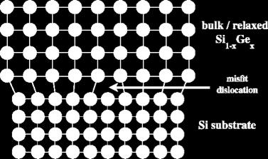
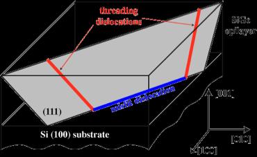
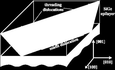
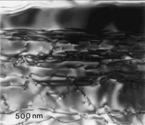
43 43 Relaxation of strain
44 Semiconductor heterostructures Ideal: Heterostructures are formed by semiconductors with the same crystal structure and the same lattice constant: An example is Al Ga As on GaAs Often: Mismatched structures result in misfit dislocations defects which act as recombination centers. An example is GaN on sapphire Diagrams of energy gap-versus-lattice-constant for of different semiconductors 44
45 45


46 Kromer s Central Design Principle of hetero structure Devices 46 Proc IEEE 1982 review paper
47 Double Heterojunction Laser
48 Shockley s 1948 Patent on Hetero transistor 48

49 Abstract of 1982 Kromer s classic HBT review paper 49
Band diagrams of heterostructures
 Herbert Kroemer (1928) 17 Band diagrams of heterostructures 17.1 Band diagram lineups In a semiconductor heterostructure, two different semiconductors are brought into physical contact. In practice, different
Spring Semester 2012 Final Exam
 Spring Semester 2012 Final Exam Note: Show your work, underline results, and always show units. Official exam time: 2.0 hours; an extension of at least 1.0 hour will be granted to anyone. Materials parameters
Session 6: Solid State Physics. Diode
 Session 6: Solid State Physics Diode 1 Outline A B C D E F G H I J 2 Definitions / Assumptions Homojunction: the junction is between two regions of the same material Heterojunction: the junction is between
The discussion about p-n junctions in the semiconductor device is fundamental both
 CHAPTER II MATERIALS JUNCTIONS 2.1 p-n Junctions 2.1.1 Homojunction The discussion about p-n junctions in the semiconductor device is fundamental both in modern electronic applications and in understanding
ECE 440 Lecture 28 : P-N Junction II Class Outline:
 ECE 440 Lecture 28 : P-N Junction II Class Outline: Contact Potential Equilibrium Fermi Levels Things you should know when you leave Key Questions What is the contact potential? Where does the transition
Current mechanisms Exam January 27, 2012
 Current mechanisms Exam January 27, 2012 There are four mechanisms that typically cause currents to flow: thermionic emission, diffusion, drift, and tunneling. Explain briefly which kind of current mechanisms
V BI. H. Föll: kiel.de/matwis/amat/semi_en/kap_2/backbone/r2_2_4.html. different electrochemical potentials (i.e.
 Consider the the band diagram for a homojunction, formed when two bits of the same type of semicondutor (e.g. Si) are doped p and ntype and then brought into contact. Electrons in the two bits have different
Semiconductor Junctions
 8 Semiconductor Junctions Almost all solar cells contain junctions between different materials of different doping. Since these junctions are crucial to the operation of the solar cell, we will discuss
PHYSICAL ELECTRONICS(ECE3540) CHAPTER 9 METAL SEMICONDUCTOR AND SEMICONDUCTOR HETERO-JUNCTIONS
 CHAPTER 9 METAL SEMICONDUCTOR AND SEMICONDUCTOR HETERO-JUNCTIONS") PHYSICAL ELECTRONICS(ECE3540) CHAPTER 9 METAL SEMICONDUCTOR AND SEMICONDUCTOR HETERO-JUNCTIONS Tennessee Technological University Monday, November 11, 013 1 Introduction Chapter 4: we considered the semiconductor
PHYSICAL ELECTRONICS(ECE3540) CHAPTER 9 METAL SEMICONDUCTOR AND SEMICONDUCTOR HETERO-JUNCTIONS Tennessee Technological University Monday, November 11, 013 1 Introduction Chapter 4: we considered the semiconductor
ECE 440 Lecture 20 : PN Junction Electrostatics II Class Outline:
 ECE 440 Lecture 20 : PN Junction Electrostatics II Class Outline: Depletion Approximation Step Junction Things you should know when you leave Key Questions What is the space charge region? What are the
The pn junction. [Fonstad, Ghione]
![The pn junction. [Fonstad, Ghione]](/thumbs/93/112370833.jpg "The pn junction. [Fonstad, Ghione]") The pn junction [Fonstad, Ghione] Band diagram On the vertical axis: potential energy of the electrons On the horizontal axis: now there is nothing: later we ll put the position qf s : work function (F
The pn junction [Fonstad, Ghione] Band diagram On the vertical axis: potential energy of the electrons On the horizontal axis: now there is nothing: later we ll put the position qf s : work function (F
MSE 310/ECE 340: Electrical Properties of Materials Fall 2014 Department of Materials Science and Engineering Boise State University
 MSE 310/ECE 340: Electrical Properties of Materials Fall 2014 Department of Materials Science and Engineering Boise State University Practice Final Exam 1 Read the questions carefully Label all figures
ECE 340 Lecture 21 : P-N Junction II Class Outline:
 ECE 340 Lecture 21 : P-N Junction II Class Outline: Contact Potential Equilibrium Fermi Levels Things you should know when you leave Key Questions What is the contact potential? Where does the transition
Semiconductor Physics and Devices
 The pn Junction 1) Charge carriers crossing the junction. 3) Barrier potential Semiconductor Physics and Devices Chapter 8. The pn Junction Diode 2) Formation of positive and negative ions. 4) Formation
Surfaces, Interfaces, and Layered Devices
 Surfaces, Interfaces, and Layered Devices Building blocks for nanodevices! W. Pauli: God made solids, but surfaces were the work of Devil. Surfaces and Interfaces 1 Interface between a crystal and vacuum
Introduction on the Semiconductor Heterostructures
 Introduction on the Semiconductor Heterostructures Yong Song Department of Physics University of Cincinnati Cincinnati, Ohio 45221 March 07,2002 Abstract:The heterostructure physics becomes more and more
Consider a uniformly doped PN junction, in which one region of the semiconductor is uniformly doped with acceptor atoms and the adjacent region is
 CHAPTER 7 The PN Junction Consider a uniformly doped PN junction, in which one region of the semiconductor is uniformly doped with acceptor atoms and the adjacent region is uniformly doped with donor atoms.
PHYSICAL ELECTRONICS(ECE3540) CHAPTER 9 METAL SEMICONDUCTOR AND SEMICONDUCTOR HETERO-JUNCTIONS
 CHAPTER 9 METAL SEMICONDUCTOR AND SEMICONDUCTOR HETERO-JUNCTIONS") PHYSICAL ELECTRONICS(ECE3540) CHAPTER 9 METAL SEMICONDUCTOR AND SEMICONDUCTOR HETERO-JUNCTIONS Tennessee Technological University Wednesday, October 30, 013 1 Introduction Chapter 4: we considered the
PHYSICAL ELECTRONICS(ECE3540) CHAPTER 9 METAL SEMICONDUCTOR AND SEMICONDUCTOR HETERO-JUNCTIONS Tennessee Technological University Wednesday, October 30, 013 1 Introduction Chapter 4: we considered the
Semiconductor Physics fall 2012 problems
 Semiconductor Physics fall 2012 problems 1. An n-type sample of silicon has a uniform density N D = 10 16 atoms cm -3 of arsenic, and a p-type silicon sample has N A = 10 15 atoms cm -3 of boron. For each
1 Name: Student number: DEPARTMENT OF PHYSICS AND PHYSICAL OCEANOGRAPHY MEMORIAL UNIVERSITY OF NEWFOUNDLAND. Fall :00-11:00
 1 Name: DEPARTMENT OF PHYSICS AND PHYSICAL OCEANOGRAPHY MEMORIAL UNIVERSITY OF NEWFOUNDLAND Final Exam Physics 3000 December 11, 2012 Fall 2012 9:00-11:00 INSTRUCTIONS: 1. Answer all seven (7) questions.
3. Two-dimensional systems
 3. Two-dimensional systems Image from IBM-Almaden 1 Introduction Type I: natural layered structures, e.g., graphite (with C nanostructures) Type II: artificial structures, heterojunctions Great technological
Chapter 7. The pn Junction
 Chapter 7 The pn Junction Chapter 7 PN Junction PN junction can be fabricated by implanting or diffusing donors into a P-type substrate such that a layer of semiconductor is converted into N type. Converting
Schottky Diodes (M-S Contacts)
") Schottky Diodes (M-S Contacts) Three MITs of the Day Band diagrams for ohmic and rectifying Schottky contacts Similarity to and difference from bipolar junctions on electrostatic and IV characteristics.
Schottky Diodes (M-S Contacts) Three MITs of the Day Band diagrams for ohmic and rectifying Schottky contacts Similarity to and difference from bipolar junctions on electrostatic and IV characteristics.
Semiconductor Physics Problems 2015
 Semiconductor Physics Problems 2015 Page and figure numbers refer to Semiconductor Devices Physics and Technology, 3rd edition, by SM Sze and M-K Lee 1. The purest semiconductor crystals it is possible
Introduction on the Semiconductor Heterostructures
 Introduction on the Semiconductor Heterostructures Yong Song Department of Physics University of Cincinnati Cincinnati, OH, 45221 March 7,2002 Abstract: The heterostructure physics becomes more and more
Fundamentals of Semiconductor Physics
 Fall 2007 Fundamentals of Semiconductor Physics 万 歆 Zhejiang Institute of Modern Physics xinwan@zimp.zju.edu.cn http://zimp.zju.edu.cn/~xinwan/ Transistor technology evokes new physics The objective of
ECE-305: Spring 2018 Exam 2 Review
 ECE-305: Spring 018 Exam Review Pierret, Semiconductor Device Fundamentals (SDF) Chapter 3 (pp. 75-138) Chapter 5 (pp. 195-6) Professor Peter Bermel Electrical and Computer Engineering Purdue University,
ECE236A Semiconductor Heterostructure Materials Basic Properties of Semiconductor Heterostructures Lectures 2 & 3 Oct. 5, 2017
 ECE236A Semiconductor Heterostructure Materials Basic Properties of Semiconductor Heterostructures Lectures 2 & 3 Oct. 5, 217 Basic definitions. Types of band-alignment. Determination of band-offsets:
Thermionic emission vs. drift-diffusion vs. p-n junction
 6.772/SMA5111 - Compound Semiconductors Lecture 4 - Carrier flow in heterojunctions - Outline A look at current models for m-s junctions (old business) Thermionic emission vs. drift-diffusion vs. p-n junction
Laser Diodes. Revised: 3/14/14 14: , Henry Zmuda Set 6a Laser Diodes 1
 Laser Diodes Revised: 3/14/14 14:03 2014, Henry Zmuda Set 6a Laser Diodes 1 Semiconductor Lasers The simplest laser of all. 2014, Henry Zmuda Set 6a Laser Diodes 2 Semiconductor Lasers 1. Homojunction
CHAPTER 4: P-N P N JUNCTION Part 2. M.N.A. Halif & S.N. Sabki
 CHAPTER 4: P-N P N JUNCTION Part 2 Part 2 Charge Storage & Transient Behavior Junction Breakdown Heterojunction CHARGE STORAGE & TRANSIENT BEHAVIOR Once injected across the junction, the minority carriers
Semiconductor Devices and Circuits Fall Midterm Exam. Instructor: Dr. Dietmar Knipp, Professor of Electrical Engineering. Name: Mat. -Nr.
 Semiconductor Devices and Circuits Fall 2003 Midterm Exam Instructor: Dr. Dietmar Knipp, Professor of Electrical Engineering Name: Mat. -Nr.: Guidelines: Duration of the Midterm: 1 hour The exam is a closed
R. Ludwig and G. Bogdanov RF Circuit Design: Theory and Applications 2 nd edition. Figures for Chapter 6
 R. Ludwig and G. Bogdanov RF Circuit Design: Theory and Applications 2 nd edition Figures for Chapter 6 Free electron Conduction band Hole W g W C Forbidden Band or Bandgap W V Electron energy Hole Valence
COMPARATIVE ANALYSIS OF BIPOLAR JUNCTION TRANSISTORS AND HETEROJUNCTION BIPOLAR TRANSISTORS USING MATLAB
 Journal of Science and Arts Year 18, No. 1(42), pp. 283-296, 2018 ORIGINAL PAPER COMPARATIVE ANALYSIS OF BIPOLAR JUNCTION TRANSISTORS AND HETEROJUNCTION BIPOLAR TRANSISTORS USING MATLAB GABRIEL PREDUSCA
CME 300 Properties of Materials. ANSWERS: Homework 9 November 26, As atoms approach each other in the solid state the quantized energy states:
 CME 300 Properties of Materials ANSWERS: Homework 9 November 26, 2011 As atoms approach each other in the solid state the quantized energy states: are split. This splitting is associated with the wave
3.1 Introduction to Semiconductors. Y. Baghzouz ECE Department UNLV
 3.1 Introduction to Semiconductors Y. Baghzouz ECE Department UNLV Introduction In this lecture, we will cover the basic aspects of semiconductor materials, and the physical mechanisms which are at the
ρ ρ LED access resistances d A W d s n s p p p W the output window size p-layer d p series access resistance d n n-layer series access resistance
 LED access resistances W the output window size p-layer series access resistance d p n-layer series access resistance d n The n-layer series access resistance R = ρ s n where the resistivity of the n-layer
UNIVERSITY OF CALIFORNIA College of Engineering Department of Electrical Engineering and Computer Sciences. EECS 130 Professor Ali Javey Fall 2006
 UNIVERSITY OF CALIFORNIA College of Engineering Department of Electrical Engineering and Computer Sciences EECS 130 Professor Ali Javey Fall 2006 Midterm 2 Name: SID: Closed book. Two sheets of notes are
Electron Energy, E E = 0. Free electron. 3s Band 2p Band Overlapping energy bands. 3p 3s 2p 2s. 2s Band. Electrons. 1s ATOM SOLID.
 Electron Energy, E Free electron Vacuum level 3p 3s 2p 2s 2s Band 3s Band 2p Band Overlapping energy bands Electrons E = 0 1s ATOM 1s SOLID In a metal the various energy bands overlap to give a single
ECE 340 Lecture 27 : Junction Capacitance Class Outline:
 ECE 340 Lecture 27 : Junction Capacitance Class Outline: Breakdown Review Junction Capacitance Things you should know when you leave M.J. Gilbert ECE 340 Lecture 27 10/24/11 Key Questions What types of
Semiconductor device structures are traditionally divided into homojunction devices
 0. Introduction: Semiconductor device structures are traditionally divided into homojunction devices (devices consisting of only one type of semiconductor material) and heterojunction devices (consisting
Final Examination EE 130 December 16, 1997 Time allotted: 180 minutes
 Final Examination EE 130 December 16, 1997 Time allotted: 180 minutes Problem 1: Semiconductor Fundamentals [30 points] A uniformly doped silicon sample of length 100µm and cross-sectional area 100µm 2
Conductivity and Semi-Conductors
 Conductivity and Semi-Conductors J = current density = I/A E = Electric field intensity = V/l where l is the distance between two points Metals: Semiconductors: Many Polymers and Glasses 1 Electrical Conduction
KATIHAL FİZİĞİ MNT-510
 KATIHAL FİZİĞİ MNT-510 YARIİLETKENLER Kaynaklar: Katıhal Fiziği, Prof. Dr. Mustafa Dikici, Seçkin Yayıncılık Katıhal Fiziği, Şakir Aydoğan, Nobel Yayıncılık, Physics for Computer Science Students: With
SEMICONDUCTOR HETEROJUNCTIONS
 SEMICONDUCTOR HETEROJUNCTIONS February 14, 2012 The University of Toledo, Department of Physics and Astronomy SSARE, PVIC Principles and Varieties of Solar Energy (PHYS 4400) and Fundamentals of Solar
EE 3329 Electronic Devices Syllabus ( Extended Play )
") EE 3329 - Electronic Devices Syllabus EE 3329 Electronic Devices Syllabus ( Extended Play ) The University of Texas at El Paso The following concepts can be part of the syllabus for the Electronic Devices
EE 3329 - Electronic Devices Syllabus EE 3329 Electronic Devices Syllabus ( Extended Play ) The University of Texas at El Paso The following concepts can be part of the syllabus for the Electronic Devices
Review Energy Bands Carrier Density & Mobility Carrier Transport Generation and Recombination
 Review Energy Bands Carrier Density & Mobility Carrier Transport Generation and Recombination The Metal-Semiconductor Junction: Review Energy band diagram of the metal and the semiconductor before (a)
Typical example of the FET: MEtal Semiconductor FET (MESFET)
") Typical example of the FET: MEtal Semiconductor FET (MESFET) Conducting channel (RED) is made of highly doped material. The electron concentration in the channel n = the donor impurity concentration N
Typical example of the FET: MEtal Semiconductor FET (MESFET) Conducting channel (RED) is made of highly doped material. The electron concentration in the channel n = the donor impurity concentration N
LEC E T C U T R U E R E 17 -Photodetectors
 LECTURE 17 -Photodetectors Topics to be covered Photodetectors PIN photodiode Avalanche Photodiode Photodetectors Principle of the p-n junction Photodiode A generic photodiode. Photodetectors Principle
Surfaces, Interfaces, and Layered Devices
 Surfaces, Interfaces, and Layered Devices Building blocks for nanodevices! W. Pauli: God made solids, but surfaces were the work of Devil. Surfaces and Interfaces 1 Role of surface effects in mesoscopic
CLASS 12th. Semiconductors
 CLASS 12th Semiconductors 01. Distinction Between Metals, Insulators and Semi-Conductors Metals are good conductors of electricity, insulators do not conduct electricity, while the semiconductors have
1. Binary III-V compounds 2 p From which atoms are the 16 binary III-V compounds formed?...column III B, Al, Ga and In...column V N, P, As and Sb...
 PROBLEMS part B, Semiconductor Materials. 2006 1. Binary III-V compounds 2 p From which atoms are the 16 binary III-V compounds formed?...column III B, Al, Ga and In...column V N, P, As and Sb... 2. Semiconductors
Electronic Circuits for Mechatronics ELCT 609 Lecture 2: PN Junctions (1)
") Electronic Circuits for Mechatronics ELCT 609 Lecture 2: PN Junctions (1) Assistant Professor Office: C3.315 E-mail: eman.azab@guc.edu.eg 1 Electronic (Semiconductor) Devices P-N Junctions (Diodes): Physical
Electronic Circuits for Mechatronics ELCT 609 Lecture 2: PN Junctions (1) Assistant Professor Office: C3.315 E-mail: eman.azab@guc.edu.eg 1 Electronic (Semiconductor) Devices P-N Junctions (Diodes): Physical
3 Minority carrier profiles (the hyperbolic functions) Consider a
 Consider a") Microelectronic Devices and Circuits October 9, 013 - Homework #3 Due Nov 9, 013 1 Te pn junction Consider an abrupt Si pn + junction tat as 10 15 acceptors cm -3 on te p-side and 10 19 donors on te n-side.
Microelectronic Devices and Circuits October 9, 013 - Homework #3 Due Nov 9, 013 1 Te pn junction Consider an abrupt Si pn + junction tat as 10 15 acceptors cm -3 on te p-side and 10 19 donors on te n-side.
Classification of Solids
 Classification of Solids Classification by conductivity, which is related to the band structure: (Filled bands are shown dark; D(E) = Density of states) Class Electron Density Density of States D(E) Examples
n N D n p = n i p N A
 Summary of electron and hole concentration in semiconductors Intrinsic semiconductor: E G n kt i = pi = N e 2 0 Donor-doped semiconductor: n N D where N D is the concentration of donor impurity Acceptor-doped
pn JUNCTION THE SHOCKLEY MODEL
 The pn Junction: The Shockley Model ( S. O. Kasap, 1990-001) 1 pn JUNCTION THE SHOCKLEY MODEL Safa Kasap Department of Electrical Engineering University of Saskatchewan Canada Although the hole and its
Chapter 1 Overview of Semiconductor Materials and Physics
 Chapter 1 Overview of Semiconductor Materials and Physics Professor Paul K. Chu Conductivity / Resistivity of Insulators, Semiconductors, and Conductors Semiconductor Elements Period II III IV V VI 2 B
Electronics The basics of semiconductor physics
 Electronics The basics of semiconductor physics Prof. Márta Rencz, Gergely Nagy BME DED September 16, 2013 The basic properties of semiconductors Semiconductors conductance is between that of conductors
16EC401 BASIC ELECTRONIC DEVICES UNIT I PN JUNCTION DIODE. Energy Band Diagram of Conductor, Insulator and Semiconductor:
 16EC401 BASIC ELECTRONIC DEVICES UNIT I PN JUNCTION DIODE Energy bands in Intrinsic and Extrinsic silicon: Energy Band Diagram of Conductor, Insulator and Semiconductor: 1 2 Carrier transport: Any motion
Metal Semiconductor Contacts
 Metal Semiconductor Contacts The investigation of rectification in metal-semiconductor contacts was first described by Braun [33-35], who discovered in 1874 the asymmetric nature of electrical conduction
Direct and Indirect Semiconductor
 Direct and Indirect Semiconductor Allowed values of energy can be plotted vs. the propagation constant, k. Since the periodicity of most lattices is different in various direction, the E-k diagram must
Effective masses in semiconductors
 Effective masses in semiconductors The effective mass is defined as: In a solid, the electron (hole) effective mass represents how electrons move in an applied field. The effective mass reflects the inverse
Engineering 2000 Chapter 8 Semiconductors. ENG2000: R.I. Hornsey Semi: 1
 Engineering 2000 Chapter 8 Semiconductors ENG2000: R.I. Hornsey Semi: 1 Overview We need to know the electrical properties of Si To do this, we must also draw on some of the physical properties and we
ET3034TUx Utilization of band gap energy
 ET3034TUx - 3.3.1 - Utilization of band gap energy In the last two weeks we have discussed the working principle of a solar cell and the external parameters that define the performance of a solar cell.
6.012 Electronic Devices and Circuits
 Page 1 of 1 YOUR NAME Department of Electrical Engineering and Computer Science Massachusetts Institute of Technology 6.12 Electronic Devices and Circuits Exam No. 1 Wednesday, October 7, 29 7:3 to 9:3
Lecture 9: Metal-semiconductor junctions
 Lecture 9: Metal-semiconductor junctions Contents 1 Introduction 1 2 Metal-metal junction 1 2.1 Thermocouples.......................... 2 3 Schottky junctions 4 3.1 Forward bias............................
Semiconductor Physics fall 2012 problems
 Semiconductor Physics fall 2012 problems 1. An n-type sample of silicon has a uniform density N D = 10 16 atoms cm -3 of arsenic, and a p-type silicon sample has N A = 10 15 atoms cm -3 of boron. For each
Lecture 3: Heterostructures, Quasielectric Fields, and Quantum Structures
 Lecture 3: Heterostructures, Quasielectric Fields, and Quantum Structures MSE 6001, Semiconductor Materials Lectures Fall 2006 3 Semiconductor Heterostructures A semiconductor crystal made out of more
Lecture 8. Equations of State, Equilibrium and Einstein Relationships and Generation/Recombination
 Lecture 8 Equations of State, Equilibrium and Einstein Relationships and Generation/Recombination Reading: (Cont d) Notes and Anderson 2 sections 3.4-3.11 Energy Equilibrium Concept Consider a non-uniformly
Physics of Semiconductors
 Physics of Semiconductors 9 th 2016.6.13 Shingo Katsumoto Department of Physics and Institute for Solid State Physics University of Tokyo Site for uploading answer sheet Outline today Answer to the question
Session 5: Solid State Physics. Charge Mobility Drift Diffusion Recombination-Generation
 Session 5: Solid State Physics Charge Mobility Drift Diffusion Recombination-Generation 1 Outline A B C D E F G H I J 2 Mobile Charge Carriers in Semiconductors Three primary types of carrier action occur
ECE-305: Spring 2018 Final Exam Review
 C-305: Spring 2018 Final xam Review Pierret, Semiconductor Device Fundamentals (SDF) Chapters 10 and 11 (pp. 371-385, 389-403) Professor Peter Bermel lectrical and Computer ngineering Purdue University,
Chapter 5. Semiconductor Laser
 Chapter 5 Semiconductor Laser 5.0 Introduction Laser is an acronym for light amplification by stimulated emission of radiation. Albert Einstein in 1917 showed that the process of stimulated emission must
ECE 305 Exam 2: Spring 2017 March 10, 2017 Muhammad Alam Purdue University
 NAME: PUID: : ECE 305 Exam 2: Spring 2017 March 10, 2017 Muhammad Alam Purdue University This is a closed book exam You may use a calculator and the formula sheet Following the ECE policy, the calculator
Introduction to Optoelectronic Device Simulation by Joachim Piprek
 NUSOD 5 Tutorial MA Introduction to Optoelectronic Device Simulation by Joachim Piprek Outline:. Introduction: VCSEL Example. Electron Energy Bands 3. Drift-Diffusion Model 4. Thermal Model 5. Gain/Absorption
Lecture 15 - The pn Junction Diode (I) I-V Characteristics. November 1, 2005
 I-V Characteristics. November 1, 2005") 6.012 - Microelectronic Devices and Circuits - Fall 2005 Lecture 15-1 Lecture 15 - The pn Junction Diode (I) I-V Characteristics November 1, 2005 Contents: 1. pn junction under bias 2. I-V characteristics
6.012 - Microelectronic Devices and Circuits - Fall 2005 Lecture 15-1 Lecture 15 - The pn Junction Diode (I) I-V Characteristics November 1, 2005 Contents: 1. pn junction under bias 2. I-V characteristics
Photodetector. Prof. Woo-Young Choi. Silicon Photonics (2012/2) Photodetection: Absorption => Current Generation. Currents
 Photodetection: Absorption => Current Generation. Currents") Photodetection: Absorption => Current Generation h Currents Materials for photodetection: E g < h Various methods for generating currents with photo-generated carriers: photoconductors, photodiodes, avalanche
Photodetection: Absorption => Current Generation h Currents Materials for photodetection: E g < h Various methods for generating currents with photo-generated carriers: photoconductors, photodiodes, avalanche
Institute of Solid State Physics. Technische Universität Graz. Exam. Feb 2, 10:00-11:00 P2
 Technische Universität Graz nstitute of Solid State Physics Exam Feb 2, 10:00-11:00 P2 Exam Four questions, two from the online list. Calculator is ok. No notes. Explain some concept: (tunnel contact,
ECE 340 Lecture 35 : Metal- Semiconductor Junctions Class Outline:
 ECE 340 Lecture 35 : - Junctions Class Outline: Ideal - Contacts Rectifying Contacts Ohmic Contacts Things you should know when you leave Key Questions What happens to the bands when we make contact between
Semiconductor Physics. Lecture 3
 Semiconductor Physics Lecture 3 Intrinsic carrier density Intrinsic carrier density Law of mass action Valid also if we add an impurity which either donates extra electrons or holes the number of carriers
Peak Electric Field. Junction breakdown occurs when the peak electric field in the PN junction reaches a critical value. For the N + P junction,
 Peak Electric Field Junction breakdown occurs when the peak electric field in the P junction reaches a critical value. For the + P junction, qa E ( x) ( xp x), s W dep 2 s ( bi Vr ) 2 s potential barrier
Introduction to Sources: Radiative Processes and Population Inversion in Atoms, Molecules, and Semiconductors Atoms and Molecules
 OPTI 500 DEF, Spring 2012, Lecture 2 Introduction to Sources: Radiative Processes and Population Inversion in Atoms, Molecules, and Semiconductors Atoms and Molecules Energy Levels Every atom or molecule
Solid State Physics SEMICONDUCTORS - IV. Lecture 25. A.H. Harker. Physics and Astronomy UCL
 Solid State Physics SEMICONDUCTORS - IV Lecture 25 A.H. Harker Physics and Astronomy UCL 9.9 Carrier diffusion and recombination Suppose we have a p-type semiconductor, i.e. n h >> n e. (1) Create a local
Lecture 12. Semiconductor Detectors - Photodetectors
 Lecture 12 Semiconductor Detectors - Photodetectors Principle of the pn junction photodiode Absorption coefficient and photodiode materials Properties of semiconductor detectors The pin photodiodes Avalanche
FREQUENTLY ASKED QUESTIONS February 21, 2017
 FREQUENTLY ASKED QUESTIONS February 21, 2017 Content Questions How do you place a single arsenic atom with the ratio 1 in 100 million? Sounds difficult to get evenly spread throughout. Yes, techniques
ECE 340 Lecture 39 : MOS Capacitor II
 ECE 340 Lecture 39 : MOS Capacitor II Class Outline: Effects of Real Surfaces Threshold Voltage MOS Capacitance-Voltage Analysis Things you should know when you leave Key Questions What are the effects
Avalanche breakdown. Impact ionization causes an avalanche of current. Occurs at low doping
 Avalanche breakdown Impact ionization causes an avalanche of current Occurs at low doping Zener tunneling Electrons tunnel from valence band to conduction band Occurs at high doping Tunneling wave decays
Unit IV Semiconductors Engineering Physics
 Introduction A semiconductor is a material that has a resistivity lies between that of a conductor and an insulator. The conductivity of a semiconductor material can be varied under an external electrical
The Law of the Junction Revisited. Mark Lundstrom Network for Computational Nanotechnology and Purdue University ( ). (1)
. (1)") The Law of the Junction Revisited Mark Lundstrom Network for Computational Nanotechnology and Purdue University Consider a one-sided, short base diode like that shown in Fig.. We usually analyze the I-V
The Law of the Junction Revisited Mark Lundstrom Network for Computational Nanotechnology and Purdue University Consider a one-sided, short base diode like that shown in Fig.. We usually analyze the I-V
Semiconductor Physics. Lecture 6
 Semiconductor Physics Lecture 6 Recap pn junction and the depletion region Driven by the need to have no gradient in the fermi level free carriers migrate across the pn junction leaving a region with few
ESE 372 / Spring 2013 / Lecture 5 Metal Oxide Semiconductor Field Effect Transistor
 Metal Oxide Semiconductor Field Effect Transistor V G V G 1 Metal Oxide Semiconductor Field Effect Transistor We will need to understand how this current flows through Si What is electric current? 2 Back
Quiz #1 Practice Problem Set
 Name: Student Number: ELEC 3908 Physical Electronics Quiz #1 Practice Problem Set? Minutes January 22, 2016 - No aids except a non-programmable calculator - All questions must be answered - All questions
Schottky diodes. JFETs - MESFETs - MODFETs
 Technische Universität Graz Institute of Solid State Physics Schottky diodes JFETs - MESFETs - MODFETs Quasi Fermi level When the charge carriers are not in equilibrium the Fermi energy can be different
Semiconductor Physics and Devices Chapter 3.
 Introduction to the Quantum Theory of Solids We applied quantum mechanics and Schrödinger s equation to determine the behavior of electrons in a potential. Important findings Semiconductor Physics and
ECE 305 Fall Final Exam (Exam 5) Wednesday, December 13, 2017
 Wednesday, December 13, 2017") NAME: PUID: ECE 305 Fall 017 Final Exam (Exam 5) Wednesday, December 13, 017 This is a closed book exam. You may use a calculator and the formula sheet at the end of this exam. Following the ECE policy,
NAME: PUID: ECE 305 Fall 017 Final Exam (Exam 5) Wednesday, December 13, 017 This is a closed book exam. You may use a calculator and the formula sheet at the end of this exam. Following the ECE policy,
PHYS485 Materials Physics
 5/11/017 PHYS485 Materials Physics Dr. Gregory W. Clar Manchester University LET S GO ON A (TEK)ADVENTURE! WHAT? TRIP TO A MAKER S SPACE IN FORT WAYNE WHEN? THURSDAY, MAY 11 TH @ 5PM WHERE? TEKVENTURE
Figure 3.1 (p. 141) Figure 3.2 (p. 142)
 Figure 3.2 (p. 142)") Figure 3.1 (p. 141) Allowed electronic-energy-state systems for two isolated materials. States marked with an X are filled; those unmarked are empty. System 1 is a qualitative representation of a metal;
Figure 3.1 (p. 141) Allowed electronic-energy-state systems for two isolated materials. States marked with an X are filled; those unmarked are empty. System 1 is a qualitative representation of a metal;
Semiconductor Optoelectronics Prof. M. R. Shenoy Department of Physics Indian Institute of Technology, Delhi. Lecture - 13 Band gap Engineering
 Semiconductor Optoelectronics Prof. M. R. Shenoy Department of Physics Indian Institute of Technology, Delhi Lecture - 13 Band gap Engineering (Refer Slide Time: 00:38) Let us continue with the lectures,
UNIVERSITY OF CALIFORNIA College of Engineering Department of Electrical Engineering and Computer Sciences. EECS 130 Professor Ali Javey Fall 2006
 UNIVERSITY OF CALIFORNIA College of Engineering Department of Electrical Engineering and Computer Sciences EECS 130 Professor Ali Javey Fall 2006 Midterm I Name: Closed book. One sheet of notes is allowed.