Physicists in the Semiconductor Industry
|
|
|
- George Jeremy Holland
- 5 years ago
- Views:
Transcription

1 Physicists in the Semiconductor Industry P.M. Mooney IBM Research Division, T.J. Watson Research Center Yorktown Heights, NY APS March Meeting March 24, 2004 Thomas J. Watson Research Center 1
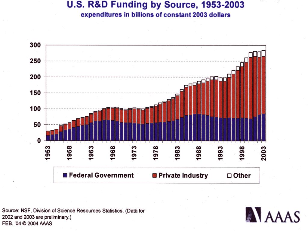
2 Outline - Introduction - R&D funding in the US - evolution of semiconductor technology - Physics research in the semiconductor industry - current materials issues in Si CMOS technology - materials characterization issues - Physicists in the semiconductor industry - requirements - career paths 2
3 3
4 4
5 Information Technology Enabled by Semiconductor Technology Highlights in the evolution of semiconductor technology: electron discovered 1898 semiconductor properties understood 1920's and 30's bulk crystal growth methods high quality crystals point contact transistor 1947 Ge junction transistor 1948 Ge photovoltaic device (solar cell) 1954 Si fully transistorized computer operations/sec, 800 transistors integrated circuit invented 1958 Si diode laser 1962 GaAs Si memory chips available bits first microprosessor transistors epitaxial crystal growth methods 1970s layered semiconductor heterostructures - study of quantum effects - quantum effect electronic devices Apple II st assembled PC (not a kit) IBM PC 1981 Cray-2 (supercomputer) logic operations/sec World Wide Web 1990 proposal for standard addresses GPS completed Navstar satellites/atomic clocks Pentium III processor million transistors 5
6 Moore's Law -- in 1965 Gordon Moore predicted that the number of components on the most complex chips would double every year for 10 years Exponential increases in performance for >30 years! Transistor performance increases primarily due to scaling -- reduction in the size of individual devices Key factors in overall performance increase of ICs: 50% -- improvement in lithograpy (determines size of smallest features) 25% -- larger chip size 25% -- innovations in fabrication methods/new materials # components/chip increases faster than cost/chip ==> exponential decrease in cost/function fuels information age! 6
7 Faster Computers Need Faster Transistors source gate drain scaling source gate drain gate dielectric Si Si smaller transistor is faster: electrons move a shorter distance - standard gate dielectric in SiO 2 - tunneling current increases as layer becomes thinner - leads to high power consumption in IC - find a new gate dielectric material with larger dielectric constant - the physical thickness of the layer can be larger ==> reduced tunneling current in scaled devices 7
8 Faster Computers Need Faster Transistors source gate drain scaling source gate drain Si Si smaller transistor is faster: electrons move a shorter distance - dopant atoms are implanted to form source and drain regions - dopant diffusion is hard to control at nm dimensions - lateral diffusion can lead to shorted devices - e.g. transient enhanced diffusion is a problem - need to understand dopant diffusion better - need new characterization methods for dopant distribution 8
9 Faster Computers Need Faster Transistors source gate drain Si find a new material in which charge carriers have higher mobility (v = E, where mobility,, is a function of effective mass, m*) source gate SiGe buffer layer Si drain strained silicon epitaxial SiGe/Si heterostructure 9
10 Materials Requirements for CMOS - desired physical characteristics - e.g., dielectric constant, electron mobility - compatible with fabrication processes - high processing temperatures (up to 1000 o C) - similar thermal expansion coefficient - reliability - integrated circuit should last 10 years - manufacturablity - cost ===> physics is just the beginning!! 10
11 Characterization/Metrology Issues - must be able to characterize what you make! - structural characterization electron microscopy (SEM, TEM) x-ray difraction (lattice parameter/strain) x-ray reflectivity (film thickness and roughness) spectroscopy ellipsometry (film thickness) Raman spectroscopy (strain) - Chemical Characterization secondary ion mass spectrometry Aujer electron spectroscopy Rutherford back scattering - electrical characterization carrier mobility charge density at interfaces resistivity device characteristics - automated measurements needed in manufacturing! - fast data collection - data management - collaborations with equipment companies 11

12 New Characterization Methods: Electron Holography - electron beam is split to obtain phase information as well as amplitude information - obtain electrical potential from phase information - demonstrated use to image dopant distribution in short-gate CMOS devices - quantative measurement of dopant profile in device - learn about dopant diffusion - developed as routine method for failure analysis IBM - Arizona State U. collaboration - Gribelyuk, et al., Phys. Rev. Lett. 89, (2002) - M.R. McCartney, et al. Appl. Phys. Lett. 80, 3213 (2002). 12
 probe size by means of a computer controlled aberration correction system allows imaging of single atoms, clusters of a few atoms, single atomic layers, single column of atoms in a")
13 Improved Scanning Transmission Electron Microscopy - high spatial resolution structural imaging plus electron energy loss spectroscopy for electronic structure - recently achieved sub-angstrom (0.078 nm) probe size by means of a computer controlled aberration correction system allows imaging of single atoms, clusters of a few atoms, single atomic layers, single column of atoms in a semiconductor 90 Partial Dislocation Structure On the left: Model calculation showing a proposed structure for an important defect in the silicon crystal, viewed using a 2 Angstrom (0.2 nanometers) resolution. Atom columns are indicated by the dots. Near neighbor connectivity of the atoms is indicated by the lines. Bright areas indicate strong scattering of the 2 Angstrom electron beam. On the right: The same structure viewed with a 1 Angstrom diameter beam. Details in the four column group (red) will become apparent. P.E. Batson et al., Nature 418, 617 (2002). P.E.Batson, Ultramicroscopy 96, 239 (2003). 13
 0.20 0.15 0.10 0.05 line scan 0.00-0.95-0.90-0.85-0.80-0.")

14 X-Ray Microdiffraction: Image Dislocations in SiGe Layers scanning microtopograph 0.25 Intensity (arb.units) line scan X Position (mm) 200 m x 200 m dark features are >7 nm wide! XTEM shows that features are dislocation pile-ups, not individual dislocations! P.M. Mooney, et al., Appl. Phys. Lett. 79, 2363 (2001). TEM image diameter = 6.7 m 14
 diffraction from strained Si regions - extends 120 m beyond edge of dot (long range effect) - similar effect seen for smaller SiGe/Si")
15 X-Ray Microdiffraction: Measure Strain at Small Features 190 m-diameter polycrystalline Ni dots on a Si(111) substrate Ni K fluorescence intensity of Si 333 peak - diffracted intensity is increased at edge of dot - enhancement due to kinematic (not dynamic) diffraction from strained Si regions - extends 120 m beyond edge of dot (long range effect) - similar effect seen for smaller SiGe/Si features I.C. Noyan, et al., APL 74, 2352 (1999). C.E. Murray, et al., APL 83, 4163 (2003). 15
16 Requirements for PhD Researchers - strong scientific or technical background PhD in physics, chemistry or engineering - creativity/innovation - interest in solving problems research in industry is mission oriented important to apply knowledge to future products - leadership technical leadership project leadership convince others to work on your ideas management of research/development - communications skills speaking and writing - ability to work with people in interdisciplinary teams 16
17 Research Staff Member: Pat Mooney - research in semiconductor defects - electronic states of defects (DLTS) - strain relxation in lattice mismatched structures (XRD) - project leader - various projects related to SiGe/Si materials and devices - active in research community - organizing national and internations conferences - editorial boards of journals - American Physical Society Chair, Division of Materials Physics Councillor, Forum of Industrial and Applied Physics - primary responsibility is doing research 17
18 Research Management: Tom Theis Resarch Staff Member: - research on transport in semiconductors - manager of III-V semiconductor epitaxy group - manager of III-V semiconductor epitaxy and device groups - manager of semiconductor research department - manager of CMOS materials research department Director of Physical Sciences Department (executive) - responsible for Research Division physical sciences research strategy and planning (includes research at Watson, Almaden and Zurich labs) 18
19 Technology Management: Bernie Meyerson Research Staff Member: - research on growth of Si and SiGe films at low temperature - invented UHVCVD - manager of SiGe materials group - demonstrated SiGe heterojunction bipolar transistor - manager of SiGe materials and device groups - iniated development of IBM's analog and mixed signal circuits for telecommunications applications Director of Communications Technology Department included groups in both the Research and the Microelectronics Divisions Vice President and Director of Communications Research and Development Center included departments in both the Research and the Microelectronics Divisions Vice President and Chief Strategist, IBM Technology Group responsible for product development activities in microelectronics many science and engineering researchers move into technology management! 19
20 Services Management: Francoise LeGoues Research Staff Member - materials physics using electron microscopy methods - manager, physical sciences electron microscopy group - technical assistant to Director of Mathematical Sciences Department (research executive responsible for utilities industry) Marketing Division - worked to initiate research activities related to utilities industry - managed IBM customer center (established to show new research products to customers Director, Inovation and Technology, IBM Global Services Division - linkage between research, IBM Global services and Customers - impact of technology on customers - organizational transformation through technical innovation uses technical background for work with IBM customers 20
21 Summary Research in the semiconductor industry - mission oriented -- e.g., faster/lower power ICs - applied physics research - new materials are is essential - new characterization methods are essential Physics PhDs are sought for - innovation/creativity - ability in problem solving - interest in applications of research for products - scientific and technical leadership - research management - technology management - marketing and services management 21
Currently, worldwide major semiconductor alloy epitaxial growth is divided into two material groups.
 ICQNM 2014 Currently, worldwide major semiconductor alloy epitaxial growth is divided into two material groups. Cubic: Diamond structures: group IV semiconductors (Si, Ge, C), Cubic zinc-blende structures:
EE130: Integrated Circuit Devices
 EE130: Integrated Circuit Devices (online at http://webcast.berkeley.edu) Instructor: Prof. Tsu-Jae King (tking@eecs.berkeley.edu) TA s: Marie Eyoum (meyoum@eecs.berkeley.edu) Alvaro Padilla (apadilla@eecs.berkeley.edu)
Three-Dimensional Silicon-Germanium Nanostructures for Light Emitters and On-Chip Optical. Interconnects
 Three-Dimensional Silicon-Germanium Nanostructures for Light Emitters and On-Chip Optical eptember 2011 Interconnects Leonid Tsybeskov Department of Electrical and Computer Engineering New Jersey Institute
Transistor and Integrated Circuits: History
 Course Objective Review and practice fundamental chemical engineering concepts (mass, energy, and momentum transport coupled with heterogeneous and homogeneous reactions and thermodynamics). Apply these
Nanoelectronics. Topics
 Nanoelectronics Topics Moore s Law Inorganic nanoelectronic devices Resonant tunneling Quantum dots Single electron transistors Motivation for molecular electronics The review article Overview of Nanoelectronic
EE 5211 Analog Integrated Circuit Design. Hua Tang Fall 2012
 EE 5211 Analog Integrated Circuit Design Hua Tang Fall 2012 Today s topic: 1. Introduction to Analog IC 2. IC Manufacturing (Chapter 2) Introduction What is Integrated Circuit (IC) vs discrete circuits?
Post Von Neumann Computing
 Post Von Neumann Computing Matthias Kaiserswerth Hasler Stiftung (formerly IBM Research) 1 2014 IBM Corporation Foundation Purpose Support information and communication technologies (ICT) to advance Switzerland
EV Group. Engineered Substrates for future compound semiconductor devices
 EV Group Engineered Substrates for future compound semiconductor devices Engineered Substrates HB-LED: Engineered growth substrates GaN / GaP layer transfer Mobility enhancement solutions: III-Vs to silicon
Quantum and Non-local Transport Models in Crosslight Device Simulators. Copyright 2008 Crosslight Software Inc.
 Quantum and Non-local Transport Models in Crosslight Device Simulators Copyright 2008 Crosslight Software Inc. 1 Introduction Quantization effects Content Self-consistent charge-potential profile. Space
ECE Semiconductor Device and Material Characterization
 ECE 4813 Semiconductor Device and Material Characterization Dr. Alan Doolittle School of Electrical and Computer Engineering Georgia Institute of Technology As with all of these lecture slides, I am indebted
Solid State Device Fundamentals
 Solid State Device Fundamentals ENS 345 Lecture Course by Alexander M. Zaitsev alexander.zaitsev@csi.cuny.edu Tel: 718 982 2812 Office 4N101b 1 Outline - Goals of the course. What is electronic device?
Optical Spectroscopies of Thin Films and Interfaces. Dietrich R. T. Zahn Institut für Physik, Technische Universität Chemnitz, Germany
 Optical Spectroscopies of Thin Films and Interfaces Dietrich R. T. Zahn Institut für Physik, Technische Universität Chemnitz, Germany 1. Introduction 2. Vibrational Spectroscopies (Raman and Infrared)
Current mechanisms Exam January 27, 2012
 Current mechanisms Exam January 27, 2012 There are four mechanisms that typically cause currents to flow: thermionic emission, diffusion, drift, and tunneling. Explain briefly which kind of current mechanisms
Nanotechnology Nanofabrication of Functional Materials. Marin Alexe Max Planck Institute of Microstructure Physics, Halle - Germany
 Nanotechnology Nanofabrication of Functional Materials Marin Alexe Max Planck Institute of Microstructure Physics, Halle - Germany Contents Part I History and background to nanotechnology Nanoworld Nanoelectronics
Nanostructure. Materials Growth Characterization Fabrication. More see Waser, chapter 2
 Nanostructure Materials Growth Characterization Fabrication More see Waser, chapter 2 Materials growth - deposition deposition gas solid Physical Vapor Deposition Chemical Vapor Deposition Physical Vapor
MEMS Metrology. Prof. Tianhong Cui ME 8254
 MEMS Metrology Prof. Tianhong Cui ME 8254 What is metrology? Metrology It is the science of weights and measures Refers primarily to the measurements of length, weight, time, etc. Mensuration- A branch
Electrical Characterization with SPM Application Modules
 Electrical Characterization with SPM Application Modules Metrology, Characterization, Failure Analysis: Data Storage Magnetoresistive (MR) read-write heads Semiconductor Transistors Interconnect Ferroelectric
EE 527 MICROFABRICATION. Lecture 5 Tai-Chang Chen University of Washington
 EE 527 MICROFABRICATION Lecture 5 Tai-Chang Chen University of Washington MICROSCOPY AND VISUALIZATION Electron microscope, transmission electron microscope Resolution: atomic imaging Use: lattice spacing.
Solid Surfaces, Interfaces and Thin Films
 Hans Lüth Solid Surfaces, Interfaces and Thin Films Fifth Edition With 427 Figures.2e Springer Contents 1 Surface and Interface Physics: Its Definition and Importance... 1 Panel I: Ultrahigh Vacuum (UHV)
Analytical Modeling of Threshold Voltage for a. Biaxial Strained-Si-MOSFET
 Contemporary Engineering Sciences, Vol. 4, 2011, no. 6, 249 258 Analytical Modeling of Threshold Voltage for a Biaxial Strained-Si-MOSFET Amit Chaudhry Faculty of University Institute of Engineering and
phys4.20 Page 1 - the ac Josephson effect relates the voltage V across a Junction to the temporal change of the phase difference
 Josephson Effect - the Josephson effect describes tunneling of Cooper pairs through a barrier - a Josephson junction is a contact between two superconductors separated from each other by a thin (< 2 nm)
Classification of Solids
 Classification of Solids Classification by conductivity, which is related to the band structure: (Filled bands are shown dark; D(E) = Density of states) Class Electron Density Density of States D(E) Examples
Stretching the Barriers An analysis of MOSFET Scaling. Presenters (in order) Zeinab Mousavi Stephanie Teich-McGoldrick Aseem Jain Jaspreet Wadhwa
 Zeinab Mousavi Stephanie Teich-McGoldrick Aseem Jain Jaspreet Wadhwa") Stretching the Barriers An analysis of MOSFET Scaling Presenters (in order) Zeinab Mousavi Stephanie Teich-McGoldrick Aseem Jain Jaspreet Wadhwa Why Small? Higher Current Lower Gate Capacitance Higher
Stretching the Barriers An analysis of MOSFET Scaling Presenters (in order) Zeinab Mousavi Stephanie Teich-McGoldrick Aseem Jain Jaspreet Wadhwa Why Small? Higher Current Lower Gate Capacitance Higher
Single ion implantation for nanoelectronics and the application to biological systems. Iwao Ohdomari Waseda University Tokyo, Japan
 Single ion implantation for nanoelectronics and the application to biological systems Iwao Ohdomari Waseda University Tokyo, Japan Contents 1.History of single ion implantation (SII) 2.Novel applications
Chapter 3 Basics Semiconductor Devices and Processing
 Chapter 3 Basics Semiconductor Devices and Processing Hong Xiao, Ph. D. www2.austin.cc.tx.us/hongxiao/book.htm Hong Xiao, Ph. D. www2.austin.cc.tx.us/hongxiao/book.htm 1 Objectives Identify at least two
Novel materials and nanostructures for advanced optoelectronics
 Novel materials and nanostructures for advanced optoelectronics Q. Zhuang, P. Carrington, M. Hayne, A Krier Physics Department, Lancaster University, UK u Brief introduction to Outline Lancaster University
Infrared Reflectivity Spectroscopy of Optical Phonons in Short-period AlGaN/GaN Superlattices
 Infrared Reflectivity Spectroscopy of Optical Phonons in Short-period AlGaN/GaN Superlattices J. B. Herzog, A. M. Mintairov, K. Sun, Y. Cao, D. Jena, J. L. Merz. University of Notre Dame, Dept. of Electrical
From nanophysics research labs to cell phones. Dr. András Halbritter Department of Physics associate professor
 From nanophysics research labs to cell phones Dr. András Halbritter Department of Physics associate professor Curriculum Vitae Birth: 1976. High-school graduation: 1994. Master degree: 1999. PhD: 2003.
Nanoparticle Devices. S. A. Campbell, ECE C. B. Carter, CEMS H. Jacobs, ECE J. Kakalios, Phys. U. Kortshagen, ME. Institute of Technology
 Nanoparticle Devices S. A. Campbell, ECE C. B. Carter, CEMS H. Jacobs, ECE J. Kakalios, Phys. U. Kortshagen, ME Applications of nanoparticles Flash Memory Tiwari et al., Appl. Phys. Lett. 68, 1377, 1996.
High-Precision Evaluation of Ultra-Shallow Impurity Profiles by Secondary Ion Mass Spectrometry
 High-Precision Evaluation of Ultra-Shallow Impurity Profiles by Secondary Ion Mass Spectrometry Yoko Tada Kunihiro Suzuki Yuji Kataoka (Manuscript received December 28, 2009) As complementary metal oxide
ECE Semiconductor Device and Material Characterization
 ECE 4813 Semiconductor Device and Material Characterization Dr. Alan Doolittle School of Electrical and Computer Engineering Georgia Institute of Technology As with all of these lecture slides, I am indebted
Lecture 20: Semiconductor Structures Kittel Ch 17, p , extra material in the class notes
 Lecture 20: Semiconductor Structures Kittel Ch 17, p 494-503, 507-511 + extra material in the class notes MOS Structure Layer Structure metal Oxide insulator Semiconductor Semiconductor Large-gap Semiconductor
IBM T.J. Watson Research Center
 IBM T.J. Watson Research Center 2D material based layer transfer Jeehwan Kim Prof. of Mechanical Engineering Prof. of Materials science and Engineering Jeehwan Kim Research Group http://jeehwanlab.mit.edu
Lecture 3: Heterostructures, Quasielectric Fields, and Quantum Structures
 Lecture 3: Heterostructures, Quasielectric Fields, and Quantum Structures MSE 6001, Semiconductor Materials Lectures Fall 2006 3 Semiconductor Heterostructures A semiconductor crystal made out of more
Self-study problems and questions Processing and Device Technology, FFF110/FYSD13
 Self-study problems and questions Processing and Device Technology, FFF110/FYSD13 Version 2016_01 In addition to the problems discussed at the seminars and at the lectures, you can use this set of problems
(a) (b) Supplementary Figure 1. (a) (b) (a) Supplementary Figure 2. (a) (b) (c) (d) (e)
 (b) Supplementary Figure 1. (a) (b) (a) Supplementary Figure 2. (a) (b) (c) (d) (e)") (a) (b) Supplementary Figure 1. (a) An AFM image of the device after the formation of the contact electrodes and the top gate dielectric Al 2 O 3. (b) A line scan performed along the white dashed line
(a) (b) Supplementary Figure 1. (a) An AFM image of the device after the formation of the contact electrodes and the top gate dielectric Al 2 O 3. (b) A line scan performed along the white dashed line
MS482 Materials Characterization ( 재료분석 ) Lecture Note 2: UPS
 Lecture Note 2: UPS") 2016 Fall Semester MS482 Materials Characterization ( 재료분석 ) Lecture Note 2: UPS Byungha Shin Dept. of MSE, KAIST 1 Course Information Syllabus 1. Overview of various characterization techniques (1 lecture)
2016 Fall Semester MS482 Materials Characterization ( 재료분석 ) Lecture Note 2: UPS Byungha Shin Dept. of MSE, KAIST 1 Course Information Syllabus 1. Overview of various characterization techniques (1 lecture)
Chapter 10. Nanometrology. Oxford University Press All rights reserved.
 Chapter 10 Nanometrology Oxford University Press 2013. All rights reserved. 1 Introduction Nanometrology is the science of measurement at the nanoscale level. Figure illustrates where nanoscale stands
Prospects for Ge MOSFETs
 Prospects for Ge MOSFETs Sematech Workshop December 4, 2005 Dimitri A. Antoniadis Microsystems Technology Laboratories MIT Sematech Workshop 2005 1 Channel Transport - I D I D =WQ i (x 0 )v xo v xo : carrier
Creating atomic order in semiconductors quantum dots
 Creating atomic order in semiconductors quantum dots Peter Moeck Department of Physics (MC 273), 845 W. Taylor Street, Chicago, Illinois 60607-7059 collaborations with Teya Topuria, Yuanyuan Lei, Nigel
Sheng S. Li. Semiconductor Physical Electronics. Second Edition. With 230 Figures. 4) Springer
 Springer") Sheng S. Li Semiconductor Physical Electronics Second Edition With 230 Figures 4) Springer Contents Preface 1. Classification of Solids and Crystal Structure 1 1.1 Introduction 1 1.2 The Bravais Lattice
Sheng S. Li Semiconductor Physical Electronics Second Edition With 230 Figures 4) Springer Contents Preface 1. Classification of Solids and Crystal Structure 1 1.1 Introduction 1 1.2 The Bravais Lattice
Putting quantum dot lasers to practical use
 Enviroment Life Nanotechnology Information Science Reconstruction Others Science and and Technology andfrom Energy Communications andthe Materials for Great Society EastTechnology Japan Earthquake (FY2017
Metrology is not a cost factor, but a profit center
 Edition February 2018 Semiconductor technology & processing Metrology is not a cost factor, but a profit center In recent years, remarkable progress has been made in the field of metrology, which is crucial
Nanoelectronics 09. Atsufumi Hirohata Department of Electronics. Quick Review over the Last Lecture
 Nanoelectronics 09 Atsufumi Hirohata Department of Electronics 13:00 Monday, 12/February/2018 (P/T 006) Quick Review over the Last Lecture ( Field effect transistor (FET) ): ( Drain ) current increases
How a single defect can affect silicon nano-devices. Ted Thorbeck
 How a single defect can affect silicon nano-devices Ted Thorbeck tedt@nist.gov The Big Idea As MOS-FETs continue to shrink, single atomic scale defects are beginning to affect device performance Gate Source
Monolayer Semiconductors
 Monolayer Semiconductors Gilbert Arias California State University San Bernardino University of Washington INT REU, 2013 Advisor: Xiaodong Xu (Dated: August 24, 2013) Abstract Silicon may be unable to
ET3034TUx Utilization of band gap energy
 ET3034TUx - 3.3.1 - Utilization of band gap energy In the last two weeks we have discussed the working principle of a solar cell and the external parameters that define the performance of a solar cell.
A final review session will be offered on Thursday, May 10 from 10AM to 12noon in 521 Cory (the Hogan Room).
.") A final review session will be offered on Thursday, May 10 from 10AM to 12noon in 521 Cory (the Hogan Room). The Final Exam will take place from 12:30PM to 3:30PM on Saturday May 12 in 60 Evans.» All of
A final review session will be offered on Thursday, May 10 from 10AM to 12noon in 521 Cory (the Hogan Room). The Final Exam will take place from 12:30PM to 3:30PM on Saturday May 12 in 60 Evans.» All of
MS482 Materials Characterization ( 재료분석 ) Lecture Note 11: Scanning Probe Microscopy. Byungha Shin Dept. of MSE, KAIST
 Lecture Note 11: Scanning Probe Microscopy. Byungha Shin Dept. of MSE, KAIST") 2015 Fall Semester MS482 Materials Characterization ( 재료분석 ) Lecture Note 11: Scanning Probe Microscopy Byungha Shin Dept. of MSE, KAIST 1 Course Information Syllabus 1. Overview of various characterization
2015 Fall Semester MS482 Materials Characterization ( 재료분석 ) Lecture Note 11: Scanning Probe Microscopy Byungha Shin Dept. of MSE, KAIST 1 Course Information Syllabus 1. Overview of various characterization
GeSi Quantum Dot Superlattices
 GeSi Quantum Dot Superlattices ECE440 Nanoelectronics Zheng Yang Department of Electrical & Computer Engineering University of Illinois at Chicago Nanostructures & Dimensionality Bulk Quantum Walls Quantum
MSE 310/ECE 340: Electrical Properties of Materials Fall 2014 Department of Materials Science and Engineering Boise State University
 MSE 310/ECE 340: Electrical Properties of Materials Fall 2014 Department of Materials Science and Engineering Boise State University Practice Final Exam 1 Read the questions carefully Label all figures
materials, devices and systems through manipulation of matter at nanometer scale and exploitation of novel phenomena which arise because of the
 Nanotechnology is the creation of USEFUL/FUNCTIONAL materials, devices and systems through manipulation of matter at nanometer scale and exploitation of novel phenomena which arise because of the nanometer
Chapter 12. Nanometrology. Oxford University Press All rights reserved.
 Chapter 12 Nanometrology Introduction Nanometrology is the science of measurement at the nanoscale level. Figure illustrates where nanoscale stands in relation to a meter and sub divisions of meter. Nanometrology
MSE 321 Structural Characterization
 Auger Spectroscopy Auger Electron Spectroscopy (AES) Scanning Auger Microscopy (SAM) Incident Electron Ejected Electron Auger Electron Initial State Intermediate State Final State Physical Electronics
Electronic and Optoelectronic Properties of Semiconductor Structures
 Electronic and Optoelectronic Properties of Semiconductor Structures Jasprit Singh University of Michigan, Ann Arbor CAMBRIDGE UNIVERSITY PRESS CONTENTS PREFACE INTRODUCTION xiii xiv 1.1 SURVEY OF ADVANCES
Solid State Device Fundamentals
 Solid State Device Fundamentals ENS 345 Lecture Course by Alexander M. Zaitsev alexander.zaitsev@csi.cuny.edu Tel: 718 982 2812 Office 4N101b 1 Outline - Goals of the course. What is electronic device?
Semiconductor Physical Electronics
 Semiconductor Physical Electronics Sheng S. Li Department of Electrical Engineering University of Florida Gainesville, Florida Plenum Press New York and London Contents CHAPTER 1. Classification of Solids
Chap. 11 Semiconductor Diodes
 Chap. 11 Semiconductor Diodes Semiconductor diodes provide the best resolution for energy measurements, silicon based devices are generally used for charged-particles, germanium for photons. Scintillators
Transmission Electron Microscopy for metrology and characterization of semiconductor devices
 Transmission Electron Microscopy for metrology and characterization of semiconductor devices Bert Freitag, Laurens Kwakman, Ivan Lazic and Frank de Jong FEI / ThermoFisher Scientific, Achtseweg Noord 5,
2D MBE Activities in Sheffield. I. Farrer, J. Heffernan Electronic and Electrical Engineering The University of Sheffield
 2D MBE Activities in Sheffield I. Farrer, J. Heffernan Electronic and Electrical Engineering The University of Sheffield Outline Motivation Van der Waals crystals The Transition Metal Di-Chalcogenides
Quantum Phenomena & Nanotechnology (4B5)
") Quantum Phenomena & Nanotechnology (4B5) The 2-dimensional electron gas (2DEG), Resonant Tunneling diodes, Hot electron transistors Lecture 11 In this lecture, we are going to look at 2-dimensional electron
Quantum Phenomena & Nanotechnology (4B5) The 2-dimensional electron gas (2DEG), Resonant Tunneling diodes, Hot electron transistors Lecture 11 In this lecture, we are going to look at 2-dimensional electron
Temperature Dependent Current-voltage Characteristics of P- type Crystalline Silicon Solar Cells Fabricated Using Screenprinting
 Temperature Dependent Current-voltage Characteristics of P- type Crystalline Silicon Solar Cells Fabricated Using Screenprinting Process Hyun-Jin Song, Won-Ki Lee, Chel-Jong Choi* School of Semiconductor
Laser Diodes. Revised: 3/14/14 14: , Henry Zmuda Set 6a Laser Diodes 1
 Laser Diodes Revised: 3/14/14 14:03 2014, Henry Zmuda Set 6a Laser Diodes 1 Semiconductor Lasers The simplest laser of all. 2014, Henry Zmuda Set 6a Laser Diodes 2 Semiconductor Lasers 1. Homojunction
Lecture 20 - Semiconductor Structures
 Lecture 0: Structures Kittel Ch 17, p 494-503, 507-511 + extra material in the class notes MOS Structure metal Layer Structure Physics 460 F 006 Lect 0 1 Outline What is a semiconductor Structure? Created
Spring Semester 2012 Final Exam
 Spring Semester 2012 Final Exam Note: Show your work, underline results, and always show units. Official exam time: 2.0 hours; an extension of at least 1.0 hour will be granted to anyone. Materials parameters
Industrial Applications of Ultrafast Lasers: From Photomask Repair to Device Physics
 Industrial Applications of Ultrafast Lasers: From Photomask Repair to Device Physics Richard Haight IBM TJ Watson Research Center PO Box 218 Yorktown Hts., NY 10598 Collaborators Al Wagner Pete Longo Daeyoung
Semiconductor Physics fall 2012 problems
 Semiconductor Physics fall 2012 problems 1. An n-type sample of silicon has a uniform density N D = 10 16 atoms cm -3 of arsenic, and a p-type silicon sample has N A = 10 15 atoms cm -3 of boron. For each
FLCC Seminar. Spacer Lithography for Reduced Variability in MOSFET Performance
 1 Seminar Spacer Lithography for Reduced Variability in MOSFET Performance Prof. Tsu-Jae King Liu Electrical Engineering & Computer Sciences Dept. University of California at Berkeley Graduate Student:
Compound Semiconductors. Electronic Transport Characterization of HEMT Structures
 Compound Semiconductors Electronic Transport Characterization of HEMT Structures Compound Semiconductors Electronic Transport Characterization of HEMT Structures B. J. Kelley, B. C. Dodrill, J. R. Lindemuth,
Chapter 3. Step Structures and Epitaxy on Semiconductor Surfaces
 and Epitaxy on Semiconductor Surfaces Academic and Research Staff Professor Simon G.J. Mochrie, Dr. Ophelia Tsui Graduate Students Seugheon Song, Mirang Yoon 3.1 Introduction Sponsors Joint Services Electronics
nmos IC Design Report Module: EEE 112
 nmos IC Design Report Author: 1302509 Zhao Ruimin Module: EEE 112 Lecturer: Date: Dr.Zhao Ce Zhou June/5/2015 Abstract This lab intended to train the experimental skills of the layout designing of the
Semiconductor Physics Problems 2015
 Semiconductor Physics Problems 2015 Page and figure numbers refer to Semiconductor Devices Physics and Technology, 3rd edition, by SM Sze and M-K Lee 1. The purest semiconductor crystals it is possible
Semilab Technologies for 450mm Wafer Metrology
 Semilab Technologies for 450mm Wafer Metrology Tibor Pavelka Semilab Semiconductor Physics Laboratory Co. Ltd. Sem iconductorphysics Laboratory Co.Ltd. 1 Outline Short introduction to Semilab Technologies
Spintronics. Seminar report SUBMITTED TO: SUBMITTED BY:
 A Seminar report On Spintronics Submitted in partial fulfillment of the requirement for the award of degree of Electronics SUBMITTED TO: SUBMITTED BY: www.studymafia.org www.studymafia.org Preface I have
RAJASTHAN TECHNICAL UNIVERSITY, KOTA
 RAJASTHAN TECHNICAL UNIVERSITY, KOTA (Electronics & Communication) Submitted By: LAKSHIKA SOMANI E&C II yr, IV sem. Session: 2007-08 Department of Electronics & Communication Geetanjali Institute of Technical
MS482 Materials Characterization ( 재료분석 ) Lecture Note 5: RBS
 Lecture Note 5: RBS") 2016 Fall Semester MS482 Materials Characterization ( 재료분석 ) Lecture Note 5: RBS Byungha Shin Dept. of MSE, KAIST 1 Course Information Syllabus 1. Overview of various characterization techniques (1 lecture)
2016 Fall Semester MS482 Materials Characterization ( 재료분석 ) Lecture Note 5: RBS Byungha Shin Dept. of MSE, KAIST 1 Course Information Syllabus 1. Overview of various characterization techniques (1 lecture)
SUPPLEMENTARY MATERIALS FOR PHONON TRANSMISSION COEFFICIENTS AT SOLID INTERFACES
 148 A p p e n d i x D SUPPLEMENTARY MATERIALS FOR PHONON TRANSMISSION COEFFICIENTS AT SOLID INTERFACES D.1 Overview The supplementary information contains additional information on our computational approach
Fabrication Technology, Part I
 EEL5225: Principles of MEMS Transducers (Fall 2004) Fabrication Technology, Part I Agenda: Microfabrication Overview Basic semiconductor devices Materials Key processes Oxidation Thin-film Deposition Reading:
MOS Transistor Properties Review
 MOS Transistor Properties Review 1 VLSI Chip Manufacturing Process Photolithography: transfer of mask patterns to the chip Diffusion or ion implantation: selective doping of Si substrate Oxidation: SiO
Semiconductor Devices, Fall Gunnar Malm, Associate Professor Integrated Devices and Circuits, Kista Campus
 Semiconductor Devices, Fall 2014 Gunnar Malm, Associate Professor Integrated Devices and Circuits, Kista Campus gunta@kth.se, 08-790 4332 Semiconductor procesing at KTH Electrum Laboratory Stepper Lithography
N ano scale l S il ii lco i n B ased N o nvo lat l i atl ie l M em ory r Chungwoo Kim, Ph.D.
 cw_kim@samsung.com Acknowledgements Collaboration Funding Outline Introduction Current research status Nano fabrication Process Nanoscale patterning SiN thin film Si Nanoparticle Nano devices Nanoscale
Fundamentals of Nanoscale Film Analysis
 Fundamentals of Nanoscale Film Analysis Terry L. Alford Arizona State University Tempe, AZ, USA Leonard C. Feldman Vanderbilt University Nashville, TN, USA James W. Mayer Arizona State University Tempe,
Surface atoms/molecules of a material act as an interface to its surrounding environment;
 1 Chapter 1 Thesis Overview Surface atoms/molecules of a material act as an interface to its surrounding environment; their properties are often complicated by external adsorbates/species on the surface
InAs/GaSb Mid-Wave Cascaded Superlattice Light Emitting Diodes
 InAs/GaSb Mid-Wave Cascaded Superlattice Light Emitting Diodes John Prineas Department of Physics and Astronomy, University of Iowa May 3, 206 Collaborator: Thomas Boggess Grad Students: Yigit Aytak Cassandra
Atlas. Device Simulation Framework
 Atlas Device Simulation Framework Atlas enables device technology engineers to simulate the electrical, optical, and thermal behavior of semiconductor devices. Atlas provides a physicsbased, easy to use,
Lecture 0: Introduction
 Lecture 0: Introduction Introduction q Integrated circuits: many transistors on one chip q Very Large Scale Integration (VLSI): bucketloads! q Complementary Metal Oxide Semiconductor Fast, cheap, low power
Halbleiter. Prof. Yong Lei. Prof. Thomas Hannappel.
 Halbleiter Prof. Yong Lei Prof. Thomas Hannappel yong.lei@tu-ilemnau.de thomas.hannappel@tu-ilmenau.de Important Events in Semiconductors History 1833 Michael Faraday discovered temperature-dependent conductivity
High Dielectric Constant (k) Materials
 Materials") Part 6: High Dielectric Constant (k), Gate Electrode, & Channel Materials O 2 gate ide is approaching physical limits Thickness & Current M O S poly-crystalline V Source W Source Contact Insulator n +
Part 6: High Dielectric Constant (k), Gate Electrode, & Channel Materials O 2 gate ide is approaching physical limits Thickness & Current M O S poly-crystalline V Source W Source Contact Insulator n +
Part 5: Quantum Effects in MOS Devices
 Quantum Effects Lead to Phenomena such as: Ultra Thin Oxides Observe: High Leakage Currents Through the Oxide - Tunneling Depletion in Poly-Si metal gate capacitance effect Thickness of Inversion Layer
Band Alignment and Graded Heterostructures. Guofu Niu Auburn University
 Band Alignment and Graded Heterostructures Guofu Niu Auburn University Outline Concept of electron affinity Types of heterojunction band alignment Band alignment in strained SiGe/Si Cusps and Notches at
Xing Sheng, 微纳光电子材料与器件工艺原理. Doping 掺杂. Xing Sheng 盛兴. Department of Electronic Engineering Tsinghua University
 微纳光电子材料与器件工艺原理 Doping 掺杂 Xing Sheng 盛兴 Department of Electronic Engineering Tsinghua University xingsheng@tsinghua.edu.cn 1 Semiconductor PN Junctions Xing Sheng, EE@Tsinghua LEDs lasers detectors solar
MOSFET: Introduction
 E&CE 437 Integrated VLSI Systems MOS Transistor 1 of 30 MOSFET: Introduction Metal oxide semiconductor field effect transistor (MOSFET) or MOS is widely used for implementing digital designs Its major
CHAPTER 11 Semiconductor Theory and Devices
 CHAPTER 11 Semiconductor Theory and Devices 11.1 Band Theory of Solids 11.2 Semiconductor Theory 11.3 Semiconductor Devices 11.4 Nanotechnology It is evident that many years of research by a great many
Physics of Semiconductors
 Physics of Semiconductors 9 th 2016.6.13 Shingo Katsumoto Department of Physics and Institute for Solid State Physics University of Tokyo Site for uploading answer sheet Outline today Answer to the question
There s plenty of room at the bottom! - R.P. Feynman, Nanostructure: a piece of material with at least one dimension less than 100 nm in extent.
 Nanostructures and Nanotechnology There s plenty of room at the bottom! - R.P. Feynman, 1959 Materials behave differently when structured at the nm scale than they do in bulk. Technologies now exist that
Special Topics in Semiconductor Nanotechnology ECE 598XL
 Special Topics in Semiconductor Nanotechnology ECE 598XL Fall 2009 ECE 598XL Syllabus Overview: size matters Formation Process Characterization SOA device applications and potentials Homework or quizzes
Graphene devices and integration: A primer on challenges
 Graphene devices and integration: A primer on challenges Archana Venugopal (TI) 8 Nov 2016 Acknowledgments: Luigi Colombo (TI) UT Dallas and UT Austin 1 Outline Where we are Issues o Contact resistance
Surfaces, Interfaces, and Layered Devices
 Surfaces, Interfaces, and Layered Devices Building blocks for nanodevices! W. Pauli: God made solids, but surfaces were the work of Devil. Surfaces and Interfaces 1 Interface between a crystal and vacuum
Designing Information Devices and Systems II A. Sahai, J. Roychowdhury, K. Pister Discussion 1A
 EECS 16B Spring 2019 Designing Information Devices and Systems II A. Sahai, J. Roychowdhury, K. Pister Discussion 1A 1 Semiconductor Physics Generally, semiconductors are crystalline solids bonded into
Nitride HFETs applications: Conductance DLTS
 Nitride HFETs applications: Conductance DLTS The capacitance DLTS cannot be used for device trap profiling as the capacitance for the gate will be very small Conductance DLTS is similar to capacitance