Scanning Force Microscopy And Related Techniques. With the help of.
|
|
|
- Leslie Pierce
- 5 years ago
- Views:
Transcription

1 With the help of. 1. Yosi Shacham TAU 2. Yossi Rosenwacks TAU 3. Julio Gomez-Herrero UAM 4. Adriana Gil - UAM 5. Serge Lemay - Delft 6. Hezy Cohen - HUJI 7. Scanning Force Microscopy And Related Techniques Danny Porath 2003 Books and Internet Sites Scanning Probe Microscopy and Spectroscopy, R. Wiesendanger Scanning Force Microscopy, D. Sarid Outline AFM: 1. Examples, links and homework 2. AFM principle and structure 3. Tip-surface interactions 4. Feedback techniques 5. Force-distance curves and modes of operation 6. The scanner 7. Tip convolution and resolution 8. Cantilevers and tips Homework 6 1. Read the paper: The millipede more than one thousand tips for future AFM data storage By: Vettiger et. al., IBM Journal of Research and Development 44, 323 (2000) - Emphasize the lithography part. 2. Find on the web, in a paper or in a book the 3 most impressive SPM (not STM) images: a. 1 - Technically b. 1 - Scientifically c. 1 - Aesthetically Explain your choice. If needed compare with additional images. 3. For Maskianim Read the practical Guide for SPM (in my notes or in:


 HV Amplifiers and signal conditioning Personal")
2 Contact to Surface Schematic of Generalized AFM Obtaining Surface Profiles y x Monitored by Laser x s s The tip is attached to a piezoelectric and scans the surface Laser diode Beam adjustment Coarse approach SFM Head Vibration isolation + Stiffness Window for optical microscope Photodiode Photodiode adjustment system Piezoelectric scanner SPM tip Signal detector SFM Block Diagram Piezoelectric scanner SPM Signals SFM 3 dimensional image of a tumor cell HeLa (37x37µm 2 ) HV Amplifiers and signal conditioning Personal Computer Digital Signal Processor 1cm
 as high as possible (2kHz) k d Mechanical loop A Dumping Stiffness k m The first AFM image")


 1/2 T/L2 D(ω)/D(0) 100 80 60 40 20 Q ω(rad/s) D( ω) = Q=100 (in air) Q=50 Q=10 (in liquids) 0 74000 76000 78000 80000")
3 The First AFM Binnig, Quate, and Gerber invented the AFM in 1986 mainly due to the limitations of the STM Vibration Isolation ω k 2 { ωm ω d as small as possible (2Hz) as high as possible (2kHz) k d Mechanical loop A Dumping Stiffness k m The first AFM image was Al 2 O 3 imaged with a diamond tip mounted on a gold cantilever, and tunneling was used for force detection. Stiffness scales with size. SPM as small as possible ω d ω m ω AFM Images 10µm Magnetic bits of a zip disk 100nm G4-DNA Nanotube between electrodes DNA-Nanotube More about springs The resonance frequency of the cantilever also depends on the geometry and material, for a rectangular cantilever: ω 0 =0.162 (E/ρ) 1/2 T/L2 D(ω)/D(0) Q ω(rad/s) D( ω) = Q=100 (in air) Q=50 Q=10 (in liquids) ( ω A ω ) β ω F 0 cos(ωt) W= 20 µm T= 5 µm The Microcantilever and Hook s Law F= -kz, k= E/4 W (T/L) mm z L=0.1 mm k depends on the geometry and material E- Young modulus, W- width, T thickness, L - length
 Tip- sample distance Fvdw = Fion + Fel F>0 Repulsive F<0 Attractive Potential Force Tip-Surface Interaction AFM Principle and Tip-Surface Interaction Interatomic forces vs.")

4 Forces During Approach Tip-Surface Interaction Interatomic forces vs. distance curve U(z) Tip- sample distance Fvdw = Fion + Fel F>0 Repulsive F<0 Attractive Potential Force Tip-Surface Interaction AFM Principle and Tip-Surface Interaction Interatomic forces vs. distance curve Fvdw = Fion + Fel Repulsion forces: incomplete screening of nuclear charge, Pauli exclusion principle Due to the sharpness and size of the tip, long range forces (like electrostatic) and hence many-body-interactions play the dominant role. Electrostatic forces (attractive) play the dominant role at distances greater then 10 nm (simple parallel-plate capacitor model) w( r) r dw F( r) = 12B / r 6A/ r dr = B / r A/ Equilibrium Situation The total energy: V tot (z, )=V surf (z)+1/2c lev ( -z) 2 C lev Cantilever spring constant The Two Springs Model The position of the tip for an equilibrium situation is determined by the force balance: V F(z, ) z tot V = z surf + Clev( z) The stability condition can be obtained from: 2 V Ceff(z, ) 2 z tot 2 V = + 2 z surf + C lev 0 The distances represent: z-tip-sample distance, d-cantilever deflection, -cantileversample distance (=piezo movement) z =d+z
=C pot z 2 The resonance frequency shifts: C (z) eff ω 0 = = ω00 1 + meff C eff =C lev +V\" C C pot lev")
 + Fext(t)- Q surf 00 m Q quality factor, ω 00 - resonance frequency Fext(t) = F0cos(ω00t) z t Relevant Interactions in SFM Amplitude and Phase Curves for a")
5 Dynamic SFM The resonance frequency for a small free oscillation: Clev ω 00 = m m eff ~0.24 m lever eff A quadratic interaction potential changes the effective spring constant : V(z)=C pot z 2 The resonance frequency shifts: C (z) eff ω 0 = = ω meff C eff =C lev +V" C C pot lev Dynamic SFM The cantilever is oscillated at its resonance frequency: Two terms must be added: External excitation force Damping term (proportional to the tip velocity) The equation of motion: 2 z V = 2 t z The external force: mω + Clev( z) + Fext(t)- Q surf 00 m Q quality factor, ω 00 - resonance frequency Fext(t) = F0cos(ω00t) z t Relevant Interactions in SFM Amplitude and Phase Curves for a Damped Harmonic Oscillator The vibration frequency of atoms, ω, at room temperature ~ Hz The mass, m, of an atom ~ kg The effective spring constant, k, between atoms is: k= ω 2 m 1N/m However. In reality the potential is not quadratic and the oscillation is not small. So. more complicated non-linear models have to be applied Relevant Interactions in SFM Van der Waals: A polarization interaction between atoms: An instantaneous polarization of an atom induces a polarization in nearby atoms and therefore an attractive interaction. Relevant Interactions in SFM Repulsive interaction and contact force: At very small tip-sample distances (a few angstroms) a very strong repulsive force appears between the tip and sample atoms. Its origin is the so-called exchange interactions due to the overlap of the electronic orbitals at interatomic distances. When this repulsive force is predominant, the tip and sample are considered to be in contact.


6 Relevant Interactions in SFM Friction and adhesion: The SFM cantilever bends laterally due to a friction force between the tip and the sample surfaces. Adhesion can be defined as the free energy change to separate unit areas of two media from contact to infinity in vacuum or in a third medium. In general, care has to be taken with the term adhesion since it is also used to define a force - the adhesion force, as for example in SFM. In SFM at ambient conditions in addition to the intrinsic adhesion between tip and sample there is another one from the capillary neck condensing between them. Then, the pulloff force is considered as the adhesion force, which is in the range of a few nanonewton to tens of nanonewton. Relevant Interactions in SFM Magnetic interaction: Caused by magnetic dipoles both on the tip and the sample. This interaction is used for Magnetic Force Microscopy to study magnetic domains on the sample surface. Electrostatic interaction: Caused by both the localized charges and the polarization of the substrate due to the potential difference between the tip and the sample. It has been used to study the electrostatic properties of samples such as microelectronic structures, charges on insulator surfaces, or ferroelectric domains. Adhesion (due to water meniscus) Wetting Situations The snap-in distance increases depending on the relative humidity, up to nm. F adh =4πR(γ lg cosθ+γ sl )=4pR γ lg θ contact angel, λ sl, λ lg, λ lg, surface energies at solid/liquid, liquid/gas and solid/gas interfaces. Detecting Cantilever Deflection a) STM tip b) Capacitance c) Beam defection


7 The Beam Deflection Method Photodiode Laser a) Normal force b)lateral Force UP A+B= UP left A+C= LEFT Down C+D=DOWN Right B+D=Right Cantilever Deflection Measurement: Tunneling Disadvantages: Difficult alignment Sensitivity of ~0.01 Å, but extremely sensitive to surface conditions Thermal drifts, local changes in barrier height affect force measurements The Feedback in SFM Piezoelectric material: changes its shape when an electric potential is applied + - sum ADC + sum PID DAC - Set Point DSP and Data Acquisiton Board Amplification The normal force is kept constant using the feedback Advantages: Negligible force on cantilever Not very sensitive to cantilever surface Disadvantage: Sample illumination Forces vs. Distance This technique is used to measure the normal force vs. distance. A force vs.distance curve is a plot of the deflection of the cantilever versus the extension of the piezoelectric scanner,measured using a position-sensitive photodetector. It can be used to measure similarly any other quantity: Lateral force, amplitude, phase, current etc. Can be used to study contaminations, viscosity, lubrication thickness,and local variations in the elastic properties of the surface. Contact AFM can be operated anywhere along the linear portion of the force vs. distance curves. Forces During Approach This technique is used to measure the normal force vs. distance It can be used to measure similarly any other quantity: Lateral force, electrostatic force etc. Can be used to study contaminations, viscosity..

 is heavily influenced by frictional and adhesive forces which can damage samples and distort image data.")
 eliminates frictional forces by intermittently contacting the surface and oscillating with sufficient amplitude to prevent the tip from being trapped by adhesive meniscus")
8 Contact Mode and Dynamic Mode Forces-Distance at Various Environments Surface interaction Water Air In contact mode the deflection of the cantilever is kept constant In dynamic mode the tip is oscillated at the resonance frequency and the amplitude of the oscillation is kept constant Air+contamination AFM: Dynamic Mode AFM: Non-contact and Tapping Free amplitude tapping Fluid layer Reduced amplitude Non-Contact and Tapping: frequency of operation Feedback Mechanism Tapping: provides high resolution with less sample damage Contact, Non-Contact, Tapping Force vs. Distance: Dynamic Mode Contact mode imaging (left) is heavily influenced by frictional and adhesive forces which can damage samples and distort image data. Non-contact imaging (center) generally provides low resolution and can also be hampered by the contaminant layer which can interfere with oscillation. Tapping Mode imaging (right) eliminates frictional forces by intermittently contacting the surface and oscillating with sufficient amplitude to prevent the tip from being trapped by adhesive meniscus forces from the contaminant layer. The graphs under the images represent likely image data resulting from the three techniques.
 1st scan 2nd scan 1st scan 2nd scan Non-Contact Contact 1µm 2 µm 1µm 2 µm Contact Tapping Tapping Mode images show no surface alteration and better resolution.")


9 Non-Contact vs. Contact Through Water Contact vs. Tapping Si (100) 1st scan 2nd scan 1st scan 2nd scan Non-Contact Contact 1µm 2 µm 1µm 2 µm Contact Tapping Tapping Mode images show no surface alteration and better resolution. Contact imaging shows clear surface damage. Material has been removed by the scanning tip, while in other cases, additional oxide growth or more subtle changes may occur. This type of surface alteration often goes undetected since not all researchers check for damage by rescanning the affected area at lower magnification. Magnetic Force Microscopy (MFM) MFM image of a hard disk (30 µm) Magnetic force microscopy (MFM) images the spatial variation of magnetic forces on a sample surface. MFM operates in non-contact mode, detecting changes in the resonant frequency of the cantilever induced by the magnetic field s dependence on tip-to-sample separation. Constant Height and Constant Force Constant Height: In constant-height mode, the spatial variation of the cantilever deflection can be used directly to generate the topographic data set because the height of the scanner is fixed as it scans. Constant-height mode is often used for taking atomic-scale images of atomically flat surfaces, where the cantilever deflections and thus variations in applied force are small. Constant-height mode is also essential for recording real-time images of changing surfaces,where high scan speed is essential. Constant Force: In constant-force mode,the deflection of the cantilever can be used as input to a feedback circuit that moves the scanner up and down in z,responding to the topography by keeping the cantilever deflection constant. In this case,the image is generated from the scanner s motion. With the cantilever deflection held constant,the total force applied to the sample is constant. In constant-force mode,the speed of scanning is limited by the response time of the feedback circuit, but the total force exerted on the sample by the tip is well controlled. Constant-force mode is generally preferred for most applications. Force Modulation Microscopy (FMM) Lateral Force Microscopy (LFM) Lateral deflection by friction variations In FMM mode, the tip is scanned in contact with the sample, and the z feedback loop maintains a constant cantilever deflection (as for constant-force mode AFM). A periodic signal is applied to either the tip or the sample. The amplitude of cantilever modulation that results from this applied signal varies according to the elastic properties of the sample. The system generates a force modulation image, which is a map of the sample's elastic properties, from the changes in the amplitude of cantilever modulation. The frequency of the applied signal is on the order of hundreds of khz, which is faster than the z feedback loop is set up to track. Thus, topographic information can be separated from local variations in the sample's elastic properties, and the two types of images can be collected simultaneously. Lateral deflection by slope variations LFM measures lateral deflections (twisting) of the cantilever that arise from forces on the cantilever parallel to the plane of the sample surface. LFM images variations in surface friction, arising from inhomogeneity in surface material, obtaines edge-enhanced (slope variations) images of any surface. To separate the effects AFM and LFM should be used simultaneously.


10 Phase Imaging FMM of Carbon fiber/polymer Composite Collected Simultaneously (5µm) Phase detection monitors the phase lag between the signal that drives the cantilever to oscillate and the cantilever oscillation output signal. phase imaging is used to map variations in surface properties such as elasticity, adhesion and friction. Phase detection images can be produced while an instrument is operating in any vibrating cantilever mode. The phase lag is monitored while the topographic image is being taken so that images of topography and material properties can be collected simultaneously. Contact AFM FMM Electrostatic Force Microscopy (EFM) Phase Imaging of an Adhesive Label (3 µm) In EFM voltage is applied between the tip and the sample while the cantilever hovers above the surface, not touching it. The cantilever deflects when it scans over static charges. The magnitude of the deflection, proportional to the charge density, can be measured with the standard beam-bounce system. EFM plots the locally charged domains of the sample surface. EFM is used to study the spatial variation of surface charge carrier density. For instance, EFM can map the electrostatic fields of a electronic circuit as the device is turned on and off. Non-contact AFM Phase image Additional Force Microscopy Techniques Scanning capacitance microscopy (SCM) Scanning thermal microscopy (SThM) Near field scanning optical microscopy (NSOM) Kelvin probe microscopy Scanning spreading resistance microscopy Contact Potential Difference (CPD) Pulsed force mode (PFM) 3D mode Jumping mode Electrostatic Interaction Upon Voltage Application Total electrostatic force
![AFM Scanning Piezo tube Raster scan S=dE S Strain [Å/m], d Strain coefficient [Å/V], E Electric field [V/m] Ideally, a piezoelectric scanner varies linearly with applied voltage.](/docs-images/83/87468174/images/11-0.jpg "Scanner Hystersis Intrinsic Nonlinearity y y The hysteresis of a piezoelectric scanner is the ratio of the maximum divergence between the two curves to the maximum extension that a voltage can create")


11 AFM Scanning Piezo tube Raster scan S=dE S Strain [Å/m], d Strain coefficient [Å/V], E Electric field [V/m] Ideally, a piezoelectric scanner varies linearly with applied voltage. Scanner Hystersis Intrinsic Nonlinearity y y The hysteresis of a piezoelectric scanner is the ratio of the maximum divergence between the two curves to the maximum extension that a voltage can create in the scanner: Y/Y max. Hysteresis can be as high as 20% in piezoelectric materials. Ideally, The intrinsic nonlinearity is the ratio y/y of the maximum deviation y from the linear behavior to the ideal linear extension y at that voltage. It is in the range 2-25%. Scanner Aging Scanner Creep The aging rate is the change in strain coefficient per decade of time. The piezoelectric coefficient, d, changes exponentially with time: increase with regular use, decrease with no use. When an abrupt change in voltage is applied, the piezoelectric reacts in two steps: the first step takes place in less than a millisecond, the second on a much longer time scale. The second step, xc, is known as creep. Creep is the ratio of the second dimensional change to the first: x c / x. It ranges from 1%to 20%, over times of 10 to 100 sec.


12 Software Correction Scanner Cross Coupling Geometric effect: The x-y motion of a scanner tube is produced when one side shrinks and the other expands. Can be corrected with image-processing software, checked using a sample with a known curvature (lens). Hardware Correction A sensor reads the scanner actual position, and a feedback system applies voltage to drive the scanner to the desired position, the total nonlinearity can be reduced to 1%. Tip Convolution - example Tip Convolution AFM image Nominal width 180 nm Cross section Measured width 350 nm


13 Resolution Tip convolution is not linear: results do not add up!!! The resolution depends on tip AND sample. Additional Artifacts Convolution Test by Rotation Convolution with other physics (sample charging, stiffness, contamination etc.) Feedback artifacts External noise and fields. Tip imaging: the image does not change upon rotation True imaging: the image rotates upon scan direction rotation. Tests for Artifacts Repeat the scan to ensure that it looks the same. Change the scan direction and take a new image. Change the scan size and take an image to ensure that the features scale properly. Rotate the sample and take an image to identify tip imaging Change the scan speed and take another image (especially if you see suspicious periodic or quasiperiodic features).


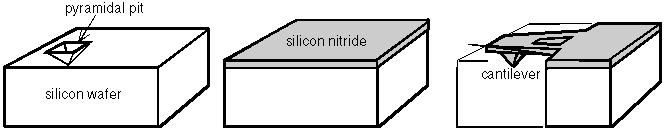
14 The Force Sensor The Tip The Force Sensor The Tip k = Ewt 3 4 l E - Young w width, Comercial Tip radii 3, l - lenght, Module cantiliver o A t - thickness s - SiO 2 and Si 3 N 4 The Force Sensor The Tip The Force Sensor The Tip Diamond-coated tip FIB-sharpened tip Gold-coated Si 3 N 4 tip Tip Resolution Tip Fabrication Pit etching in Si SiN coating Si underetching


15 Nanotube tip Nanotube tip Summary SFM is a powerful tool for surface imaging. SFM covers various techniques that enable many physical measurements of interactions with the surface. SFM interpretation is not straightforward.
Scanning Force Microscopy And Related Techniques
 Scanning Force Microscopy And Related Techniques Danny Porath 2003 With the help of. 1. Yosi Shacham TAU 2. Yossi Rosenwacks TAU 3. Julio Gomez-Herrero UAM 4. Adriana Gil - UAM 5. Serge Lemay - Delft 6.
Lecture 4 Scanning Probe Microscopy (SPM)
") Lecture 4 Scanning Probe Microscopy (SPM) General components of SPM; Tip --- the probe; Cantilever --- the indicator of the tip; Tip-sample interaction --- the feedback system; Scanner --- piezoelectric
Lecture 4 Scanning Probe Microscopy (SPM) General components of SPM; Tip --- the probe; Cantilever --- the indicator of the tip; Tip-sample interaction --- the feedback system; Scanner --- piezoelectric
Module 26: Atomic Force Microscopy. Lecture 40: Atomic Force Microscopy 3: Additional Modes of AFM
 Module 26: Atomic Force Microscopy Lecture 40: Atomic Force Microscopy 3: Additional Modes of AFM 1 The AFM apart from generating the information about the topography of the sample features can be used
Basic Laboratory. Materials Science and Engineering. Atomic Force Microscopy (AFM)
") Basic Laboratory Materials Science and Engineering Atomic Force Microscopy (AFM) M108 Stand: 20.10.2015 Aim: Presentation of an application of the AFM for studying surface morphology. Inhalt 1.Introduction...
Basic Laboratory Materials Science and Engineering Atomic Force Microscopy (AFM) M108 Stand: 20.10.2015 Aim: Presentation of an application of the AFM for studying surface morphology. Inhalt 1.Introduction...
Scanning Probe Microscopy (SPM)
") CHEM53200: Lecture 9 Scanning Probe Microscopy (SPM) Major reference: 1. Scanning Probe Microscopy and Spectroscopy Edited by D. Bonnell (2001). 2. A practical guide to scanning probe microscopy by Park
CHEM53200: Lecture 9 Scanning Probe Microscopy (SPM) Major reference: 1. Scanning Probe Microscopy and Spectroscopy Edited by D. Bonnell (2001). 2. A practical guide to scanning probe microscopy by Park
Scanning Force Microscopy
 Scanning Force Microscopy Roland Bennewitz Rutherford Physics Building 405 Phone 398-3058 roland.bennewitz@mcgill.ca Scanning Probe is moved along scan lines over a sample surface 1 Force Microscopy Data
Instrumentation and Operation
 Instrumentation and Operation 1 STM Instrumentation COMPONENTS sharp metal tip scanning system and control electronics feedback electronics (keeps tunneling current constant) image processing system data
Scanning Tunneling Microscopy
 Scanning Tunneling Microscopy Scanning Direction References: Classical Tunneling Quantum Mechanics Tunneling current Tunneling current I t I t (V/d)exp(-Aφ 1/2 d) A = 1.025 (ev) -1/2 Å -1 I t = 10 pa~10na
NIS: what can it be used for?
 AFM @ NIS: what can it be used for? Chiara Manfredotti 011 670 8382/8388/7879 chiara.manfredotti@to.infn.it Skype: khiaram 1 AFM: block scheme In an Atomic Force Microscope (AFM) a micrometric tip attached
Characterization of MEMS Devices
 MEMS: Characterization Characterization of MEMS Devices Prasanna S. Gandhi Assistant Professor, Department of Mechanical Engineering, Indian Institute of Technology, Bombay, Recap Characterization of MEMS
Atomic Force Microscopy imaging and beyond
 Atomic Force Microscopy imaging and beyond Arif Mumtaz Magnetism and Magnetic Materials Group Department of Physics, QAU Coworkers: Prof. Dr. S.K.Hasanain M. Tariq Khan Alam Imaging and beyond Scanning
Program Operacyjny Kapitał Ludzki SCANNING PROBE TECHNIQUES - INTRODUCTION
 Program Operacyjny Kapitał Ludzki SCANNING PROBE TECHNIQUES - INTRODUCTION Peter Liljeroth Department of Applied Physics, Aalto University School of Science peter.liljeroth@aalto.fi Projekt współfinansowany
Atomic and molecular interactions. Scanning probe microscopy.
 Atomic and molecular interactions. Scanning probe microscopy. Balázs Kiss Nanobiotechnology and Single Molecule Research Group, Department of Biophysics and Radiation Biology 27. November 2013. 2 Atomic
Scanning Probe Microscopy. Amanda MacMillan, Emmy Gebremichael, & John Shamblin Chem 243: Instrumental Analysis Dr. Robert Corn March 10, 2010
 Scanning Probe Microscopy Amanda MacMillan, Emmy Gebremichael, & John Shamblin Chem 243: Instrumental Analysis Dr. Robert Corn March 10, 2010 Scanning Probe Microscopy High-Resolution Surface Analysis
General concept and defining characteristics of AFM. Dina Kudasheva Advisor: Prof. Mary K. Cowman
 General concept and defining characteristics of AFM Dina Kudasheva Advisor: Prof. Mary K. Cowman Overview Introduction History of the SPM invention Technical Capabilities Principles of operation Examples
Scanning Probe Microscopy (SPM)
") Scanning Probe Microscopy (SPM) Scanning Tunneling Microscopy (STM) --- G. Binnig, H. Rohrer et al, (1982) Near-Field Scanning Optical Microscopy (NSOM) --- D. W. Pohl (1982) Atomic Force Microscopy (AFM)
Scanning Probe Microscopy (SPM) Scanning Tunneling Microscopy (STM) --- G. Binnig, H. Rohrer et al, (1982) Near-Field Scanning Optical Microscopy (NSOM) --- D. W. Pohl (1982) Atomic Force Microscopy (AFM)
Imaging Methods: Scanning Force Microscopy (SFM / AFM)
") Imaging Methods: Scanning Force Microscopy (SFM / AFM) The atomic force microscope (AFM) probes the surface of a sample with a sharp tip, a couple of microns long and often less than 100 Å in diameter.
Imaging Methods: Scanning Force Microscopy (SFM / AFM) The atomic force microscope (AFM) probes the surface of a sample with a sharp tip, a couple of microns long and often less than 100 Å in diameter.
Contents. What is AFM? History Basic principles and devices Operating modes Application areas Advantages and disadvantages
 Contents What is AFM? History Basic principles and devices Operating modes Application areas Advantages and disadvantages Figure1: 2004 Seth Copen Goldstein What is AFM? A type of Scanning Probe Microscopy
Intermittent-Contact Mode Force Microscopy & Electrostatic Force Microscopy (EFM)
") WORKSHOP Nanoscience on the Tip Intermittent-Contact Mode Force Microscopy & Electrostatic Force Microscopy (EFM) Table of Contents: 1. Motivation... 1. Simple Harmonic Motion... 1 3. AC-Mode Imaging...
WORKSHOP Nanoscience on the Tip Intermittent-Contact Mode Force Microscopy & Electrostatic Force Microscopy (EFM) Table of Contents: 1. Motivation... 1. Simple Harmonic Motion... 1 3. AC-Mode Imaging...
Point mass approximation. Rigid beam mechanics. spring constant k N effective mass m e. Simple Harmonic Motion.. m e z = - k N z
 Free end Rigid beam mechanics Fixed end think of cantilever as a mass on a spring Point mass approximation z F Hooke s law k N = F / z This is beam mechanics, standard in engineering textbooks. For a rectangular
STM: Scanning Tunneling Microscope
 STM: Scanning Tunneling Microscope Basic idea STM working principle Schematic representation of the sample-tip tunnel barrier Assume tip and sample described by two infinite plate electrodes Φ t +Φ s =
Outline Scanning Probe Microscope (SPM)
") AFM Outline Scanning Probe Microscope (SPM) A family of microscopy forms where a sharp probe is scanned across a surface and some tip/sample interactions are monitored Scanning Tunneling Microscopy (STM)
AFM Outline Scanning Probe Microscope (SPM) A family of microscopy forms where a sharp probe is scanned across a surface and some tip/sample interactions are monitored Scanning Tunneling Microscopy (STM)
SCANNING-PROBE TECHNIQUES OR APPARATUS; APPLICATIONS OF SCANNING-PROBE TECHNIQUES, e.g. SCANNING PROBE MICROSCOPY [SPM]
![SCANNING-PROBE TECHNIQUES OR APPARATUS; APPLICATIONS OF SCANNING-PROBE TECHNIQUES, e.g. SCANNING PROBE MICROSCOPY [SPM]](/thumbs/81/83165631.jpg "SCANNING-PROBE TECHNIQUES OR APPARATUS; APPLICATIONS OF SCANNING-PROBE TECHNIQUES, e.g. SCANNING PROBE MICROSCOPY [SPM]") G01Q SCANNING-PROBE TECHNIQUES OR APPARATUS; APPLICATIONS OF SCANNING-PROBE TECHNIQUES, e.g. SCANNING PROBE MICROSCOPY [SPM] Scanning probes, i.e. devices having at least a tip of nanometre sized dimensions
G01Q SCANNING-PROBE TECHNIQUES OR APPARATUS; APPLICATIONS OF SCANNING-PROBE TECHNIQUES, e.g. SCANNING PROBE MICROSCOPY [SPM] Scanning probes, i.e. devices having at least a tip of nanometre sized dimensions
Scanning Force Microscopy II
 Scanning Force Microscopy II Measurement modes Magnetic force microscopy Artifacts Lars Johansson 1 SFM - Forces Chemical forces (short range) Van der Waals forces Electrostatic forces (long range) Capillary
Introduction to Scanning Probe Microscopy
 WORKSHOP Nanoscience on the Tip Introduction to Scanning Probe Microscopy Table of Contents: 1 Historic Perspectives... 1 2 Scanning Force Microscopy (SFM)... 2 2.1. Contact Mode... 2 2.2. AC Mode Imaging...
Lecture 12: Biomaterials Characterization in Aqueous Environments
 3.051J/20.340J 1 Lecture 12: Biomaterials Characterization in Aqueous Environments High vacuum techniques are important tools for characterizing surface composition, but do not yield information on surface
Microscopie a stilo: principi ed esempi di applicazione
 Microscopie a stilo: principi ed esempi di applicazione Adele Sassella Dipartimento di Scienza dei Materiali Università degli Studi di Milano Bicocca adele.sassella@unimib.it Pavia, 22 aprile 2009 SCANNING
Nitride HFETs applications: Conductance DLTS
 Nitride HFETs applications: Conductance DLTS The capacitance DLTS cannot be used for device trap profiling as the capacitance for the gate will be very small Conductance DLTS is similar to capacitance
MS482 Materials Characterization ( 재료분석 ) Lecture Note 11: Scanning Probe Microscopy. Byungha Shin Dept. of MSE, KAIST
 Lecture Note 11: Scanning Probe Microscopy. Byungha Shin Dept. of MSE, KAIST") 2015 Fall Semester MS482 Materials Characterization ( 재료분석 ) Lecture Note 11: Scanning Probe Microscopy Byungha Shin Dept. of MSE, KAIST 1 Course Information Syllabus 1. Overview of various characterization
2015 Fall Semester MS482 Materials Characterization ( 재료분석 ) Lecture Note 11: Scanning Probe Microscopy Byungha Shin Dept. of MSE, KAIST 1 Course Information Syllabus 1. Overview of various characterization
Techniken der Oberflächenphysik (Techniques of Surface Physics)
") Techniken der Oberflächenphysik (Techniques of Surface Physics) Prof. Yong Lei & Dr. Yang Xu Fachgebiet 3D-Nanostrukturierung, Institut für Physik Contact: yong.lei@tu-ilmenau.de yang.xu@tu-ilmenau.de
Techniken der Oberflächenphysik (Techniques of Surface Physics) Prof. Yong Lei & Dr. Yang Xu Fachgebiet 3D-Nanostrukturierung, Institut für Physik Contact: yong.lei@tu-ilmenau.de yang.xu@tu-ilmenau.de
AFM for Measuring Surface Topography and Forces
 ENB 2007 07.03.2007 AFM for Measuring Surface Topography and Forces Andreas Fery Scanning Probe : What is it and why do we need it? AFM as a versatile tool for local analysis and manipulation Dates Course
Lecture 26 MNS 102: Techniques for Materials and Nano Sciences
 Lecture 26 MNS 102: Techniques for Materials and Nano Sciences Reference: #1 C. R. Brundle, C. A. Evans, S. Wilson, "Encyclopedia of Materials Characterization", Butterworth-Heinemann, Toronto (1992),
Introduction to Scanning Probe Microscopy Zhe Fei
 Introduction to Scanning Probe Microscopy Zhe Fei Phys 590B, Apr. 2019 1 Outline Part 1 SPM Overview Part 2 Scanning tunneling microscopy Part 3 Atomic force microscopy Part 4 Electric & Magnetic force
(Scanning Probe Microscopy)
") (Scanning Probe Microscopy) Ing-Shouh Hwang (ishwang@phys.sinica.edu.tw) Institute of Physics, Academia Sinica, Taipei, Taiwan References 1. G. Binnig, H. Rohrer, C. Gerber, and Weibel, Phys. Rev. Lett.
(Scanning Probe Microscopy) Ing-Shouh Hwang (ishwang@phys.sinica.edu.tw) Institute of Physics, Academia Sinica, Taipei, Taiwan References 1. G. Binnig, H. Rohrer, C. Gerber, and Weibel, Phys. Rev. Lett.
And Manipulation by Scanning Probe Microscope
 Basic 15 Nanometer Scale Measurement And Manipulation by Scanning Probe Microscope Prof. K. Fukuzawa Dept. of Micro/Nano Systems Engineering Nagoya University I. Basics of scanning probe microscope Basic
SOLID STATE PHYSICS PHY F341. Dr. Manjuladevi.V Associate Professor Department of Physics BITS Pilani
 SOLID STATE PHYSICS PHY F341 Dr. Manjuladevi.V Associate Professor Department of Physics BITS Pilani 333031 manjula@bits-pilani.ac.in Characterization techniques SEM AFM STM BAM Outline What can we use
Scanning Tunneling Microscopy
 Scanning Tunneling Microscopy References: 1. G. Binnig, H. Rohrer, C. Gerber, and Weibel, Phys. Rev. Lett. 49, 57 (1982); and ibid 50, 120 (1983). 2. J. Chen, Introduction to Scanning Tunneling Microscopy,
Scanning Tunneling Microscopy
 Scanning Tunneling Microscopy References: 1. G. Binnig, H. Rohrer, C. Gerber, and Weibel, Phys. Rev. Lett. 49, 57 (1982); and ibid 50, 120 (1983). 2. J. Chen, Introduction to Scanning Tunneling Microscopy,
CNPEM Laboratório de Ciência de Superfícies
 Investigating electrical charged samples by scanning probe microscopy: the influence to magnetic force microscopy and atomic force microscopy phase images. Carlos A. R. Costa, 1 Evandro M. Lanzoni, 1 Maria
PY5020 Nanoscience Scanning probe microscopy
 PY500 Nanoscience Scanning probe microscopy Outline Scanning tunnelling microscopy (STM) - Quantum tunnelling - STM tool - Main modes of STM Contact probes V bias Use the point probes to measure the local
Scanning Tunneling Microscopy
 Scanning Tunneling Microscopy A scanning tunneling microscope (STM) is an instrument for imaging surfaces at the atomic level. Its development in 1981 earned its inventors, Gerd Binnig and Heinrich Rohrer
Measurement of hardness, surface potential, and charge distribution with dynamic contact mode electrostatic force microscope
 REVIEW OF SCIENTIFIC INSTRUMENTS VOLUME 70, NUMBER 3 MARCH 1999 Measurement of hardness, surface potential, and charge distribution with dynamic contact mode electrostatic force microscope J. W. Hong,
Instability & Pattering of Thin Polymer Films Prof. R. Mukherjee Department of Chemical Engineering Indian Institute of Technology Kharagpur
 Instability & Pattering of Thin Polymer Films Prof. R. Mukherjee Department of Chemical Engineering Indian Institute of Technology Kharagpur Lecture No#26 Atomic Force Microscope V (Refer Slide Time: 00:34)
Chapter 2 Correlation Force Spectroscopy
 Chapter 2 Correlation Force Spectroscopy Correlation Force Spectroscopy: Rationale In principle, the main advantage of correlation force spectroscopy (CFS) over onecantilever atomic force microscopy (AFM)
INTRODUCTION TO SCA\ \I\G TUNNELING MICROSCOPY
 INTRODUCTION TO SCA\ \I\G TUNNELING MICROSCOPY SECOND EDITION C. JULIAN CHEN Department of Applied Physics and Applied Mathematics, Columbia University, New York OXFORD UNIVERSITY PRESS Contents Preface
AFM Imaging In Liquids. W. Travis Johnson PhD Agilent Technologies Nanomeasurements Division
 AFM Imaging In Liquids W. Travis Johnson PhD Agilent Technologies Nanomeasurements Division Imaging Techniques: Scales Proteins 10 nm Bacteria 1μm Red Blood Cell 5μm Human Hair 75μm Si Atom Spacing 0.4nm
Simple Harmonic Motion and Damping
 Simple Harmonic Motion and Damping Marie Johnson Cabrices Chamblee Charter High School Background: Atomic Force Microscopy, or AFM, is used to characterize materials. It is used to measure local properties,
The most versatile AFM platform for your nanoscale microscopy needs
 The most versatile AFM platform for your nanoscale microscopy needs Atomic Force Microscopy (AFM) for nanometer resolution imaging with electrical, magnetic, thermal, and mechanical property measurement
Today s SPM in Nanotechnology
 Today s SPM in Nanotechnology An introduction for Advanced Applications Qun (Allen) Gu, Ph.D., AFM Scientist, Pacific Nanotechnology IEEE Bay Area Nanotechnology Council, August, 2007 8/17/2015 1 Content
The interpretation of STM images in light of Tersoff and Hamann tunneling model
 The interpretation of STM images in light of Tersoff and Hamann tunneling model The STM image represents contour maps of constant surface LDOS at E F, evaluated at the center of the curvature of the tip.
Studies of the Properties of Designed Nanoparticles Using Atomic Force Microscopy
 Louisiana State University LSU Digital Commons LSU Doctoral Dissertations Graduate School 2016 Studies of the Properties of Designed Nanoparticles Using Atomic Force Microscopy Steve Matthew Deese Louisiana
MAGNETIC FORCE MICROSCOPY
 University of Ljubljana Faculty of Mathematics and Physics Department of Physics SEMINAR MAGNETIC FORCE MICROSCOPY Author: Blaž Zupančič Supervisor: dr. Igor Muševič February 2003 Contents 1 Abstract 3
Scanning Probe Microscopy. EMSE-515 F. Ernst
 Scanning Probe Microscopy EMSE-515 F. Ernst 1 Literature 2 3 Scanning Probe Microscopy: The Lab on a Tip by Ernst Meyer,Ans Josef Hug,Roland Bennewitz 4 Scanning Probe Microscopy and Spectroscopy : Theory,
Integrating MEMS Electro-Static Driven Micro-Probe and Laser Doppler Vibrometer for Non-Contact Vibration Mode SPM System Design
 Tamkang Journal of Science and Engineering, Vol. 12, No. 4, pp. 399 407 (2009) 399 Integrating MEMS Electro-Static Driven Micro-Probe and Laser Doppler Vibrometer for Non-Contact Vibration Mode SPM System
Application of electrostatic force microscopy in nanosystem diagnostics
 Materials Science, Vol., No. 3, 003 Application of electrostatic force microscopy in nanosystem diagnostics TEODOR P. GOTSZALK *, PIOTR GRABIEC, IVO W. RANGELOW 3 Fulty of Microsystem Electronics and Photonics,
Magnetic Force Microscopy practical
 European School on Magnetism 2015 From basic magnetic concepts to spin currents Magnetic Force Microscopy practical Organized by: Yann Perrin, Michal Staňo and Olivier Fruchart Institut NEEL (CNRS & Univ.
Scanning Tunneling Microscopy
 Scanning Tunneling Microscopy References: 1. G. Binnig, H. Rohrer, C. Gerber, and Weibel, Phys. Rev. Lett. 49, 57 (1982); and ibid 50, 120 (1983). 2. J. Chen, Introduction to Scanning Tunneling Microscopy,
SUPPLEMENTARY NOTES Supplementary Note 1: Fabrication of Scanning Thermal Microscopy Probes
 SUPPLEMENTARY NOTES Supplementary Note 1: Fabrication of Scanning Thermal Microscopy Probes Fabrication of the scanning thermal microscopy (SThM) probes is summarized in Supplementary Fig. 1 and proceeds
Enrico Gnecco Department of Physics. University of Basel, Switzerland
 AOSCIECES AD AOTECHOOGIES anotribology - Enrico Gnecco AOTRIBOOGY Enrico Gnecco Department of Physics. University of Basel, Switzerland Keywords: Atomic stick-slip, Friction force microscopy, oad dependence
Scanning Probe Microscopy. L. J. Heyderman
 1 Scanning Probe Microscopy 2 Scanning Probe Microscopy If an atom was as large as a ping-pong ball......the tip would have the size of the Matterhorn! 3 Magnetic Force Microscopy Stray field interaction
Magnetic Force Microscopy (MFM) F = µ o (m )H
 F = µ o (m )H") Magnetic Force Microscopy (MFM) F = µ o (m )H 1. MFM is based on the use of a ferromagnetic tip as a local field sensor. Magnetic interaction between the tip and the surface results in a force acting on
Magnetic Force Microscopy (MFM) F = µ o (m )H 1. MFM is based on the use of a ferromagnetic tip as a local field sensor. Magnetic interaction between the tip and the surface results in a force acting on
Introduction to Scanning Tunneling Microscopy
 Introduction to Scanning Tunneling Microscopy C. JULIAN CHEN IBM Research Division Thomas J. Watson Research Center Yorktown Heights, New York New York Oxford OXFORD UNIVERSITY PRESS 1993 CONTENTS List
Review. Surfaces of Biomaterials. Characterization. Surface sensitivity
 Surfaces of Biomaterials Three lectures: 1.23.05 Surface Properties of Biomaterials 1.25.05 Surface Characterization 1.27.05 Surface and Protein Interactions Review Bulk Materials are described by: Chemical
Reducing dimension. Crystalline structures
 Reducing dimension 2D surfaces, interfaces and quantum wells 1D carbon nanotubes, quantum wires and conducting polymers 0D nanocrystals, nanoparticles, lithographically patterned quantum dots Crystalline
Atomic Force Microscopy (AFM) Part I
 Part I") Atomic Force Microscopy (AFM) Part I CHEM-L2000 Eero Kontturi 6 th March 2018 Lectures on AFM Part I Principles and practice Imaging of native materials, including nanocellulose Part II Surface force measurements
Atomic Force Microscopy (AFM) Part I CHEM-L2000 Eero Kontturi 6 th March 2018 Lectures on AFM Part I Principles and practice Imaging of native materials, including nanocellulose Part II Surface force measurements
Characterization Tools
 Lectures in Nanoscience & Technology Characterization Tools K. Sakkaravarthi Department of Physics National Institute of Technology Tiruchirappalli 620 015 Tamil Nadu India sakkaravarthi@nitt.edu ksakkaravarthi.weebly.com
= 6 (1/ nm) So what is probability of finding electron tunneled into a barrier 3 ev high?
 So what is probability of finding electron tunneled into a barrier 3 ev high?") STM STM With a scanning tunneling microscope, images of surfaces with atomic resolution can be readily obtained. An STM uses quantum tunneling of electrons to map the density of electrons on the surface
STM STM With a scanning tunneling microscope, images of surfaces with atomic resolution can be readily obtained. An STM uses quantum tunneling of electrons to map the density of electrons on the surface
Experimental methods in physics. Local probe microscopies I
 Experimental methods in physics Local probe microscopies I Scanning tunnelling microscopy (STM) Jean-Marc Bonard Academic year 09-10 1. Scanning Tunneling Microscopy 1.1. Introduction Image of surface
Supporting Information
 Supporting Information Analysis Method for Quantifying the Morphology of Nanotube Networks Dusan Vobornik*, Shan Zou and Gregory P. Lopinski Measurement Science and Standards, National Research Council
Scanning Probe Microscopy
 1 Scanning Probe Microscopy Dr. Benjamin Dwir Laboratory of Physics of Nanostructures (LPN) Benjamin.dwir@epfl.ch PH.D3.344 Outline: Introduction: What is SPM, history STM AFM Image treatment Advanced
A CONTROL SYSTEMS PERSPECTIVE ON NANOINTERROGATION
 A CONTROL SYSTEMS PERSPECTIVE ON NANOINTERROGATION Scanning Probe Microscopy At the 1959 annual meeting of the American Physical Society, Richard Feynman gave a seminal talk titled There s Plenty of Room
tip of a current tip and the sample. Components: 3. Coarse sample-to-tip isolation system, and
 SCANNING TUNNELING MICROSCOPE Brief history: Heinrich Rohrer and Gerd K. Binnig, scientists at IBM's Zurich Research Laboratory in Switzerland, are awarded the 1986 Nobel Prize in physicss for their work
3.052 Nanomechanics of Materials and Biomaterials Thursday 02/22/07 Prof. C. Ortiz, MIT-DMSE
 I LECTURE 5: AFM IMAGING Outline : LAST TIME : HRFS AND FORCE-DISTANCE CURVES... 2 ATOMIC FORCE MICROSCOPY : GENERAL COMPONENTS AND FUNCTIONS... 3 Deflection vs. Height Images... 4 3D Plots and 2D Section
Understanding the properties and behavior of groups of interacting atoms more than simple molecules
 Condensed Matter Physics Scratching the Surface Understanding the properties and behavior of groups of interacting atoms more than simple molecules Solids and fluids in ordinary and exotic states low energy
CHAPTER 4 DESIGN AND ANALYSIS OF CANTILEVER BEAM ELECTROSTATIC ACTUATORS
 61 CHAPTER 4 DESIGN AND ANALYSIS OF CANTILEVER BEAM ELECTROSTATIC ACTUATORS 4.1 INTRODUCTION The analysis of cantilever beams of small dimensions taking into the effect of fringing fields is studied and
Dopant Concentration Measurements by Scanning Force Microscopy
 73.40L Scanning Microsc. Microanal. Microstruct. 551 Classification Physics Abstracts - - 61.16P 73.00 Dopant Concentration Measurements by Scanning Force Microscopy via p-n Junctions Stray Fields Jacopo
bio-molecular studies Physical methods in Semmelweis University Osváth Szabolcs
 Physical methods in bio-molecular studies Osváth Szabolcs Semmelweis University szabolcs.osvath@eok.sote.hu Light emission and absorption spectra Stokes shift is the difference (in wavelength or frequency
From Last Time. Mon. Nov 8 Phy107 Lecture 26
 From Last Time Particle can exist in different quantum states, having Different energy Different momentum Different wavelength The quantum wavefunction describes wave nature of particle. Square of the
Other SPM Techniques. Scanning Probe Microscopy HT10
 Other SPM Techniques Scanning Near-Field Optical Microscopy (SNOM) Scanning Capacitance Microscopy (SCM) Scanning Spreading Resistance Microscopy (SSRM) Multiprobe techniques Electrostatic Force Microscopy,
Ecole Franco-Roumaine : Magnétisme des systèmes nanoscopiques et structures hybrides - Brasov, Modern Analytical Microscopic Tools
 1. Introduction Solid Surfaces Analysis Group, Institute of Physics, Chemnitz University of Technology, Germany 2. Limitations of Conventional Optical Microscopy 3. Electron Microscopies Transmission Electron
Institute for Electron Microscopy and Nanoanalysis Graz Centre for Electron Microscopy
 Institute for Electron Microscopy and Nanoanalysis Graz Centre for Electron Microscopy Micromechanics Ass.Prof. Priv.-Doz. DI Dr. Harald Plank a,b a Institute of Electron Microscopy and Nanoanalysis, Graz
CHARACTERIZATION of NANOMATERIALS KHP
 CHARACTERIZATION of NANOMATERIALS Overview of the most common nanocharacterization techniques MAIN CHARACTERIZATION TECHNIQUES: 1.Transmission Electron Microscope (TEM) 2. Scanning Electron Microscope
Electrostatic Force Microscopy (EFM)
") 6 Electrostatic Force Microscopy (EFM) Masakazu Nakamura and Hirofumi Yamada 1 Department of Electronics and Mechanical Engineering, Faculty of Engineering, Chiba University, 1-33 Yayoi-cho, Inage-ku,
6 Electrostatic Force Microscopy (EFM) Masakazu Nakamura and Hirofumi Yamada 1 Department of Electronics and Mechanical Engineering, Faculty of Engineering, Chiba University, 1-33 Yayoi-cho, Inage-ku,
Electrical Characterization with SPM Application Modules
 Electrical Characterization with SPM Application Modules Metrology, Characterization, Failure Analysis: Data Storage Magnetoresistive (MR) read-write heads Semiconductor Transistors Interconnect Ferroelectric
Scanning capacitance spectroscopy of an Al x Ga 1Àx NÕGaN heterostructure field-effect transistor structure: Analysis of probe tip effects
 Scanning capacitance spectroscopy of an Al x Ga 1Àx NÕGaN heterostructure field-effect transistor structure: Analysis of probe tip effects D. M. Schaadt and E. T. Yu a) Department of Electrical and Computer
EXPLORING SCANNING PROBE MICROSCOPY WITH MATHEMATICA
 EXPLORING SCANNING PROBE MICROSCOPY WITH MATHEMATICA Dror Sarid University of Arizona A WILEY-1NTERSCIENCE PUBLICATION JOHN WILEY & SONS, INC. New York Chichester Weinheim Brisbane Singapore Toronto CONTENTS
Nanostructure. Materials Growth Characterization Fabrication. More see Waser, chapter 2
 Nanostructure Materials Growth Characterization Fabrication More see Waser, chapter 2 Materials growth - deposition deposition gas solid Physical Vapor Deposition Chemical Vapor Deposition Physical Vapor
3.052 Nanomechanics of Materials and Biomaterials Thursday 02/15/07 Prof. C. Ortiz, MIT-DMSE I LECTURE 4: FORCE-DISTANCE CURVES
 I LECTURE 4: FORCE-DISTANCE CURVES Outline : LAST TIME : ADDITIONAL NANOMECHANICS INSTRUMENTATION COMPONENTS... 2 PIEZOS TUBES : X/Y SCANNING... 3 GENERAL COMPONENTS OF A NANOMECHANICAL DEVICE... 4 HIGH
Softlithography and Atomic Force Microscopy
 Praktikum I, Autumn Semester 2008/09 Experiment 13/14; 03.12.2008 Softlithography and Atomic Force Microscopy Authors: Claudio Zihlmann (zclaudio@student.ethz.ch) and Philippe Knüsel (pknuesel@student.ethz.ch)
MSE 321 Structural Characterization
 Auger Spectroscopy Auger Electron Spectroscopy (AES) Scanning Auger Microscopy (SAM) Incident Electron Ejected Electron Auger Electron Initial State Intermediate State Final State Physical Electronics
Chapter 10. Nanometrology. Oxford University Press All rights reserved.
 Chapter 10 Nanometrology Oxford University Press 2013. All rights reserved. 1 Introduction Nanometrology is the science of measurement at the nanoscale level. Figure illustrates where nanoscale stands
Effects of environment on friction
 Summer Undergraduate Research Exchange Program 2004 (SURE) Effects of environment on friction Man Lan Fun Materials Science and Engineering, Physics Department CUHK Supervisor: Prof. Y.W. Chung Materials
Fundamentals of Atomic Force Microscopy Part 2: Dynamic AFM Methods
 Fundamentals of tomic Force Microscopy Part 2: Dynamic FM Methods Week 2, Lecture 5 ttractive and repulsive regimes and phase contrast in amplitude modulation FM rvind Raman Mechanical Engineering Birck
MSE 321 Structural Characterization
 Auger Spectroscopy Auger Electron Spectroscopy (AES) Scanning Auger Microscopy (SAM) Incident Electron Ejected Electron Auger Electron Initial State Intermediate State Final State Physical Electronics
Scanning Probe Microscopies (SPM)
") Scanning Probe Microscopies (SPM) Nanoscale resolution af objects at solid surfaces can be reached with scanning probe microscopes. They allow to record an image of the surface atomic arrangement in direct
Scanning Probe Microscopies (SPM) Nanoscale resolution af objects at solid surfaces can be reached with scanning probe microscopes. They allow to record an image of the surface atomic arrangement in direct
Chapter 2 Scanning Probe Microscopy Principle of Operation, Instrumentation, and Probes
 Chapter 2 Scanning Probe Microscopy Principle of Operation, Instrumentation, and Probes Bharat Bhushan and Othmar Marti Abstract Since the introduction of the STM in 1981 and the AFM in 1985, many variations
Santosh Devasia Mechanical Eng. Dept., UW
 Nano-positioning Santosh Devasia Mechanical Eng. Dept., UW http://faculty.washington.edu/devasia/ Outline of Talk 1. Why Nano-positioning 2. Sensors for Nano-positioning 3. Actuators for Nano-positioning
CBSE PHYSICS QUESTION PAPER (2005)
") CBSE PHYSICS QUESTION PAPER (2005) (i) (ii) All questions are compulsory. There are 30 questions in total. Questions 1 to 8 carry one mark each, Questions 9 to 18 carry two marks each, Question 19 to 27
CBSE PHYSICS QUESTION PAPER (2005) (i) (ii) All questions are compulsory. There are 30 questions in total. Questions 1 to 8 carry one mark each, Questions 9 to 18 carry two marks each, Question 19 to 27
Scanning Tunneling Microscopy and its Application
 Chunli Bai Scanning Tunneling Microscopy and its Application With 181 Figures SHANGHAI SCIENTIFIC & TECHNICAL PUBLISHERS Jpl Springer Contents 1. Introduction 1 1.1 Advantages of STM Compared with Other
3.052 Nanomechanics of Materials and Biomaterials Thursday 02/22/07 Prof. C. Ortiz, MIT-DMSE
 I LECTURE 5: AFM IMAGING Outline : LAST TIME : HRFS AND FORCE-DISTANCE CURVES... 2 ATOMIC FORCE MICROSCOPY : GENERAL COMPONENTS AND FUNCTIONS... 3 Deflection vs. Height Images... 4 3D Plots and 2D Section