AKD5381-B AK5381 Evaluation Board Rev.1
|
|
|
- Aubrey Lawson
- 6 years ago
- Views:
Transcription
1 [AKD5381-] AKD5381- AK5381 Evaluation oar Rev.1 GENERAL DECRIPTION AKD5381- is an evaluation boar for the igital auio 4bit 96k A/D converter, AK5381. AKD5381- has analog input circuits an a igital interface transmitter,an can achieve the interface with igital auio systems via opt-connector. Orering guie AKD AK5381 Evaluation oar DIT (AK4114) with optical output UNCTION VA,VD AGND,DGND LIN RIN AK5381 AK4114 (DIT) Opt Out DP Data 10pin Heaer igure 1. AKD5381- lock Diagram * Circuit iagram an PC layout are attache at the en of this manual
2 [AKD5381-] 1. Evaluation oar Manual Operation sequence 1) et up the power supply lines. [VA] (re) =.7 5.5V or 15V : for VA of AK5381 (typ. 5.0V) [VD] (orange) =.7 5.5V : for VD of AK5381, 74HC14 (typ. 5.0V) [VCC] (re) = 3.3V : for AK4114 [AGND] (black) = 0V : for analog groun [DGND] (black) = 0V : for logic groun Each supply line shoul be istribute from the power supply unit. ) et up the evaluation moe, jumper pins an DIP switches. (ee the followings.) 3) Power on. The AK5381 an AK4114 shoul be reset once bringing W = L upon power-up. Evaluation moe (1) lave Moe (1-1) A/D evaluation using DIT function of AK4114 PORT (DIT) is use. DIT generates auio bi-phase signal from receive ata an which is output through optical connector (TOTX141). It is possible to connect s D/A converter evaluation boars on the igital-amplifier, which equips DIR input. Nothing shoul be connecte to PORT1 (DP). JP5 MCLK (1-) All interface signals incluing master clock are fe externally. PORT1 (DP) is use. All interface signals (MCLK, CLK, LRCK) are provie to the AK5381 through PORT1. JP5 (MCLK) shoul be open. The DI1 of W1 (MODE) shoul be set to H. JP5 MCLK - -
3 [AKD5381-] () Master Moe (-1) A/D evaluation using DIT function of AK4114 PORT (DIT) is use. DIT generates auio bi-phase signal from receive ata an which is output through optical connector (TOTX141). It is possible to connect s D/A converter evaluation boars on the igital-amplifier, which equips DIR input. Nothing shoul be connecte to PORT1 (DP). The DI1 of W1 (MODE) shoul be set to H. JP5 MCLK (-) Master clock is fe externally. PORT1 (DP) is use. MCLK is provie to the AK5381 through PORT1. JP5 (MCLK) shoul be open. The DI1 of W1 (MODE) shoul be set to H. JP5 MCLK Other jumper pins set up 1. JP1 (GND) : Analog groun an Digital groun OPEN : eparate. HORT : Common. (The connector DGND can be open.) <Default>. JP (CK1) : etting of CK1 pin for AK5381 H : Master moe L : lave moe <Default> 3. JP3 (VA) : elect VA for AK5381 VA : upply from VA connector <Default> REG : upply from regulator. VA connector shoul be supplie 15V. 4. JP4 (VD) : elect VD for AK5381 VA : upply from VA connector VD : upply from VD connector <Default> - 3 -
4 [AKD5381-] DIP witch set up [W1] (MODE1): etting the evaluation moe for AK5381 an AK4114 ON is H, O is L. CK1 shoul be set by JP. No. Name O ( L ) ON ( H ) 1 CK0 ee Table CK 3 DI M justifie I Compatible 4 DI1 AK4114 Master moe AK4114 lave moe Table 1. Moe etting CK CK1 CK0 Input Level HP Master/lave MCLK CLK L L L CMO ON lave 56/384/51/768fs 48fs or 3fs L L H CMO O lave 56/384/51/768fs 48fs or 3fs L H L CMO ON Master 56fs ( 96k) 64fs L H H CMO ON Master 51fs ( 48k) 64fs H L L TTL ON lave 56/384/51/768fs 48fs or 3fs H L H Reserve H H L CMO ON Master 384fs ( 96k) 64fs H H H CMO ON Master 768fs ( 48k) 64fs Table. Moe etting of AK5381 Note: AK4114 oes not support MCLK=384fs/51fs/768fs. PORT1 (DP) shoul be use when MCLK=384fs/51fs/768fs. The function of the toggle W Upper-sie is H an lower-sie is L. [W] (PDN): Resets the AK5381 an AK4114. Keep H uring normal operation
5 [AKD5381-] Analog Input Circuits Analog signal is input via J1(RIN) an J(LIN) of RCA connectors. J1 RIN C1 10u AINR J LIN C 10u AINL igure. Analog Input circuits * assumes no responsibility for the trouble when using the circuit examples
6 [AKD5381-] MEAUREMENT REULT [Measurement conition] Measurement unit : Auio Precision, ystem Two Cascae MCLK : 56fs CLK : 64fs fs : 48k, 96k it : 4bit Power upply : VA = VD = 5.0V (Using regulator) Interface : DIT Temperature : Room Parameter Result (Lch / Rch) Unit ADC Analog Input Characteristics: /(ND) ( 1 Input) fs=48k fs=96k 89.0 / / 86. D-Range ( 60 Input) fs=48k, A-weighte fs=96k 10.7 / / 99. /N fs=48k, A-weighte fs=96k 10.8 / / 99.4 Interchannel Isolation 13.6 /
7 [AKD5381-] [ADC Plot : fs=48k] AK5381 THDN vs. Input Level VA=VD=5.0V, fs=48k, fin=1k r igure 1. THDN vs. Input Level AK5381 THDN vs. Input requency VA=VD=5.0V, fs=48k, Input=-1r k k 5k 10k 0k igure. THDN vs. Input requency - 7 -
8 [AKD5381-] 0 AK5381 Linearity VA=VD=5.0V, fs=48k, fin=1k r igure 3. Linearity -0.5 AK5381 requency Response VA=VD=5.0V, fs=48k, Input=-1r k k 5k 10k 0k igure 4. requency Response - 8 -
9 [AKD5381-] AK5381 Crosstalk VA=VD=5.0V, fs=48k, Input=-1r k k 5k 10k 0k igure 5. Crosstalk AK5381 T Plot VA=VD=5.0V, fs=48k, Input=-1r, fin=1k k k 5k 10k 0k igure 6. T Plot - 9 -
10 [AKD5381-] AK5381 T Plot VA=VD=5.0V, fs=48k, Input=-60r, fin=1k k k 5k 10k 0k igure 7. T Plot AK5381 T Plot VA=VD=5.0V, fs=48k, fin=none k k 5k 10k 0k igure 8. T Plot
11 [AKD5381-] [ADC Plot : fs=96k] AK5381 THDN vs. Input Level VA=VD=5.0V, fs=96k, fin=1k r igure 9. THDN vs. Input Level AK5381 THDN vs. Input requency VA=VD=5.0V, fs=96k, Input=-1r k k 5k 10k 0k 40k igure 10. THDN vs. Input requency
12 [AKD5381-] 0 AK5381 Linearity VA=VD=5.0V, fs=96k, fin=1k r igure 11. Linearity AK5381 requency Response VA=VD=5.0V, fs=96k, Input=-1r k k 5k 10k 0k 40k igure 1. requency Response - 1 -
13 [AKD5381-] AK5381 Crosstalk VA=VD=5.0V, fs=96k, Input=-1r k k 5k 10k 0k 40k igure 13. Crosstalk AK5381 T Plot VA=VD=5.0V, fs=96k, Input=-1r, fin=1k k k 5k 10k 0k 40k igure 14. T Plot
14 [AKD5381-] AK5381 T Plot VA=VD=5.0V, fs=96k, Input=-60r, fin=1k k k 5k 10k 0k 40k igure 15. T Plot AK5381 T Plot VA=VD=5.0V, fs=96k, fin=none k k 5k 10k 0k 40k igure 16. T Plot
15 [AKD5381-] Revision History Date Manual oar Reason Contents (YY/MM/DD) Revision Revision 04/05/14 KM irst Eition 05/01/14 KM oar Name Change AKD5381 Rev. AKD5381- Rev.0 Circuit Change The information on AK5357 was remove. 06/04/4 KM Error Correction oar Rev: 0 1 IMPORTANT NOTICE These proucts an their specifications are subject to change without notice. efore consiering any use or application, consult the Asahi Kasei Microsystems Co., Lt. () sales office or authorize istributor concerning their current status. assumes no liability for infringement of any patent, intellectual property, or other right in the application or use of any information containe herein. Any export of these proucts, or evices or systems containing them, may require an export license or other official approval uner the law an regulations of the country of export pertaining to customs an tariffs, currency exchange, or strategic materials. proucts are neither intene nor authorize for use as critical components in any safety, life support, or other hazar relate evice or system, an assumes no responsibility relating to any such use, except with the express written consent of the Representative Director of. As use here: (a) A hazar relate evice or system is one esigne or intene for life support or maintenance of safety or for applications in meicine, aerospace, nuclear energy, or other fiels, in which its failure to function or perform may reasonably be expecte to result in loss of life or in significant injury or amage to person or property. (b) A critical component is one whose failure to function or perform may reasonably be expecte to result, whether irectly or inirectly, in the loss of the safety or effectiveness of the evice or system containing it, an which must therefore meet very high stanars of performance an reliability. It is the responsibility of the buyer or istributor of an prouct who istributes, isposes of, or otherwise places the prouct with a thir party to notify that party in avance of the above content an conitions, an the buyer or istributor agrees to assume any an all responsibility an liability for an hol harmless from any an all claims arising from the use of sai prouct in the absence of such notification
16 A C D E E JP1 GND DGND AGND E J1 RIN C1 10u VD D J LIN C 10u U1 1 AINR AINL CK0 CK W1 DI1 MODE CK0 CK DI DI RP1 47k D L 3 CK1 DI 14 DI0 C VA 1 C10 47u C7 0.1u T1 JP3 NJM78M05A REG 1 IN GND OUT 3 C8 47u VA REG C9 0.1u VD REG JP CK1 H R3 5.1 JP4 VD VD VA C3 C4.u 0.1u C5 10u C6 0.1u C11 C1 10u 0.1u VCOM AGND VA VD DGND AK5381 PDN 13 CLK 1 MCLK 11 LRCK 10 DTO 9 R1 51 R 51 R4 51 R5 51 CLK MCLK LRCK DTO C 1 C13 47u VD 1 D1 HU119 R6 10k UA 74HC14 U 74HC14 L H PDN W PDN 3 1 C14 0.1u 6 5 VD UC 74HC14 for 74HC C15 0.1u UD 74HC UE 74HC14 A 1 13 A A U 74HC14 C D Title AKD5381- ize Document Number Rev A3 AK Date: Monay, April 4, 006 heet 1 of E
17 A C D E E REG VCC E C17 10u C16 47u C18 0.1u C u D 48 RX3 NC RX 45 D 1 IP0 INT0 36 NC OCK0 35 DI0 3 DI0 OCK1 34 MCLK C DI TET DI1 NC DI IP1 P/N CM1 33 CM0 3 PDN 31 PDN 30 XTI XTO 9 DAUX 8 CLK LRCK DTO MCLK CLK LRCK DTO PORT DP C 10 XTL0 MCKO 7 11 XTL1 ICK 6 C4 10u C5 10u A A C6 0.1u TVDD DV TX0 TX1 OUT COUT UOUT VOUT DVDD DV MCKO1 TET1 44 RX1 NC 43 4 RX0 AV 41 VCOM 40 R 39 AVDD INT1 U3 AK VIN 14 DTO 5 15 LRCK C0 10p X1 1.88M C1 10p 18 C 0.1u C3 0.1u 3 4 JP5 MCLK PORT IN 3 VCC GND 1 DIT C D Title AKD5381- ize Document Number Rev A3 AK Date: Monay, April 4, 006 heet of E A
18
19
20
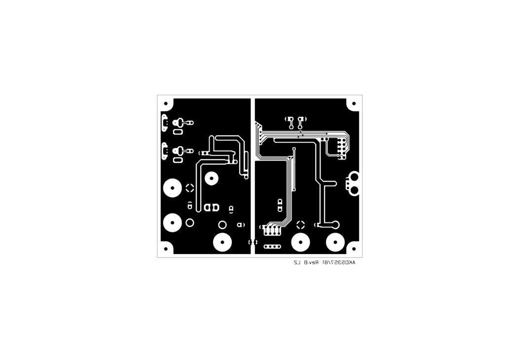
AKD5357-B AK5357 Evaluation Board Rev.2
 [AKD5357-] AKD5357- AK5357 Evaluation oar Rev. GENERAL DECRIPTION AKD5357- is an evaluation boar for the igital auio 4bit 96k A/D converter, AK5357. AKD5357- has analog input circuits an a igital interface
[AKD5384] AK5384 Evaluation Board Rev.A
![[AKD5384] AK5384 Evaluation Board Rev.A](/thumbs/85/91582140.jpg "[AKD5384] AK5384 Evaluation Board Rev.A") HI KI [K8] K8 K8 valuation oar Rev. GNRL RIPTION K8 is an evaluation boar for the igital auio bit 9k ch / converter, K8. The K8 inclues the input circuit an also has a igital interface transmitter. urther,
HI KI [K8] K8 K8 valuation oar Rev. GNRL RIPTION K8 is an evaluation boar for the igital auio bit 9k ch / converter, K8. The K8 inclues the input circuit an also has a igital interface transmitter. urther,
AKD4554-E Evaluation board Rev.0 for AK4554
 SHI KSI [K4554] K4554- valuation boar Rev.0 for K4554 GNRL SRIPTION K4554- is an evaluation boar for the portable igital auio 6bit / an / converter, K4554. The K4554- can evaluate / converter an / converter
[AKD9-] Evaluation oar Diagram oar Diagram J0 T T J00 J00 J0 J0 J00 T W0 J0 U U J00 W00 W00 W0 J0 PORT PORT igure. AKD9-A oar Diagram Description () U
![[AKD9-] Evaluation oar Diagram oar Diagram J0 T T J00 J00 J0 J0 J00 T W0 J0 U U J00 W00 W00 W0 J0 PORT PORT igure. AKD9-A oar Diagram Description () U](/thumbs/82/85828994.jpg "[AKD9-] Evaluation oar Diagram oar Diagram J0 T T J00 J00 J0 J0 J00 T W0 J0 U U J00 W00 W00 W0 J0 PORT PORT igure. AKD9-A oar Diagram Description () U") [AKD9-] AK9 Evaluation oar Rev.0 GENERAL DECRIPTION The AKD9- is an evaluation boar for AK9, which is bit,8k,ch ADC. The AKD9- is inclues the the analog input circuit an also has a igital interface transmitter.
[AKD9-] AK9 Evaluation oar Rev.0 GENERAL DECRIPTION The AKD9- is an evaluation boar for AK9, which is bit,8k,ch ADC. The AKD9- is inclues the the analog input circuit an also has a igital interface transmitter.
[AKD4565] Evaluation board Rev.A for AK4565
![[AKD4565] Evaluation board Rev.A for AK4565](/thumbs/88/115625650.jpg "[AKD4565] Evaluation board Rev.A for AK4565") [KD4565] KD4565 Evaluation boar Rev. for K4565 GENERL DESCRIPTION KD4565 is an evaluation boar for the 0bit ch /D an D/ converter, K4565. The KD4565 can evaluate /D converter an D/ converter separately
[KD4565] KD4565 Evaluation boar Rev. for K4565 GENERL DESCRIPTION KD4565 is an evaluation boar for the 0bit ch /D an D/ converter, K4565. The KD4565 can evaluate /D converter an D/ converter separately
EQ-730L Linear Hall IC
 Distributed By: 9 Industrial Road, San Carlos, CA, 94070 USA GMW Associates PHONE: +1 60-802-8292 FAX: +1 60-802-8298 EMAIL: sales@gmw.com WEB: www.gmw.com EQ-70L Linear Hall IC Features Analog output
INTEGRATED CIRCUITS. For a complete data sheet, please also download:
 INTEGRATED CIRCUITS DATA SEET For a complete ata sheet, please also ownloa: The IC6 74C/CT/CU/CMOS ogic Family Specifications The IC6 74C/CT/CU/CMOS ogic Package Information The IC6 74C/CT/CU/CMOS ogic
TC4013BP,TC4013BF,TC4013BFN
 TOSHIBA CMOS Digital Integrated Circuit Silicon Monolithic TC4013BP,TC4013BF,TC4013BFN TC4013B Dual D-Type Flip Flop TC4013B contains two independent circuits of D type flip-flop. The input level applied
TC74VHCT573AF,TC74VHCT573AFW,TC74VHCT573AFT
 TOSHIBA CMOS igital Integrated Circuit Silicon Monolithic TC74HCT573AF/AFW/AFT TC74HCT573AF,TC74HCT573AFW,TC74HCT573AFT Octal -Type Latch with 3-State Output The TC74HCT573A is an advanced high speed CMOS
Low Voltage 400 MHz Quad 2:1 Mux with 3 ns Switching Time ADG774A
 a FEATURE Bandwidth >4 MHz Low Insertion Loss and On Resistance: 2.2 Typical On-Resistance Flatness.3 Typical ingle 3 V/5 upply Operation Very Low istortion:
1 pc Charge Injection, 100 pa Leakage, CMOS 5 V/+5 V/+3 V Quad SPST Switches ADG611/ADG612/ADG613
 a FEATURE 1 pc Charge Injection 2.7 V to 5.5 V ual upply +2.7 V to +5.5 V ingle upply Automotive Temperature Range 4 C to +125 C 1 pa Max @ 25 C Leakage Currents 85 On-Resistance Rail-to-Rail witching
SN74LS175MEL. Quad D Flip Flop LOW POWER SCHOTTKY
 uad Flip Flop The LSTTL/MSI SN74LS75 is a high speed uad Flip-Flop. The device is useful for general flip-flop requirements where clock and clear inputs are common. The information on the inputs is stored
1 pc Charge Injection, 100 pa Leakage CMOS 5 V/5 V/3 V 4-Channel Multiplexer ADG604
 a FEATURES 1 pc Charge Injection (Over the Full Signal Range) 2.7 V to 5.5 V ual Supply 2.7 V to 5.5 ingle Supply Automotive Temperature Range: 4 C to +125 C 1 pa Max @ 25 C Leakage Currents 85 Typ On
Linear Regulator Application Information
 Linear Regulator Application Information IC Product Name BD00IA5WEFJ Topology LDO Linear Regulator Voltage source Input Output 1 2.4V to 5.5V 1.0V, 500mA *1 2 2.4V to 5.5V 1.2V, 500mA *1 3 2.4V to 5.5V
FUNCTION. Write/Read RAM: Access to PRAM, CRAM, OFFRAM and Registers Digital Audio Interface - Test pin header. Regulator 1.2V.
 [K-] K- K Evaluation oard Rev.0 GENERL ESRIPTION The K- is an evaluation kit for the K; a digital signal processor (SP) with channels digital data interface. It realizes an easy evaluation of the audio
TC74VHC574F,TC74VHC574FW,TC74VHC574FT,TC74VHC574FK
 TOSHIBA CMOS igital Integrated Circuit Silicon Monolithic TC74VHC574F/FW/FT/FK TC74VHC574F,TC74VHC574FW,TC74VHC574FT,TC74VHC574FK Octal -Type Flip Flop with 3-State Output The TC74VHC574 is advanced high
TOSHIBA CMOS Digital Integrated Circuit Silicon Monolithic TC7SG02FU IN A GND
 TOSHIBA CMOS Digital Integrated Circuit Silicon Monolithic TC7SG02FU 2 Input NOR Gate Features High-level output current: I OH /I OL = ±8 ma (min) at = 3.0 High-speed operation: t pd = 2.4 ns (typ.) at
GR16. Technical Manual. 10 M SPS, 16-bit Analog Signal Digitizer up to 8MB FIFO
 GR M SPS, -bit Analog Signal Digitizer up to MB FIFO Technical Manual 90 th Street, Davis, CA 9, USA Tel: 0--00 Fax: 0--0 Email: sales@tern.com web site: www.tern.com COPYRIGHT GR, EL, Grabber, and A-Engine
74LVC374 Octal D-type flip-flop; positive edge-trigger (3-State) INTEGRATED CIRCUITS
 INTEGRATED CIRCUITS") INTEGRATE CIRCUITS Octal -type flip-flop; positive edge-trigger (3-State) Supersedes data of February 1996 IC24 ata Handbook 1997 Mar 12 FEATURES Wide supply voltage range of 1.2V to 3.6V In accordance
INTEGRATE CIRCUITS Octal -type flip-flop; positive edge-trigger (3-State) Supersedes data of February 1996 IC24 ata Handbook 1997 Mar 12 FEATURES Wide supply voltage range of 1.2V to 3.6V In accordance
TC74VHC573F,TC74VHC573FW,TC74VHC573FT,TC74VHC573FK
 TOSHIBA CMOS igital Integrated Circuit Silicon Monolithic TC74VHC573F/FW/FT/FK TC74VHC573F,TC74VHC573FW,TC74VHC573FT,TC74VHC573FK Octal -Type Latch with 3-State Output The TC74VHC573 is an advanced high
Low Capacitance, Low Charge Injection, ±15 V/+12 V icmos Quad SPST Switches ADG1212-EP
 Enhanced Product Low Capacitance, Low Charge Injection, ±15 V/+12 V icmo Quad PT witches FEATURE 1 pf off capacitance 2.6 pf on capacitance
ASAHI Hall Effect ICs
 ASAHI Hall Effect ICs 2014-15 IMPORTANT NOTICE These products and their specifications are subject to change without notice. When you consider any use or application of these products, please make inquiries
74HC1GU04GV. 1. General description. 2. Features. 3. Ordering information. Marking. 5. Functional diagram. Inverter
 Rev. 5 1 July 27 Product data sheet 1. General description 2. Features 3. Ordering information The is a high-speed Si-gate CMOS device. It provides an inverting single stage function. The standard output
7-stage binary ripple counter
 Rev. 9 28 April 2016 Product data sheet 1. General description The is a with a clock input (CP), an overriding asynchronous master reset input (MR) and seven fully buffered parallel outputs (Q0 to Q6).
8-bit binary counter with output register; 3-state
 Rev. 01 30 March 2005 Product data sheet 1. General description 2. Features 3. Quick reference data The is a high-speed Si-gate CMOS device and is pin compatible with Low power Schottky TTL (LSTTL). It
TC74VHC164F,TC74VHC164FN,TC74VHC164FT,TC74VHC164FK
 TOSHIBA CMOS igital Integrated Circuit Silicon Monolithic TC74VHC164F/FN/FT/FK TC74VHC164F,TC74VHC164FN,TC74VHC164FT,TC74VHC164FK 8-Bit Shift egister (S-IN, P-OUT) The TC74VHC164 is an advanced high speed
Dual 3-channel analog multiplexer/demultiplexer with supplementary switches
 with supplementary switches Rev. 03 16 December 2009 Product data sheet 1. General description 2. Features 3. Applications 4. Ordering information The is a dual 3-channel analog multiplexer/demultiplexer
SN74LS373, SN74LS374. Octal Transparent Latch with 3 State Outputs; Octal D Type Flip Flop with 3 State Output LOW POWER SCHOTTKY
 Octal Transparent Latch with 3 State Outputs; Octal Type Flip Flop with 3 State Output The SN74LS373 consists of eight latches with 3-state outputs for bus organized system applications. The flip-flops
74HC General description. 2. Features. Octal D-type flip-flop; positive-edge trigger; 3-state; inverting
 Rev. 03 11 November 2004 Product data sheet 1. General description 2. Features The is a high-speed Si-gate CMOS device and is pin compatible with low-power Schottky TTL (LSTTL). The is specified in compliance
The 74LV08 provides a quad 2-input AND function.
 Quad 2-input ND gate Rev. 03 6 pril 2009 Product data sheet. General description 2. Features 3. Ordering information The is a low-voltage Si-gate CMOS device that is pin and function compatible with 74HC0
Temperature range Name Description Version XC7SET32GW 40 C to +125 C TSSOP5 plastic thin shrink small outline package; 5 leads; body width 1.
 Rev. 01 3 September 2009 Product data sheet 1. General description 2. Features 3. Ordering information is a high-speed Si-gate CMOS device. It provides a 2-input OR function. Symmetrical output impedance
2-input EXCLUSIVE-OR gate
 Rev. 01 7 September 2009 Product data sheet 1. General description 2. Features 3. Ordering information is a high-speed Si-gate CMOS device. It provides a 2-input EXCLUSIVE-OR function. Symmetrical output
LC 2 MOS Precision Analog Switch in MSOP ADG419-EP
 LC 2 MOS Precision Analog Switch in MSOP AG49-EP FEATURES 44 V supply maximum ratings VSS to V analog signal range Low on resistance:
74LV374 Octal D-type flip-flop; positive edge-trigger (3-State) INTEGRATED CIRCUITS
 INTEGRATED CIRCUITS") INTEGRATE CIRCUITS Octal -type flip-flop; positive edge-trigger (3-State) Supersedes data of 1996 Feb IC24 ata Handbook 1997 Mar 20 FEATURES Wide operating voltage: 1.0 to 5.5 Optimized for Low oltage
INTEGRATE CIRCUITS Octal -type flip-flop; positive edge-trigger (3-State) Supersedes data of 1996 Feb IC24 ata Handbook 1997 Mar 20 FEATURES Wide operating voltage: 1.0 to 5.5 Optimized for Low oltage
The 74HC21 provide the 4-input AND function.
 Rev. 03 12 November 2004 Product data sheet 1. General description 2. Features 3. Quick reference data The is a high-speed Si-gate CMOS device and is pin compatible with low-power Schottky TTL (LSTTL).
The 74LV08 provides a quad 2-input AND function.
 Rev. 4 8 December 2015 Product data sheet 1. General description The is a low-voltage Si-gate CMOS device that is pin and function compatible with 74HC08 and 74HCT08. The provides a quad 2-input AND function.
TA7262P,TA7262P(LB),TA7262F
,TA7262F") TOSHIBA BIPOLAR LINEAR INTEGRATED CIRCUIT SILICON MONOLITHIC TA7262P,TA7262P(LB),TA7262F DC MOTOR DRIVER (3 PHASE Bi DIRECTIONAL) The TA7262P / P (LB) / F are 3 Phase Bi Directional supply voltage control
TOSHIBA BIPOLAR LINEAR INTEGRATED CIRCUIT SILICON MONOLITHIC TA7262P,TA7262P(LB),TA7262F DC MOTOR DRIVER (3 PHASE Bi DIRECTIONAL) The TA7262P / P (LB) / F are 3 Phase Bi Directional supply voltage control
P D = 5 W Transient Voltage Suppressor. Package. Description. Features. Applications. Typical Application. (1) (2) (1) Cathode (2) Anode
 (2) (1) Cathode (2) Anode") P D = 5 W Transient Voltage Suppressor Data Sheet Description The is a power Zener diode designed for the protection of automotive electronic units, especially from the surge generated during load dump
P D = 5 W Transient Voltage Suppressor Data Sheet Description The is a power Zener diode designed for the protection of automotive electronic units, especially from the surge generated during load dump
TOSHIBA Field Effect Transistor Silicon N Channel MOS Type SSM3K17FU
 SSMK7FU TOSHIBA Field Effect Transistor Silicon N Channel MOS Type SSMK7FU High Speed Switching Applications Analog Switch Applications Unit: mm Suitable for high-density mounting due to compact package
TC74LCX08F,TC74LCX08FN,TC74LCX08FT,TC74LCX08FK
 TOSHIBA CMOS Digital Integrated Circuit Silicon Monolithic TC74LCX08F/FN/FT/FK TC74LCX08F,TC74LCX08FN,TC74LCX08FT,TC74LCX08FK Low-Voltage Quad 2-Input AND Gate with 5-V Tolerant Inputs and Outputs The
N-channel enhancement mode Field-Effect Transistor (FET) in a small SOT23 (TO-236AB) Surface-Mounted Device (SMD) plastic package using
 in a small SOT23 (TO-236AB) Surface-Mounted Device (SMD) plastic package using") Rev. 24 March 29 Product data sheet. Product profile. General description N-channel enhancement mode Field-Effect Transistor (FET) in a small SOT23 (TO-236AB) Surface-Mounted Device (SMD) plastic package
Rev. 24 March 29 Product data sheet. Product profile. General description N-channel enhancement mode Field-Effect Transistor (FET) in a small SOT23 (TO-236AB) Surface-Mounted Device (SMD) plastic package
AN10249 SC16C752/SC16C752B/ SC16C2550/SC16C2550B ISA bus hardware interface example
 INTEGRATED CIRCUITS ABSTRACT This application note shows how a SCC (or SCCB) or a SCC0 (or SCC0B) can be connected to an ISA bus. This application note is also applicable to all Philips SCC products. AN0
Low Pressure Sensor Amplified Analog Output SM6295-BCM-S
 Low Pressure Sensor Amplified Analog Output SM6295-BCM-S-040-000 FEATURES Pressure range from 0 to 40 cmh 2 O 5.0 V operation Amplified analog output (10 to 90%Vdd) Compensated temperature range: 0 to
TC74LCX244F,TC74LCX244FW,TC74LCX244FT,TC74LCX244FK
 TOSHIBA CMOS Digital Integrated Circuit Silicon Monolithic TC74LCX244F/FW/FT/FK TC74LCX244F,TC74LCX244FW,TC74LCX244FT,TC74LCX244FK Low-Voltage Octal Bus Buffer with 5-V Tolerant Inputs and Outputs The
74HC1G02; 74HCT1G02. The standard output currents are half those of the 74HC02 and 74HCT02.
 Rev. 04 11 July 2007 Product data sheet 1. General description 2. Features 3. Ordering information 74HC1G02 and 74HCT1G02 are high speed Si-gate CMOS devices. They provide a 2-input NOR function. The HC
74HC General description. 2. Features. 3-to-8 line decoder, demultiplexer with address latches; inverting
 3-to-8 line decoder, demultiplexer with address latches; inverting Rev. 03 11 November 2004 Product data sheet 1. General description 2. Features The is a high-speed Si-gate CMOS device and is pin compatible
NPN/PNP transistor pair connected as push-pull driver in a SOT457 (SC-74) Surface-Mounted Device (SMD) plastic package.
 Surface-Mounted Device (SMD) plastic package.") Rev. 0 26 September 2006 Product data sheet. Product profile. General description NPN/PNP transistor pair connected as push-pull driver in a SOT457 (SC-74) Surface-Mounted Device (SMD) plastic package..2
Rev. 0 26 September 2006 Product data sheet. Product profile. General description NPN/PNP transistor pair connected as push-pull driver in a SOT457 (SC-74) Surface-Mounted Device (SMD) plastic package..2
CMOS ±5 V/+5 V/+3 V Triple SPDT Switch ADG633
 CMOS ±5 V/+5 V/+3 V Triple SPT Switch AG633 FEATURES ±2 V to ±6 V ual Supply 2 V to 12 ingle Supply Automotive Temperature Range 4 o C to +125 o C
The 74LV32 provides a quad 2-input OR function.
 Rev. 03 9 November 2007 Product data sheet. General description 2. Features 3. Ordering information The is a low-voltage Si-gate CMOS device that is pin and function compatible with 74HC32 and 74HCT32.
P D = 5 W / 6 W Transient Voltage Suppressor. Description. Package SZ-10. Features. Selection Guide. Applications. Typical Application
 P D = 5 W / 6 W Transient Voltage Suppressor SZ-0N Series Data Sheet Description The SZ-0N series are power Zener diodes designed for the protection of automotive electronic units, especially from the
74VHC08; 74VHCT08. The 74VHC08; 74VHCT08 provide the quad 2-input AND function.
 Rev. 0 30 June 2009 Product data sheet. General description 2. Features 3. Ordering information The are high-speed Si-gate CMOS devices and are pin compatible with Low-power Schottky TTL (LSTTL). They
74HC1G86; 74HCT1G86. 2-input EXCLUSIVE-OR gate. The standard output currents are half those of the 74HC/HCT86.
 Rev. 04 20 July 2007 Product data sheet 1. General description 2. Features 3. Ordering information 74HC1G86 and 74HCT1G86 are high-speed Si-gate CMOS devices. They provide a 2-input EXCLUSIVE-OR function.
8-bit serial-in/parallel-out shift register
 Rev. 03 4 February 2005 Product data sheet 1. General description 2. Features 3. Quick reference data The is a low-voltage, Si-gate CMOS device and is pin and function compatible with the 74HC164 and 74HCT164.
74HC30; 74HCT General description. 2. Features and benefits. 3. Ordering information. 8-input NAND gate
 Rev. 7 2 December 2015 Product data sheet 1. General description 2. Features and benefits 3. Ordering information The is an. Inputs include clamp diodes. This enables the use of current limiting resistors
74AHC14; 74AHCT14. Hex inverting Schmitt trigger
 Rev. 05 4 May 2009 Product data sheet. General description 2. Features The is a high-speed Si-gate CMOS device and is pin compatible with Low-power Schottky TTL (LSTTL). It is specified in compliance with
74HC02; 74HCT02. The 74HC02; 74HCT02 provides a quad 2-input NOR function.
 Rev. 03 September 200 Product data sheet. General description 2. Features 3. Ordering information The are high-speed Si-gate CMOS devices that comply with JEDEC standard no. 7. They are pin compatible
XC7SET General description. 2. Features. 3. Applications. Ordering information. Inverting Schmitt trigger
 Rev. 01 31 ugust 2009 Product data sheet 1. General description 2. Features 3. pplications is a high-speed Si-gate CMOS device. It provides an inverting buffer function with Schmitt trigger action. This
74AHC02; 74AHCT02. The 74AHC02; 74AHCT02 provides a quad 2-input NOR function.
 Rev. 04 2 May 2008 Product data sheet. General description 2. Features 3. Ordering information The is a high-speed Si-gate CMOS device and is pin compatible with Low-power Schottky TTL (LSTTL). It is specified
TOSHIBA Field Effect Transistor Silicon N Channel MOS Type SSM3K02F
 TOSHIBA Field Effect Transistor Silicon N Channel MOS Type SSM3K02F High Speed Switching Applications Unit: mm Small package Low on resistance : R on = 200 mω (max) (V GS = 4 V) : R on = 250 mω (max) (V
HEF4028B. 1. General description. 2. Features. 3. Applications. 4. Ordering information. BCD to decimal decoder
 Rev. 06 25 November 2009 Product data sheet 1. General description 2. Features 3. Applications The is a 4-bit, a 4-bit BCO to octal decoder with active LOW enable or an 8-output (Y0 to Y7) inverting demultiplexer.
74LV General description. 2. Features. 8-bit addressable latch
 Rev. 03 2 January 2008 Product data sheet. General description 2. Features The is a low-voltage Si-gate CMOS device that is pin and function compatible with 74HC259 and 74HCT259. The is a high-speed designed
TOSHIBA Field-Effect Transistor Silicon P-Channel MOS Type SSM3J117TU. Characteristic Symbol Test Condition Min Typ. Max Unit
 TOSHIBA Field-Effect Transistor Silicon P-Channel MOS Type SSMJ7TU High-Speed Switching Applications 4 V drive Low ON-resistance: R on = 225 mω (max) (@V GS = ) R on = 7 mω (max) (@V GS = V) Absolute Maximum
60 V, 0.3 A N-channel Trench MOSFET
 Rev. 01 11 September 2009 Product data sheet 1. Product profile 1.1 General description ESD protected N-channel enhancement mode Field-Effect Transistor (FET) in a small SOT2 (TO-26AB) Surface-Mounted
P D = 5 W / 6 W Transient Voltage Suppressor. Package SZ-10. Description. Features. Selection Guide. Applications. Typical Application
 P D = 5 W / 6 W Transient Voltage Suppressor SZ-0N Series Data Sheet Description The SZ-0N series are power Zener diodes designed for the protection of automotive electronic units, especially from the
DATA SHEET. BC817DPN NPN/PNP general purpose transistor DISCRETE SEMICONDUCTORS. Product data sheet Supersedes data of 2002 Aug 09.
 DISCRETE SEMICONDUCTORS DATA SHEET book, halfpage M3D302 NPN/PNP general purpose transistor Supersedes data of 2002 Aug 09 2002 Nov 22 FEATURES High current (500 ma) 600 mw total power dissipation Replaces
TC4028BP, TC4028BF TC4028BP/BF. TC4028B BCD-to-Decimal Decoder. Pin Assignment TOSHIBA CMOS Digital Integrated Circuit Silicon Monolithic
 TOSHIBA CMOS Digital Integrated Circuit Silicon Monolithic TC4028BP, TC4028BF TC4028B BCD-to-Decimal Decoder TC4028B is a BCD-to-DECIMAL decoder which converts BCD signal into DECIMAL signal. Of ten outputs
74HC280; 74HCT bit odd/even parity generator/checker
 Rev. 3 15 September 2016 Product data sheet 1. General description 2. Features and benefits 3. Ordering information The is a 9-bit parity generator or checker. Both even and odd parity outputs are available.
TC4511BP,TC4511BF TC4511BP/BF. TC4511B BCD-to-Seven Segment Latch/Decoder/Driver. Pin Assignment. Display
 TC411BP/BF TOSHIBA CMOS Digital Integrated Circuit Silicon Monolithic TC411BP,TC411BF TC411B BCD-to-Seven Segment Latch/Decoder/Driver TC411B is decoder which converts the input of BCD code into the 7
SYNCHRONOUS SEQUENTIAL CIRCUITS
 CHAPTER SYNCHRONOUS SEUENTIAL CIRCUITS Registers an counters, two very common synchronous sequential circuits, are introuce in this chapter. Register is a igital circuit for storing information. Contents
TL601, TL604, TL607, TL610 P-MOS ANALOG SWITCHES
 TL0, TL0, TL0, TL0 P-MO NLOG WITCHE L0 D, JUNE 9 REVIED OCTOBER 9 witch ± 0-V nalog ignals TTL Logic Capability -to 0-V upply Ranges Low (00 Ω) On-tate Resistance High (0 Ω) Off-tate Resistance -Pin Functions
74HC2G16; 74HCT2G16. The 74HC2G16; 74HCT2G16 is a high-speed Si-gate CMOS device. The 74HC2G16; 74HCT2G16 provides two buffers.
 Rev. 1 2 November 2015 Product data sheet 1. General description The is a high-speed Si-gate CMOS device. The provides two buffers. 2. Features and benefits 3. Ordering information Wide supply voltage
SN54F109, SN74F109 DUAL J-K POSITIVE-EDGE-TRIGGERED FLIP-FLOPS WITH CLEAR AND PRESET
 Package Optio Include Plastic Small-Outline Packages, Ceramic Chip Carriers, and Standard Plastic and Ceramic 00-mil DIPs description These devices contain two independent J-K positive-edge-triggered flip-flops.
TOSHIBA Field Effect Transistor Silicon P Channel MOS Type SSM3J16TE. DC I D 100 ma Pulse I DP 200
 High Speed Switching Applications Analog Switch Applications TOSHIBA Field Effect Transistor Silicon P Channel MOS Type SSMJ6TE Small package Low on-resistance : R on = 8 Ω (max) (@V GS = 4 V) : R on =
74HC109-Q100; 74HCT109-Q100
 Rev. 1 28 September 2016 Product data sheet 1. General description The is a dual positive edge triggered JK flip-flop featuring individual nj and nk inputs. It has clock (ncp) inputs, set (nsd) and reset
N-channel TrenchMOS logic level FET
 Rev. 1 22 April 29 Product data sheet 1. Product profile 1.1 General description Logic level N-channel enhancement mode Field-Effect Transistor (FET) in a plastic package using TrenchMOS technology. This
CD74HC195. High Speed CMOS Logic 4-Bit Parallel Access Register. Features. Description. Ordering Information. PInout. [ /Title (CD74 HC195 ) /Subject
 /Subject") Data sheet acquired from Harris Semiconductor SCHS165 September 1997 High Speed CMOS Logic 4-Bit Parallel Access Register [ /Title (CD74 HC195 ) /Subject High peed MOS ogic -Bit aralel ccess egiser) /Autho
Data sheet acquired from Harris Semiconductor SCHS165 September 1997 High Speed CMOS Logic 4-Bit Parallel Access Register [ /Title (CD74 HC195 ) /Subject High peed MOS ogic -Bit aralel ccess egiser) /Autho
74AHC2G126; 74AHCT2G126
 Rev. 04 27 pril 2009 Product data sheet 1. General description 2. Features 3. Ordering information The 74HC2G126 and 74HCT2G126 are high-speed Si-gate CMOS devices. They provide a dual non-inverting buffer/line
65 V, 100 ma NPN/PNP general-purpose transistor. Table 1. Product overview Type number Package NPN/NPN PNP/PNP Nexperia JEITA
 Rev. 1 17 July 29 Product data sheet 1. Product profile 1.1 General description NPN/PNP general-purpose transistor pair in a very small Surface-Mounted Device (SMD) plastic package. Table 1. Product overview
onlinecomponents.com
 a FEATURES +.8 V to +. ingle Supply 2. V ual Supply 2. ON Resistance. ON Resistance Flatness pa Leakage Currents 4 ns Switching Times Single 6-to- Multiplexer AG76 ifferential 8-to- Multiplexer AG77 28-Lead
74AHC1G14; 74AHCT1G14
 Rev. 6 18 May 29 Product data sheet 1. General description 2. Features 3. pplications 74HC1G14 and 74HCT1G14 are high-speed Si-gate CMOS devices. They provide an inverting buffer function with Schmitt
TOSHIBA Field Effect Transistor Silicon N Channel MOS Type SSM6N15FE
 SSMNFE TOSHIBA Field Effect Transistor Silicon N Channel MOS Type SSMNFE High Speed Switching Applications Analog Switching Applications Unit: mm Small package Low ON resistance : R on =. Ω (max) (@V GS
TOSHIBA Field Effect Transistor Silicon N Channel MOS Type (U-MOS IV) TPC8026
 TPC8026") TPC26 TOSHIBA Field Effect Transistor Silicon N Channel MOS Type (U-MOS IV) TPC26 Lithium Ion Battery Applications Portable Equipment Applications Notebook PC Applications Unit: mm Small footprint due
TPC26 TOSHIBA Field Effect Transistor Silicon N Channel MOS Type (U-MOS IV) TPC26 Lithium Ion Battery Applications Portable Equipment Applications Notebook PC Applications Unit: mm Small footprint due
2N7002F. 1. Product profile. 2. Pinning information. N-channel TrenchMOS FET. 1.1 General description. 1.2 Features. 1.
 Rev. 3 28 April 26 Product data sheet. Product profile. General description N-channel enhancement mode Field-Effect Transistor (FET) in a plastic package using TrenchMOS technology..2 Features Logic level
TOSHIBA Field Effect Transistor Silicon P Channel MOS Type (U-MOSⅣ) TPCA8103
 TPCA8103") TOSHIBA Field Effect Transistor Silicon P Channel MOS Type (U-MOSⅣ) TPCA83 TPCA83 Lithium Ion Battery Applications Notebook PC Applications Portable Equipment Applications.±..27 8.4±. Unit: mm. M A Small
TOSHIBA Field Effect Transistor Silicon P Channel MOS Type (U-MOSⅣ) TPCA83 TPCA83 Lithium Ion Battery Applications Notebook PC Applications Portable Equipment Applications.±..27 8.4±. Unit: mm. M A Small
2-input AND gate with open-drain output. The 74AHC1G09 is a high-speed Si-gate CMOS device.
 74HC1G09 Rev. 02 18 December 2007 Product data sheet 1. General description 2. Features 3. Ordering information The 74HC1G09 is a high-speed Si-gate CMOS device. The 74HC1G09 provides the 2-input ND function
CMOS, +1.8 V to +5.5 V/ 2.5 V, 2.5 Low-Voltage, 8-/16-Channel Multiplexers ADG706/ADG707 REV. A
 a FEATURES +.8 V to +. ingle Supply. V ual Supply. ON Resistance. ON Resistance Flatness pa Leakage Currents ns Switching Times Single -to- Multiplexer AG ifferential 8-to- Multiplexer AG 8-Lead TSSOP
HEF4024B. 1. General description. 2. Features and benefits. 3. Applications. 4. Ordering information. 7-stage binary counter
 Rev. 7 18 November 2011 Product data sheet 1. General description 2. Features and benefits 3. Applications The is a 7-stage binary ripple counter with a clock input (CP), and overriding asynchronous master
 istributed by: www.ameco.com -800-83-4242 The content and copyrights of the attached material are the property of its owner. 27002T -CHAEL EHACEMET MOE FIEL EFFECT TRASISTOR Features EW PROUCT Low On-Resistance
N-channel TrenchMOS logic level FET
 Rev. 2 3 November 29 Product data sheet 1. Product profile 1.1 General description Logic level N-channel enhancement mode Field-Effect Transistor (FET) in a plastic package using TrenchMOS technology.
LV5217GP. Specifications. Bi-CMOS IC 3ch LED Driver. Absolute Maximum Ratings at Ta = 25 C. Ordering number : ENA0833A.
 Ordering number : ENA0833A LV5217GP Bi-CMOS IC 3ch LED Driver Overview This LV5217GP is 3-channel LED driver for cell phones. Each LED driver current can be adjusted by I2C bus. LV5217GP can perform various
NPN/PNP low V CEsat Breakthrough in Small Signal (BISS) transistor pair in a SOT457 (SC-74) Surface Mounted Device (SMD) plastic package.
 transistor pair in a SOT457 (SC-74) Surface Mounted Device (SMD) plastic package.") Rev. 03 11 December 2009 Product data sheet 1. Product profile 1.1 General description NPN/PNP low V CEsat Breakthrough in Small Signal (BISS) transistor pair in a SOT457 (SC-74) Surface Mounted Device
Rev. 03 11 December 2009 Product data sheet 1. Product profile 1.1 General description NPN/PNP low V CEsat Breakthrough in Small Signal (BISS) transistor pair in a SOT457 (SC-74) Surface Mounted Device
S-57M1 Series HIGH-SPEED BIPOLAR HALL EFFECT LATCH. Features. Applications. Package. ABLIC Inc., Rev.1.
 www.ablic.com www.ablicinc.com HIGH-SPEED BIPOLAR HALL EFFECT LATCH ABLIC Inc., 2011-2013 Rev.1.2_02 The, developed by CMOS technology, is a high-accuracy Hall IC that operates with a high-sensitivity,
PSMN006-20K. N-channel TrenchMOS SiliconMAX ultra low level FET
 Rev. 7 November 29 Product data sheet. Product profile. General description SiliconMAX ultra low level N-channel enhancement mode Field-Effect Transistor (FET) in a plastic package using TrenchMOS technology.
TC7WB66CFK,TC7WB66CL8X TC7WB67CFK,TC7WB67CL8X
 CMOS Digital Integrated Circuits Silicon Monolithic TC7WB66CFK,TC7WB66CL8X TC7WB67CFK,TC7WB67CL8X 1. Functional Description Dual SPST Bus Switch 2. General TC7WB66CFK/L8X,TC7WB67CFK/L8X The TC7WB66CFK/L8X
MM54HC73 MM74HC73 Dual J-K Flip-Flops with Clear
 MM54HC73 MM74HC73 Dual J-K Flip-Flops with Clear General Description These J-K Flip-Flops utilize advanced silicon-gate CMOS technology They possess the high noise immunity and low power dissipation of
150 V, 2 A NPN high-voltage low V CEsat (BISS) transistor
 transistor") Rev. 0 November 2009 Product data sheet. Product profile. General description NPN high-voltage low V CEsat Breakthrough In Small Signal (BISS) transistor in a medium power SOT223 (SC-73) Surface-Mounted
Rev. 0 November 2009 Product data sheet. Product profile. General description NPN high-voltage low V CEsat Breakthrough In Small Signal (BISS) transistor in a medium power SOT223 (SC-73) Surface-Mounted
About the change in the name such as "Oki Electric Industry Co. Ltd." and "OKI" in documents to OKI Semiconductor Co., Ltd.
 Dear customers, About the change in the name such as "Oki Electric Industry Co. Ltd." and "OKI" in documents to OKI Semiconductor Co., Ltd. The semiconductor business of Oki Electric Industry Co., Ltd.
TC74HC155AP, TC74HC155AF
 TOSHIBA CMOS Digital Integrated Circuit Silicon Monolithic TC74HC155AP, TC74HC155AF Dual 2-to-4 Line Decoder 3-to-8 Line Decoder TC74HC155AP/AF The TC74HC155A is a high speed CMOS DUAL 2-to-4 LINE DECODER
2N7002. Features and Benefits. Product Summary. Description and Applications. Mechanical Data. Ordering Information (Note 5) Marking Information
 Marking Information") YM N-CHANNEL ENHANCEMENT MOE FIEL EFFECT TRANSISTOR Product Summary BV SS R S(ON) Max I Max T A = + C V 7.Ω @ V GS = V ma escription and Applications This MOSFET has been designed to minimize the on-state
YM N-CHANNEL ENHANCEMENT MOE FIEL EFFECT TRANSISTOR Product Summary BV SS R S(ON) Max I Max T A = + C V 7.Ω @ V GS = V ma escription and Applications This MOSFET has been designed to minimize the on-state
2N7002T. 1. Product profile. 2. Pinning information. N-channel TrenchMOS FET. 1.1 General description. 1.2 Features. 1.
 Rev. 1 17 November 25 Product data sheet 1. Product profile 1.1 General description N-channel enhancement mode Field-Effect Transistor (FET) in a plastic package using TrenchMOS technology. 1.2 Features