TC7WB66CFK,TC7WB66CL8X TC7WB67CFK,TC7WB67CL8X
|
|
|
- Gregory Malone
- 5 years ago
- Views:
Transcription

 input to be set low to place the output into the high impedance state,whereas the TC7WB67CFK/L8X requires the output enable (OE) input to be set high to")
1 CMOS Digital Integrated Circuits Silicon Monolithic TC7WB66CFK,TC7WB66CL8X TC7WB67CFK,TC7WB67CL8X 1. Functional Description Dual SPST Bus Switch 2. General TC7WB66CFK/L8X,TC7WB67CFK/L8X The TC7WB66CFK/L8X and TC7WB67CFK/L8X are low ON-resistance, high-speed CMOS 2-bit bus switches. These bus switches allow connections or disconnections to be made with minimal propagation delay while maintaining Low power dissipation which is the feature of CMOS. TC7WB66CFK/L8X requires the output enable (OE) input to be set low to place the output into the high impedance state,whereas the TC7WB67CFK/L8X requires the output enable (OE) input to be set high to place the output into the high impedance. These Bus switches consist of P-MOS and N-MOS structure, meaning these devices are suitable for analog signal transmission. All inputs are equipped with protector circuits to protect the device from static discharge. 3. Features (1) Operating voltage: V CC = 1.65 to 5.5 V (2) ON capacitance: C I/O = 10 pf Switch On CC = 5.0 V (3) ON resistance: R ON = 4 Ω CC = 4.5 V, V IS = 0 V (4) ESD performance: Machine model ±200 V, Human body model ±2000 V (5) Package: US8, MP8 4. Packaging TC7WB66CFK,TC7WB67CFK TC7WB66CL8X,TC7WB67CL8X US8 MP8 1
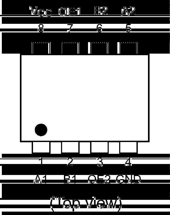
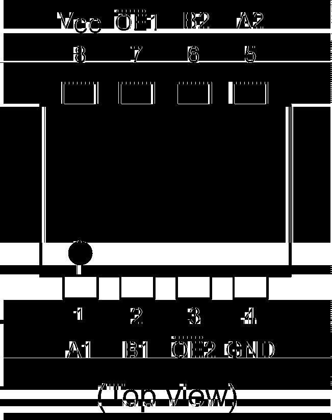
2 5. Pin Assignment TC7WB66CFK TC7WB67CFK TC7WB66CL8X TC7WB67CL8X 6. Marking TC7WB66CFK TC7WB67CFK TC7WB66CL8X TC7WB67CL8X 2
 H L Inputs OE (TC7WB67CFK/L8X) L H Function A port = B port Disconnect 9.")
 -0.5 to 7.0-0.5 to 7.0-0.5 to V CC +0.")
3 7. Block Diagram TC7WB66CFK,TC7WB66CL8X TC7WB67CFK,TC7WB67CL8X 8. Principle of Operation 8.1. Truth Table Inputs OE (TC7WB66CFK/L8X) H L Inputs OE (TC7WB67CFK/L8X) L H Function A port = B port Disconnect 9. Absolute Maximum Ratings (Note) Part Number Symbol Note Rating Unit Supply voltage Input voltage (OE, OE) Switch I/O voltage Clamp diode current Switch I/O current Power dissipation V CC /ground current Storage temperature TC7WB66CFK,TC7WB67CFK TC7WB66CL8X,TC7WB67CL8X V CC V IN V S I IK I S P D I CC /I GND T stg (Note 1) -0.5 to to to V CC ± to 150 Note: Exceeding any of the absolute maximum ratings, even briefly, lead to deterioration in IC performance or even destruction. Using continuously under heavy loads (e.g. the application of high temperature/current/voltage and the significant change in temperature, etc.) may cause this product to decrease in the reliability significantly even if the operating conditions (i.e. operating temperature/current/voltage, etc.) are within the absolute maximum ratings and the operating ranges. Please design the appropriate reliability upon reviewing the Toshiba Semiconductor Reliability Handbook ( Handling Precautions / Derating Concept and Methods ) and individual reliability data (i.e. reliability test report and estimated failure rate, etc). Note 1: Mounted on an FR4 board 10. Operating Ranges (Note) V ma mw ma Symbol Note Rating Unit Supply voltage Input voltage (OE, OE) Switch I/O voltage Operating temperature Input rise time Input fall time Note: V CC V IN V S T opr dt/dv dt/dv to to to V CC -40 to 85 0 to 10 0 to 10 The operating ranges must be maintained to ensure the normal operation of the device. Unused control inputs must be tied to either V CC or GND. V ns/v
4 11. Electrical TC7WB66CFK/L8X,TC7WB67CFK/L8X DC (Unless otherwise specified, T a = -40 to 85 ) High-level input voltage (OE, OE) Low-level input voltage (OE, OE) Input leakage current (OE, OE) Switch OFF-state leakage current ON-resistance Quiescent supply current Part Number TC7WB66- CFK/L8X TC7WB67- CFK/L8X Symbol V IH V IL I IN I SZ R ON I CC I CC Note (Note 1), (Note 2) Test Condition V IN = 0 to 5.5 V A, B = 0 to V CC, OE = GND A, B = 0 to V CC, OE = V CC V IS = 0 V, I IS = 30 ma V IS = 2.4 V, I IS = 30 ma V IS = 4.5 V, I IS = 30 ma V IS = 0 V, I IS = 24 ma V IS = 3.0 V, I IS = 24 ma V IS = 0 V, I IS = 8 ma V IS = 2.3 V, I IS = 8 ma V IS = 0 V, I IS = 4 ma V IS = 1.65 V, I IS = 4 ma V IN = V CC or GND, I OUT = 0 A V IN = V CC V V CC (V) 1.65 to to to to to to to Min 0.8 V CC 0.7 V CC Typ Max 0.2 V CC 0.3 V CC Note 1: All typical values are at T a = 25. Note 2: Measured by the voltage drop between A and B pins at the indicated current through the switch. On-resistance is determined by the lower of the voltages on the two (A or B) pins AC (Unless otherwise specified, T a = -40 to 85 ) ±1.0 ±10 ± Unit V µa Ω µa Symbol Note Test Condition V CC (V) Min Max Unit 3-state output enable time t PZL /t PZH See Fig , , Table ± ± ns 2.5 ± ± state output disable time t PLZ /t PHZ See Fig , , Table ± ± ± ±
 C IN V IN = 0 V 5.")

5 11.3. Capacitive (Note) (Unless otherwise specified, T a = 25 ) Part Number Symbol Note Test Condition V CC (V) Typ. Unit Input capacitance (OE, OE) C IN V IN = 0 V pf Switch terminal OFFcapacitance TC7WB66CFK/L8X TC7WB67CFK/L8X C I/O OE = GND, V I/O = 0 V OE = V CC, V I/O = 0 V Switch terminal ONcapacitance TC7WB66CFK/L8X TC7WB67CFK/L8X C I/O OE = V CC, V I/O = 0 V OE = GND, V I/O = 0 V Note: Parameter guaranteed by design. Fig AC Test Circuit Table Parameter for AC Test Circuit Parameter t PLZ, t PZL t PHZ, t PZH Switch 2 V CC GND Fig AC Waveform t PLZ, t PHZ, t PZL, t PZH 5
 of the input.")
6 12. Rise and Fall Time (t r /t f ) The t r(out) and t f(out) values of the output signals are affected by the CR time constant of the input, which consists of the switch terminal capacitance (C I/O ) and the on-resistance (R ON ) of the input. In practice, the t r(out) and t f(out) values are also affected by the circuit's capacitance and resistance components other than the capacitance of TC7WB66CFK/L8X, TC7WB67CFK/L8X The t r /t f(out) values can be approximated as follows. (Figure 12.1, Table 12.1 shows the test circuit.) t r /t f(out) (approx) = - (C I/O + C L ) (R DRIVE + R ON ) ln (((V OH - V OL ) - V M ) / (V OH - V OL )) Where, R DRIVE is the output impedance of the previous-stage circuit. Calculation example: t r(out) (approx) = - ( ) E - 12 ( ) ln (((4.5-0) ) / (4.5-0)) = 2.1 ns Calculation conditions: V CC = 4.5 V, C L = 15 pf, R DRIVE = 120 Ω (output impedance of the previous IC), V M = 2.25 V (V CC /2) Output of the previous IC = digital (i.e., high-level voltage = V CC, low-level voltage = GND) Fig Calculation Circuit Table 12.1 Calculation Circuit V CC = 5.0 ± 0.5 V V CC = 3.3 ± 0.3 V V CC = 2.5 ± 0.2 V V CC = 1.8 ± 0.15 V V M V CC /2 V CC /2 V CC /2 V CC /2 6

7 13. Curves (Note) Fig R ON - V IS Note: The above characteristics curves are presented for reference only and not guaranteed by production test, unless otherwise noted. 7
 TOSHIBA: SSOP8-P-0.")
8 Package Dimensions Unit: mm TC7WB66CFK,TC7WB67CFK Weight: 0.01 g (typ.) TOSHIBA: SSOP8-P-0.50S Nickname: US8 Package Name(s) 8
 Package Name(s) TOSHIBA: P-UFLGA8-0202-0.")
9 Package Dimensions Unit: mm TC7WB66CL8X,TC7WB67CL8X Weight: g (typ.) Package Name(s) TOSHIBA: P-UFLGA Nickname: MP8 9
10 RESTRICTIONS ON PRODUCT USE Toshiba Corporation, and its subsidiaries and affiliates (collectively "TOSHIBA"), reserve the right to make changes to the information in this document, and related hardware, software and systems (collectively "Product") without notice. This document and any information herein may not be reproduced without prior written permission from TOSHIBA. Even with TOSHIBA's written permission, reproduction is permissible only if reproduction is without alteration/omission. Though TOSHIBA works continually to improve Product's quality and reliability, Product can malfunction or fail. Customers are responsible for complying with safety standards and for providing adequate designs and safeguards for their hardware, software and systems which minimize risk and avoid situations in which a malfunction or failure of Product could cause loss of human life, bodily injury or damage to property, including data loss or corruption. Before customers use the Product, create designs including the Product, or incorporate the Product into their own applications, customers must also refer to and comply with (a) the latest versions of all relevant TOSHIBA information, including without limitation, this document, the specifications, the data sheets and application notes for Product and the precautions and conditions set forth in the "TOSHIBA Semiconductor Reliability Handbook" and (b) the instructions for the application with which the Product will be used with or for. Customers are solely responsible for all aspects of their own product design or applications, including but not limited to (a) determining the appropriateness of the use of this Product in such design or applications; (b) evaluating and determining the applicability of any information contained in this document, or in charts, diagrams, programs, algorithms, sample application circuits, or any other referenced documents; and (c) validating all operating parameters for such designs and applications. TOSHIBA ASSUMES NO LIABILITY FOR CUSTOMERS' PRODUCT DESIGN OR APPLICATIONS. PRODUCT IS NEITHER INTENDED NOR WARRANTED FOR USE IN EQUIPMENTS OR SYSTEMS THAT REQUIRE EXTRAORDINARILY HIGH LEVELS OF QUALITY AND/OR RELIABILITY, AND/OR A MALFUNCTION OR FAILURE OF WHICH MAY CAUSE LOSS OF HUMAN LIFE, BODILY INJURY, SERIOUS PROPERTY DAMAGE AND/OR SERIOUS PUBLIC IMPACT ("UNINTENDED USE"). Except for specific applications as expressly stated in this document, Unintended Use includes, without limitation, equipment used in nuclear facilities, equipment used in the aerospace industry, medical equipment, equipment used for automobiles, trains, ships and other transportation, traffic signaling equipment, equipment used to control combustions or explosions, safety devices, elevators and escalators, devices related to electric power, and equipment used in finance-related fields. IF YOU USE PRODUCT FOR UNINTENDED USE, TOSHIBA ASSUMES NO LIABILITY FOR PRODUCT. For details, please contact your TOSHIBA sales representative. Do not disassemble, analyze, reverse-engineer, alter, modify, translate or copy Product, whether in whole or in part. Product shall not be used for or incorporated into any products or systems whose manufacture, use, or sale is prohibited under any applicable laws or regulations. The information contained herein is presented only as guidance for Product use. No responsibility is assumed by TOSHIBA for any infringement of patents or any other intellectual property rights of third parties that may result from the use of Product. No license to any intellectual property right is granted by this document, whether express or implied, by estoppel or otherwise. ABSENT A WRITTEN SIGNED AGREEMENT, EXCEPT AS PROVIDED IN THE RELEVANT TERMS AND CONDITIONS OF SALE FOR PRODUCT, AND TO THE MAXIMUM EXTENT ALLOWABLE BY LAW, TOSHIBA (1) ASSUMES NO LIABILITY WHATSOEVER, INCLUDING WITHOUT LIMITATION, INDIRECT, CONSEQUENTIAL, SPECIAL, OR INCIDENTAL DAMAGES OR LOSS, INCLUDING WITHOUT LIMITATION, LOSS OF PROFITS, LOSS OF OPPORTUNITIES, BUSINESS INTERRUPTION AND LOSS OF DATA, AND (2) DISCLAIMS ANY AND ALL EXPRESS OR IMPLIED WARRANTIES AND CONDITIONS RELATED TO SALE, USE OF PRODUCT, OR INFORMATION, INCLUDING WARRANTIES OR CONDITIONS OF MERCHANTABILITY, FITNESS FOR A PARTICULAR PURPOSE, ACCURACY OF INFORMATION, OR NONINFRINGEMENT. Do not use or otherwise make available Product or related software or technology for any military purposes, including without limitation, for the design, development, use, stockpiling or manufacturing of nuclear, chemical, or biological weapons or missile technology products (mass destruction weapons). Product and related software and technology may be controlled under the applicable export laws and regulations including, without limitation, the Japanese Foreign Exchange and Foreign Trade Law and the U.S. Export Administration Regulations. Export and re-export of Product or related software or technology are strictly prohibited except in compliance with all applicable export laws and regulations. Please contact your TOSHIBA sales representative for details as to environmental matters such as the RoHS compatibility of Product. Please use Product in compliance with all applicable laws and regulations that regulate the inclusion or use of controlled substances, including without limitation, the EU RoHS Directive. TOSHIBA ASSUMES NO LIABILITY FOR DAMAGES OR LOSSES OCCURRING AS A RESULT OF NONCOMPLIANCE WITH APPLICABLE LAWS AND REGULATIONS. 10
TC4028BP, TC4028BF TC4028BP/BF. TC4028B BCD-to-Decimal Decoder. Pin Assignment TOSHIBA CMOS Digital Integrated Circuit Silicon Monolithic
 TOSHIBA CMOS Digital Integrated Circuit Silicon Monolithic TC4028BP, TC4028BF TC4028B BCD-to-Decimal Decoder TC4028B is a BCD-to-DECIMAL decoder which converts BCD signal into DECIMAL signal. Of ten outputs
TC74HC155AP, TC74HC155AF
 TOSHIBA CMOS Digital Integrated Circuit Silicon Monolithic TC74HC155AP, TC74HC155AF Dual 2-to-4 Line Decoder 3-to-8 Line Decoder TC74HC155AP/AF The TC74HC155A is a high speed CMOS DUAL 2-to-4 LINE DECODER
TC74VCX14FT, TC74VCX14FK
 TOSHIBA CMOS Digital Integrated Circuit Silicon Monolithic TC74CX14FT, TC74CX14FK Low-oltage Hex Schmitt Inverter with 3.6- Tolerant Inputs and Outputs TC74CX14FT/FK The TC74CX14FT/FK is a high-performance
TC7SZ126F TC7SZ126F. 1. Functional Description. 2. Features. 3. Packaging Rev.3.0. Start of commercial production
 CMOS Digital Integrated Circuits TC7SZ126F Silicon Monolithic TC7SZ126F 1. Functional Description Bus Buffer with 3-State Output 2. Features (1) AEC-Q100 (Rev. H) (Note 1) (2) Wide operating temperature
TOSHIBA Field Effect Transistor Silicon N Channel MOS Type SSM6N15FE
 SSMNFE TOSHIBA Field Effect Transistor Silicon N Channel MOS Type SSMNFE High Speed Switching Applications Analog Switching Applications Unit: mm Small package Low ON resistance : R on =. Ω (max) (@V GS
TOSHIBA Field Effect Transistor Silicon N Channel MOS Type SSM6N44FE. DC I D 100 ma Pulse I DP 200
 SSMNFE TOSHIBA Field Effect Transistor Silicon N Channel MOS Type SSMNFE High Speed Switching Applications Analog Switching Applications.±. Unit: mm Compact package suitable for high-density mounting Low
TOSHIBA Field-Effect Transistor Silicon N Channel MOS Type (U-MOSⅣ) SSM6N7002BFU. DC I D 200 ma Pulse I DP 800
 SSM6N7002BFU. DC I D 200 ma Pulse I DP 800") TOSHIBA Field-Effect Transistor Silicon N Channel MOS Type (U-MOSⅣ) SSM6N7BFU High-Speed Switching Applications Analog Switch Applications Small package Low ON-resistance : R DS(ON) =. Ω (max) (@V GS =.
TOSHIBA Field-Effect Transistor Silicon N Channel MOS Type (U-MOSⅣ) SSM6N7BFU High-Speed Switching Applications Analog Switch Applications Small package Low ON-resistance : R DS(ON) =. Ω (max) (@V GS =.
TOSHIBA Field Effect Transistor Silicon N Channel MOS Type SSM6N37FU
 TOSHIBA Field Effect Transistor Silicon N Channel MOS Type SSM6N7FU High Speed Switching Applications Analog Switch Applications Unit: mm.v drive Low ON-resistance R DS(ON) =.6 Ω (max) (@V GS =. V) R DS(ON)
Derating of the MOSFET Safe Operating Area Outline:
 Outline: This document discusses temperature derating of the MOSFET safe operating area. Table of Contents Outline:... 1 Table of Contents... 2 1. Introduction... 3 2. What is the safe operating area?...
TC7WP3125FK, TC7WP3125FC
 TOSHIBA Digital Integrated Circuit Silicon Monolithic TC7WP3125FK, TC7WP3125FC Low oltage/low Power 2-Bit Dual Supply Bus Buffer TC7WP3125FK/FC The TC7WP3125 is a dual supply, advanced high-speed CMOS
TOSHIBA Digital Integrated Circuit Silicon Monolithic TC7SP3125CFC
 TOSHIBA Digital Integrated Circuit Silicon Monolithic TC7SP3125CFC Low oltage/low Power 1-Bit Dual Supply Bus Buffer The TC7SP3125 is an advanced high-speed CMOS 1-bit dual supply voltage interface bus
TOSHIBA Field-Effect Transistor Silicon N / P Channel MOS Type SSM6L35FE
 SSM6L3FE TOSHIBA Field-Effect Transistor Silicon N / P Channel MOS Type SSM6L3FE High-Speed Switching Applications Analog Switch Applications.6±. Unit: mm N-ch:.2-V drive.2±. P-ch:.2-V drive N-ch, P-ch,
TOSHIBA CMOS Digital Integrated Circuit Silicon Monolithic TC74VCX164245FT
 16-Bit Dual Supply Bus Transceiver TOSHIBA CMOS Digital Integrated Circuit Silicon Monolithic TC74CX164245FT TC74CX164245FT The TC74CX164245FT is a dual supply, advanced high-speed CMOS 16-bit bus transceiver
TC74HC697AP, TC74HC697AF
 TOSHIBA CMOS Digital Integrated Circuit Silicon Monolithic TC74HC697AP, TC74HC697AF TC74HC697AP/AF Synchronous Presettable 4-Bit Binary Up/Down Counter with Output Register (multiplexed 3-state outputs)
TPCP8404 TPCP8404. Portable Equipment Applications Motor Drive Applications. Absolute Maximum Ratings (Ta = 25 C) Circuit Configuration
 Circuit Configuration") TOSHIBA Field Effect Transistor Silicon P, N Channel MOS Type (U-MOⅤ/U-MOSⅣ) TPCP8 Portable Equipment Applications Motor Drive Applications Low drain-source ON-resistance : P Channel R DS (ON) = 38 mω(typ.)
TOSHIBA Field Effect Transistor Silicon P, N Channel MOS Type (U-MOⅤ/U-MOSⅣ) TPCP8 Portable Equipment Applications Motor Drive Applications Low drain-source ON-resistance : P Channel R DS (ON) = 38 mω(typ.)
TOSHIBA CMOS Digital Integrated Circuit Silicon Monolithic TC7SG02FU IN A GND
 TOSHIBA CMOS Digital Integrated Circuit Silicon Monolithic TC7SG02FU 2 Input NOR Gate Features High-level output current: I OH /I OL = ±8 ma (min) at = 3.0 High-speed operation: t pd = 2.4 ns (typ.) at
TC7SZ08FU TC7SZ08FU. 1. Functional Description. 2. Features. 3. Packaging Rev Toshiba Corporation
 CMOS Digital Integrated Circuits TC7SZ08FU Silicon Monolithic TC7SZ08FU 1. Functional Description 2-Input AND Gate 2. Features (1) AEC-Q100 (Rev. ) (Note 1) (2) Wide operating temperature range: T opr
TC74LCX244F,TC74LCX244FW,TC74LCX244FT,TC74LCX244FK
 TOSHIBA CMOS Digital Integrated Circuit Silicon Monolithic TC74LCX244F/FW/FT/FK TC74LCX244F,TC74LCX244FW,TC74LCX244FT,TC74LCX244FK Low-Voltage Octal Bus Buffer with 5-V Tolerant Inputs and Outputs The
TOSHIBA Field Effect Transistor Silicon N Channel MOS Type (π-mosiii) 2SK2613
 2SK2613") SK6 TOSHIBA Field Effect Transistor Silicon N Channel MOS Type (π-mosiii) SK6 Switching Regulator Applications, DC-DC Converter and Motor Drive Applications Unit: mm Low drain-source ON-resistance: R DS
SK6 TOSHIBA Field Effect Transistor Silicon N Channel MOS Type (π-mosiii) SK6 Switching Regulator Applications, DC-DC Converter and Motor Drive Applications Unit: mm Low drain-source ON-resistance: R DS
TC74LCX08F,TC74LCX08FN,TC74LCX08FT,TC74LCX08FK
 TOSHIBA CMOS Digital Integrated Circuit Silicon Monolithic TC74LCX08F/FN/FT/FK TC74LCX08F,TC74LCX08FN,TC74LCX08FT,TC74LCX08FK Low-Voltage Quad 2-Input AND Gate with 5-V Tolerant Inputs and Outputs The
Rating Q1 Q (Note 4a)
") TPCA Q:TOSHIBA FIELD EFFECT TRANSISTOR SILICON N CHANNEL MOS TYPE(U-MOSⅢ) Q:TOSHIBA INCLUDES SCHOTTKY BARRIER DIODE FIELD EFFECT TRANSISTOR SILICON N CHANNEL MOS TYPE(U-MOSⅢ) TPCA DC-DC CONVERTER Notebook
TPCA Q:TOSHIBA FIELD EFFECT TRANSISTOR SILICON N CHANNEL MOS TYPE(U-MOSⅢ) Q:TOSHIBA INCLUDES SCHOTTKY BARRIER DIODE FIELD EFFECT TRANSISTOR SILICON N CHANNEL MOS TYPE(U-MOSⅢ) TPCA DC-DC CONVERTER Notebook
TOSHIBA Field Effect Transistor Silicon P/N-Channel MOS Type (P-Channel/N-Channel Ultra-High-Speed U-MOSIII) TPC8406-H. Rating P-Channel N-Channel
 TPC8406-H. Rating P-Channel N-Channel") TPC86-H TOSHIBA Field Effect Transistor Silicon P/N-Channel MOS Type (P-Channel/N-Channel Ultra-High-Speed U-MOSIII) TPC86-H High Efficiency DC/DC Converter Applications Notebook PC Applications Portable
TPC86-H TOSHIBA Field Effect Transistor Silicon P/N-Channel MOS Type (P-Channel/N-Channel Ultra-High-Speed U-MOSIII) TPC86-H High Efficiency DC/DC Converter Applications Notebook PC Applications Portable
TC74VHCT573AF,TC74VHCT573AFW,TC74VHCT573AFT
 TOSHIBA CMOS igital Integrated Circuit Silicon Monolithic TC74HCT573AF/AFW/AFT TC74HCT573AF,TC74HCT573AFW,TC74HCT573AFT Octal -Type Latch with 3-State Output The TC74HCT573A is an advanced high speed CMOS
TC74HC373AP,TC74HC373AF,TC74HC373AFW
 TOSHIBA CMOS Digital Integrated Circuit Silicon Monolithic TC74HC373AP/AF/AFW TC74HC373AP,TC74HC373AF,TC74HC373AFW Octal D-Type Latch with 3-State Output The TC74HC373A is a high speed CMOS OCTAL LATCH
TC4013BP,TC4013BF,TC4013BFN
 TOSHIBA CMOS Digital Integrated Circuit Silicon Monolithic TC4013BP,TC4013BF,TC4013BFN TC4013B Dual D-Type Flip Flop TC4013B contains two independent circuits of D type flip-flop. The input level applied
TC4066BP,TC4066BF,TC4066BFN,TC4066BFT
 TOSHIBA MOS Digital Integrated ircuit Silicon Monolithic T466BP/BF/BFN/BFT T466BP,T466BF,T466BFN,T466BFT T466B Quad Bilateral Switch T466B contains four independent circuits of bidirectional switches.
Discrete Semiconductor Devices
 Discrete Semiconductor Devices Hints and Tips for Thermal Design Part 2 Outline: This document provides hints and tips based on simulation results to help you reduce the chip temperature of discrete semiconductor
TOSHIBA Field Effect Transistor Silicon N Channel MOS Type SSM3K02F
 TOSHIBA Field Effect Transistor Silicon N Channel MOS Type SSM3K02F High Speed Switching Applications Unit: mm Small package Low on resistance : R on = 200 mω (max) (V GS = 4 V) : R on = 250 mω (max) (V
TC74HC148AP,TC74HC148AF
 TOSHIBA CMOS Digital Integrated Circuit Silicon Monolithic TC74HC148AP,TC74HC148AF 8-to-3 Line Priority Encoder The TC74HC148A is a high speed CMOS 8-to-3 LINE ENCODER fabricated with silicon gate C2MOS
74VHCT540AFT,74VHCT541AFT
 CMOS Digital Integrated Circuits Silicon Monolithic 1. Functional Description Octal Bus Buffer : INERTED, 3-STATE OUTPUTS : NON-INERTED, 3-STATE OUTPUTS 2. General The and are advanced high speed CMOS
TC74HC4051AP,TC74HC4051AF,TC74HC4051AFT TC74HC4052AP,TC74HC4052AF,TC74HC4052AFT TC74HC4053AP,TC74HC4053AF,TC74HC4053AFN,TC74HC4053AFT
 T4H40,40P/F/FT,40P/F/FN/FT TOSHI MOS Digital Integrated ircuit Silicon Monolithic T4H40P,T4H40F,T4H40FT T4H40P,T4H40F,T4H40FT T4H40P,T4H40F,T4H40FN,T4H40FT T4H40P/F/FT 8-hannel nalog Multiplexer/Demulitiplexer
TC74HC7292AP,TC74HC7292AF
 TOSHIBA CMOS Digital Integrated Circuit Silicon Monolithic TC74HC7292AP,TC74HC7292AF Programmable Divider/Timer The TC74HC7292A is a high speed CMOS PROGRAMMABLE DIVIDER/TIMER fabricated with silicon gate
TC74VHC573F,TC74VHC573FW,TC74VHC573FT,TC74VHC573FK
 TOSHIBA CMOS igital Integrated Circuit Silicon Monolithic TC74VHC573F/FW/FT/FK TC74VHC573F,TC74VHC573FW,TC74VHC573FT,TC74VHC573FK Octal -Type Latch with 3-State Output The TC74VHC573 is an advanced high
Product Guide Microwave Semiconductors
 Product Guide 13 Microwave Semiconductors C O N T E N T S Output Power vs. Frequency Map GaAs MMICs L and S-band Partially Matched Power GaAs FETs... 3 C-band Internally Matched Power GaAs FETs/GaN HEMTs...
TC74VHC574F,TC74VHC574FW,TC74VHC574FT,TC74VHC574FK
 TOSHIBA CMOS igital Integrated Circuit Silicon Monolithic TC74VHC574F/FW/FT/FK TC74VHC574F,TC74VHC574FW,TC74VHC574FT,TC74VHC574FK Octal -Type Flip Flop with 3-State Output The TC74VHC574 is advanced high
TC74HC74AP,TC74HC74AF,TC74HC74AFN
 TOSHIBA CMOS Digital Integrated Circuit Silicon Monolithic TC74HC74AP/AF/AFN TC74HC74AP,TC74HC74AF,TC74HC74AFN Dual D-Type Flip Flop Preset and Clear The TC74HC74A is a high speed CMOS D FLIP FLOP fabricated
TOSHIBA Field Effect Transistor Silicon P Channel MOS Type SSM3J16TE. DC I D 100 ma Pulse I DP 200
 High Speed Switching Applications Analog Switch Applications TOSHIBA Field Effect Transistor Silicon P Channel MOS Type SSMJ6TE Small package Low on-resistance : R on = 8 Ω (max) (@V GS = 4 V) : R on =
TOSHIBA Field-Effect Transistor Silicon P-Channel MOS Type SSM3J117TU. Characteristic Symbol Test Condition Min Typ. Max Unit
 TOSHIBA Field-Effect Transistor Silicon P-Channel MOS Type SSMJ7TU High-Speed Switching Applications 4 V drive Low ON-resistance: R on = 225 mω (max) (@V GS = ) R on = 7 mω (max) (@V GS = V) Absolute Maximum
TOSHIBA Field Effect Transistor Silicon N Channel MOS Type SSM3K17FU
 SSMK7FU TOSHIBA Field Effect Transistor Silicon N Channel MOS Type SSMK7FU High Speed Switching Applications Analog Switch Applications Unit: mm Suitable for high-density mounting due to compact package
TOSHIBA Photo-IC Silicon Epitaxial Planar TPS856
 TOSHIBA Photo-IC Silicon Epitaxial Planar TPS856 Mobile Phones Notebook PCs, PDAs Video cameras, Digital Still Cameras Other Equipment Requiring Luminosity Adjustment The TPS856 is an ultra-compact surface-mount
TC74VHC164F,TC74VHC164FN,TC74VHC164FT,TC74VHC164FK
 TOSHIBA CMOS igital Integrated Circuit Silicon Monolithic TC74VHC164F/FN/FT/FK TC74VHC164F,TC74VHC164FN,TC74VHC164FT,TC74VHC164FK 8-Bit Shift egister (S-IN, P-OUT) The TC74VHC164 is an advanced high speed
TC4511BP,TC4511BF TC4511BP/BF. TC4511B BCD-to-Seven Segment Latch/Decoder/Driver. Pin Assignment. Display
 TC411BP/BF TOSHIBA CMOS Digital Integrated Circuit Silicon Monolithic TC411BP,TC411BF TC411B BCD-to-Seven Segment Latch/Decoder/Driver TC411B is decoder which converts the input of BCD code into the 7
TOSHIBA Field Effect Transistor Silicon N Channel MOS Type (U-MOSIII) TPC6004
 TPC6004") TPC TOSHIBA Field Effect Transistor Silicon N Channel MOS Type (U-MOSIII) TPC Notebook PC Applications Portable Equipment Applications Unit: mm Low drain-source ON resistance: R DS (ON) = 9 mω (typ.) High
TPC TOSHIBA Field Effect Transistor Silicon N Channel MOS Type (U-MOSIII) TPC Notebook PC Applications Portable Equipment Applications Unit: mm Low drain-source ON resistance: R DS (ON) = 9 mω (typ.) High
TOSHIBA Photo IC Silicon Epitaxial Planar TPS859
 TOSHIBA Photo IC Silicon Epitaxial Planar Flat Panel Displays Mobile Phones Notebook PCs, PDAs Video cameras, Digital Still Cameras Other Equipment Requiring Luminosity Adjustment The is an ultra-compact
TOSHIBA Field Effect Transistor Silicon N Channel MOS Type (U-MOS IV) TPC8026
 TPC8026") TPC26 TOSHIBA Field Effect Transistor Silicon N Channel MOS Type (U-MOS IV) TPC26 Lithium Ion Battery Applications Portable Equipment Applications Notebook PC Applications Unit: mm Small footprint due
TPC26 TOSHIBA Field Effect Transistor Silicon N Channel MOS Type (U-MOS IV) TPC26 Lithium Ion Battery Applications Portable Equipment Applications Notebook PC Applications Unit: mm Small footprint due
2-input AND gate with open-drain output. The 74AHC1G09 is a high-speed Si-gate CMOS device.
 74HC1G09 Rev. 02 18 December 2007 Product data sheet 1. General description 2. Features 3. Ordering information The 74HC1G09 is a high-speed Si-gate CMOS device. The 74HC1G09 provides the 2-input ND function
TOSHIBA Field Effect Transistor Silicon P Channel MOS Type (U-MOSⅣ) TPCA8103
 TPCA8103") TOSHIBA Field Effect Transistor Silicon P Channel MOS Type (U-MOSⅣ) TPCA83 TPCA83 Lithium Ion Battery Applications Notebook PC Applications Portable Equipment Applications.±..27 8.4±. Unit: mm. M A Small
TOSHIBA Field Effect Transistor Silicon P Channel MOS Type (U-MOSⅣ) TPCA83 TPCA83 Lithium Ion Battery Applications Notebook PC Applications Portable Equipment Applications.±..27 8.4±. Unit: mm. M A Small
TOSHIBA Field Effect Transistor Silicon N-Channel MOS Type (Ultra-High-speed U-MOSIII) TPCA8011-H
 TPCA8011-H") TPCA-H TOSHIBA Field Effect Transistor Silicon N-Channel MOS Type (Ultra-High-speed U-MOSIII) TPCA-H High Efficiency DC/DC Converter Applications Notebook PC Applications Portable-Equipment Applications.±..7.±..
TPCA-H TOSHIBA Field Effect Transistor Silicon N-Channel MOS Type (Ultra-High-speed U-MOSIII) TPCA-H High Efficiency DC/DC Converter Applications Notebook PC Applications Portable-Equipment Applications.±..7.±..
74HC253; 74HCT253. Dual 4-input multiplexer; 3-state
 Rev. 6 1 February 2016 Product data sheet 1. General description The is a dual 4-bit multiplexer, each with four binary inputs (ni0 to ni3), an output enable input (noe) and shared select inputs (S0 and
TOSHIBA Field Effect Transistor Silicon N Channel MOS Type (π MOSV) 2SK3497
 2SK3497") TOSHIBA Field Effect Transistor Silicon N Channel MOS Type (π MOSV) High Power Amplifier Application Unit: mm High breakdown voltage: V DSS = 8 V Complementary to SJ68.. MAX. 5.9 MAX. Ф. ±... 9..5. ±..
TOSHIBA Field Effect Transistor Silicon N Channel MOS Type (π MOSV) High Power Amplifier Application Unit: mm High breakdown voltage: V DSS = 8 V Complementary to SJ68.. MAX. 5.9 MAX. Ф. ±... 9..5. ±..
TA7262P,TA7262P(LB),TA7262F
,TA7262F") TOSHIBA BIPOLAR LINEAR INTEGRATED CIRCUIT SILICON MONOLITHIC TA7262P,TA7262P(LB),TA7262F DC MOTOR DRIVER (3 PHASE Bi DIRECTIONAL) The TA7262P / P (LB) / F are 3 Phase Bi Directional supply voltage control
TOSHIBA BIPOLAR LINEAR INTEGRATED CIRCUIT SILICON MONOLITHIC TA7262P,TA7262P(LB),TA7262F DC MOTOR DRIVER (3 PHASE Bi DIRECTIONAL) The TA7262P / P (LB) / F are 3 Phase Bi Directional supply voltage control
74HC366; 74HCT366. Hex buffer/line driver; 3-state; inverting
 Rev. 5 2 February 2016 Product data sheet 1. General description The is a hex inverting buffer/line driver with 3-state outputs controlled by the output enable inputs (OEn). A HIGH on OEn causes the outputs
Octal buffer/line driver; 3-state
 Rev. 4 1 March 2016 Product data sheet 1. General description The is a low-voltage Si-gate CMOS device and is pin and function compatible with 74HC244 and 74HCT244. The is an octal non-inverting buffer/line
74HC368; 74HCT368. Hex buffer/line driver; 3-state; inverting
 Rev. 3 9 August 2016 Product data sheet 1. General description 2. Features and benefits 3. Ordering information The is a hex inverting buffer/line driver with 3-state outputs controlled by the output enable
74LVC1G125-Q100. Bus buffer/line driver; 3-state
 Rev. 2 8 December 2016 Product data sheet 1. General description The provides one non-inverting buffer/line driver with 3-state output. The 3-state output is controlled by the output enable input (OE).
74HC365; 74HCT365. Hex buffer/line driver; 3-state
 Rev. 4 27 January 2016 Product data sheet 1. General description 2. Features and benefits The is a hex buffer/line driver with 3-state outputs controlled by the output enable inputs (OEn). A HIGH on OEn
74AVC16374-Q General description. 2. Features and benefits. 16-bit edge triggered D-type flip-flop; 3.6 V tolerant; 3-state
 Rev. 2 16 March 2015 Product data sheet 1. General description The is a 16-bit edge triggered flip-flop featuring separate D-type inputs for each flip-flop and 3-state outputs for bus-oriented applications.
74HC541; 74HCT541. Octal buffer/line driver; 3-state
 Rev. 4 3 March 2016 Product data sheet 1. General description 2. Features and benefits The is an octal non-inverting buffer/line driver with 3-state outputs. The device features two output enables (OE1
74HC2G16; 74HCT2G16. The 74HC2G16; 74HCT2G16 is a high-speed Si-gate CMOS device. The 74HC2G16; 74HCT2G16 provides two buffers.
 Rev. 1 2 November 2015 Product data sheet 1. General description The is a high-speed Si-gate CMOS device. The provides two buffers. 2. Features and benefits 3. Ordering information Wide supply voltage
TOSHIBA Field Effect Transistor Silicon N-Channel MOS Type (U-MOSⅤ-H) TPC8037-H
 TPC8037-H") TOSHIBA Field Effect Transistor Silicon N-Channel MOS Type (U-MOSⅤ-H) TPC7-H TPC7-H High-Efficiency DC-DC Converter Applications Notebook PC Applications Portable Equipment Applications Unit: mm Small
TOSHIBA Field Effect Transistor Silicon N-Channel MOS Type (U-MOSⅤ-H) TPC7-H TPC7-H High-Efficiency DC-DC Converter Applications Notebook PC Applications Portable Equipment Applications Unit: mm Small
TOSHIBA Field Effect Transistor Silicon N-Channel MOS Type (π-mos VI) 2SK4108. JEDEC Repetitive avalanche energy (Note 3) E AR 15 mj
 2SK4108. JEDEC Repetitive avalanche energy (Note 3) E AR 15 mj") SK TOSHIBA Field Effect Transistor Silicon N-Channel MOS Type (π-mos VI) SK Switching Regulator Applications Unit: mm Low drain source ON resistance : R DS (ON) =. Ω (typ.) High forward transfer admittance
SK TOSHIBA Field Effect Transistor Silicon N-Channel MOS Type (π-mos VI) SK Switching Regulator Applications Unit: mm Low drain source ON resistance : R DS (ON) =. Ω (typ.) High forward transfer admittance
TOSHIBA Field Effect Transistor Silicon N Channel MOS Type (DTMOS ) TK15J60U
 TK15J60U") TOSHIBA Field Effect Transistor Silicon N Channel MOS Type (DTMOS ) Switching Regulator Applications Unit: mm Low drain-source ON-resistance: R DS (ON) =. (typ.) High forward transfer admittance: Y fs
TOSHIBA Field Effect Transistor Silicon N Channel MOS Type (DTMOS ) Switching Regulator Applications Unit: mm Low drain-source ON-resistance: R DS (ON) =. (typ.) High forward transfer admittance: Y fs
The 74LV08 provides a quad 2-input AND function.
 Rev. 4 8 December 2015 Product data sheet 1. General description The is a low-voltage Si-gate CMOS device that is pin and function compatible with 74HC08 and 74HCT08. The provides a quad 2-input AND function.
TOSHIBA Field Effect Transistor Silicon N Channel MOS Type (π-mosvi) 2SK3667
 2SK3667") SK7 TOSHIBA Field Effect Transistor Silicon N Channel MOS Type (π-mosvi) SK7 Switching Regulator Applications Unit: mm Low drain-source ON resistance: R DS (ON) =.7Ω (typ.) High forward transfer admittance:
SK7 TOSHIBA Field Effect Transistor Silicon N Channel MOS Type (π-mosvi) SK7 Switching Regulator Applications Unit: mm Low drain-source ON resistance: R DS (ON) =.7Ω (typ.) High forward transfer admittance:
74HC30; 74HCT General description. 2. Features and benefits. 3. Ordering information. 8-input NAND gate
 Rev. 7 2 December 2015 Product data sheet 1. General description 2. Features and benefits 3. Ordering information The is an. Inputs include clamp diodes. This enables the use of current limiting resistors
MM74HC251 8-Channel 3-STATE Multiplexer
 8-Channel 3-STATE Multiplexer General Description The MM74HC251 8-channel digital multiplexer with 3- STATE outputs utilizes advanced silicon-gate CMOS technology. Along with the high noise immunity and
TOSHIBA Field Effect Transistor Silicon N Channel MOS Type (U-MOS IV) TPC8028
 TPC8028") TPC TOSHIBA Field Effect Transistor Silicon N Channel MOS Type (U-MOS IV) TPC Lithium Ion Battery Applications Portable Equipment Applications Notebook PC Applications Unit: mm Small footprint due to small
TPC TOSHIBA Field Effect Transistor Silicon N Channel MOS Type (U-MOS IV) TPC Lithium Ion Battery Applications Portable Equipment Applications Notebook PC Applications Unit: mm Small footprint due to small
74HC126; 74HCT126. Quad buffer/line driver; 3-state
 Rev. 3 22 September 2014 Product data sheet 1. General description 2. Features and benefits 3. Ordering information The is a quad buffer/line driver with 3-state outputs controlled by the output enable
4-bit dual-supply buffer/level translator; 3-state
 Rev. 1 18 December 017 Product data sheet 1 General description Features and benefits The is a -bit, dual-supply level translating buffer with -state outputs. It features four data inputs (An and B), four
74ALVC bit dual supply translating transciever; 3-state. This device can be used as two 8-bit transceivers or one 16-bit transceiver.
 16-bit dual supply translating transciever; 3-state Rev. 02 1 June 2004 Product data sheet 1. General description 2. Features The is a high-performance, low-power, low-voltage, Si-gate CMOS device, superior
TOSHIBA Field Effect Transistor Silicon P-Channel MOS Type (U MOSIII) 2SJ668
 2SJ668") TOSHIBA Field Effect Transistor Silicon P-Channel MOS Type (U MOSIII) 2SJ668 Relay Drive, DC/DC Converter and Motor Drive Applications Unit: mm 4 V gate drive Low drain source ON-resistance: R DS (ON)
TOSHIBA Field Effect Transistor Silicon P-Channel MOS Type (U MOSIII) 2SJ668 Relay Drive, DC/DC Converter and Motor Drive Applications Unit: mm 4 V gate drive Low drain source ON-resistance: R DS (ON)
NLSV2T Bit Dual-Supply Inverting Level Translator
 2-Bit Dual-Supply Inverting Level Translator The NLSV2T240 is a 2 bit configurable dual supply voltage level translator. The input A n and output B n ports are designed to track two different power supply
74LVC1G18 1-of-2 non-inverting demultiplexer with 3-state deselected output Rev. 3 2 December 2016 Product data sheet 1. General description
 1-of-2 non-inverting demultiplexer with 3-state deselected output Rev. 3 2 December 2016 Product data sheet 1. General description The is a 1-of-2 non-inverting demultiplexer with a 3-state output. The
CD54/74AC153, CD54/74ACT153
 CD4/74AC13, CD4/74ACT13 Data sheet acquired from Harris Semiconductor SCHS237A September 1998 - Revised May 2000 Dual 4-Input Multiplexer Features Description [ /Title (CD74 AC13, CD74 ACT1 3) /Subject
TPCA8107-H 4± ± M A .0±.0± 0.15± ± ± ± ± ± 4.25±0.2 5±0. 3. Maximum Ratings (Ta 25 C)
") TOSHIBA Field Effect Transistor Silicon P-Channel MOS Type (Ultra-High-speed U-MOSIII) High Efficiency DC/DC Converter Applications Notebook PC Applications Portable Equipment Applications CCFL Inverter
TOSHIBA Field Effect Transistor Silicon P-Channel MOS Type (Ultra-High-speed U-MOSIII) High Efficiency DC/DC Converter Applications Notebook PC Applications Portable Equipment Applications CCFL Inverter
74VHC08; 74VHCT08. The 74VHC08; 74VHCT08 provide the quad 2-input AND function.
 Rev. 0 30 June 2009 Product data sheet. General description 2. Features 3. Ordering information The are high-speed Si-gate CMOS devices and are pin compatible with Low-power Schottky TTL (LSTTL). They
Bus buffer/line driver; 3-state
 Rev. 12 2 December 2016 Product data sheet 1. General description The provides one non-inverting buffer/line driver with 3-state output. The 3-state output is controlled by the output enable input (OE).
The 74AUP2G34 provides two low-power, low-voltage buffers.
 Rev. 6 17 September 2015 Product data sheet 1. General description The provides two low-power, low-voltage buffers. Schmitt trigger action at all inputs makes the circuit tolerant to slower input rise
74LVC374 Octal D-type flip-flop; positive edge-trigger (3-State) INTEGRATED CIRCUITS
 INTEGRATED CIRCUITS") INTEGRATE CIRCUITS Octal -type flip-flop; positive edge-trigger (3-State) Supersedes data of February 1996 IC24 ata Handbook 1997 Mar 12 FEATURES Wide supply voltage range of 1.2V to 3.6V In accordance
INTEGRATE CIRCUITS Octal -type flip-flop; positive edge-trigger (3-State) Supersedes data of February 1996 IC24 ata Handbook 1997 Mar 12 FEATURES Wide supply voltage range of 1.2V to 3.6V In accordance
Quad bus transceiver; 3-state. The output enable inputs (OEA and OEB) can be used to isolate the buses.
 can be used to isolate the buses.") Rev. 03 12 November 2004 Product data sheet 1. General description 2. Features The is a high-speed Si-gate CMOS device and is pin compatible with low power Schottky TTL (LSTTL). The is specified in compliance
Rev. 03 12 November 2004 Product data sheet 1. General description 2. Features The is a high-speed Si-gate CMOS device and is pin compatible with low power Schottky TTL (LSTTL). The is specified in compliance
74AVC General description. 2 Features and benefits. 1-to-4 fan-out buffer
 Rev. 1 23 April 2018 Product data sheet 1 General description 2 Features and benefits The is a suitable for use in clock distribution. It has a data input (A), four data outputs (Yn) and an output enable
NTE74HC173 Integrated Circuit TTL High Speed CMOS, 4 Bit D Type Flip Flop with 3 State Outputs
 NTE74HC173 Integrated Circuit TTL High Speed CMOS, 4 Bit D Type Flip Flop with 3 State Outputs Description: The NTE74HC173 is an high speed 3 State Quad D Type Flip Flop in a 16 Lead DIP type package that
Temperature range Name Description Version XC7SET32GW 40 C to +125 C TSSOP5 plastic thin shrink small outline package; 5 leads; body width 1.
 Rev. 01 3 September 2009 Product data sheet 1. General description 2. Features 3. Ordering information is a high-speed Si-gate CMOS device. It provides a 2-input OR function. Symmetrical output impedance
74HC General description. 2. Features. Octal D-type flip-flop; positive-edge trigger; 3-state; inverting
 Rev. 03 11 November 2004 Product data sheet 1. General description 2. Features The is a high-speed Si-gate CMOS device and is pin compatible with low-power Schottky TTL (LSTTL). The is specified in compliance
TOSHIBA Field Effect Transistor Silicon N Channel MOS Type (Ultra-High-Speed U-MOSIII) TPC8017-H
 TPC8017-H") TPC7-H TOSHIBA Field Effect Transistor Silicon N Channel MOS Type (Ultra-High-Speed U-MOSIII) TPC7-H High-Efficiency DC/DC Converter Applications Notebook PC Applications Portable-Equipment Applications
TPC7-H TOSHIBA Field Effect Transistor Silicon N Channel MOS Type (Ultra-High-Speed U-MOSIII) TPC7-H High-Efficiency DC/DC Converter Applications Notebook PC Applications Portable-Equipment Applications
8-bit binary counter with output register; 3-state
 Rev. 01 30 March 2005 Product data sheet 1. General description 2. Features 3. Quick reference data The is a high-speed Si-gate CMOS device and is pin compatible with Low power Schottky TTL (LSTTL). It
74HC280; 74HCT bit odd/even parity generator/checker
 Rev. 3 15 September 2016 Product data sheet 1. General description 2. Features and benefits 3. Ordering information The is a 9-bit parity generator or checker. Both even and odd parity outputs are available.
The 74AXP1G04 is a single inverting buffer.
 Rev. 1 25 August 2014 Product data sheet 1. General description The is a single inverting buffer. Schmitt-trigger action at all inputs makes the circuit tolerant of slower input rise and fall times. This
2-input EXCLUSIVE-OR gate
 Rev. 01 7 September 2009 Product data sheet 1. General description 2. Features 3. Ordering information is a high-speed Si-gate CMOS device. It provides a 2-input EXCLUSIVE-OR function. Symmetrical output
MM74HC573 3-STATE Octal D-Type Latch
 MM74HC573 3-STATE Octal D-Type Latch General Description The MM74HC573 high speed octal D-type latches utilize advanced silicon-gate P-well CMOS technology. They possess the high noise immunity and low
74HC2G125; 74HCT2G125
 Rev. 5 17 March 2014 Product data sheet 1. General description 2. Features and benefits The 74HC2G125; 74HC2G125 are dual buffer/line drivers with 3-state outputs controlled by the output enable inputs
74AVC20T245-Q General description. 2. Features and benefits
 20-bit dual supply translating transceiver with configurable voltage translation; 3-state Rev. 1 7 April 2016 Product data sheet 1. General description The is a 20 bit, dual supply transceiver that enables
Octal bus transceiver; 3-state
 Rev. 2 3 November 2016 Product data sheet 1. General description The is an 8-bit transceiver with 3-state outputs. The device features an output enable (OE) and send/receive (DIR) for direction control.
Low-power dual Schmitt trigger inverter
 Rev. 1 9 October 2014 Product data sheet 1. General description The is a dual inverter with Schmitt-trigger inputs. It transforms slowly changing input signals into sharply defined, jitter-free output
74ALVCH V/3.3 V 16-bit D-type transparent latch; 3-state
 Rev. 5 17 November 2011 Product data sheet 1. General description The is 16-bit D-type transparent latch featuring separate D-type inputs for each latch and 3-state outputs for bus oriented applications.
MM74HC244 Octal 3-STATE Buffer
 MM74HC244 Octal 3-STATE Buffer General Description The MM74HC244 is a non-inverting buffer and has two active low enables (1G and 2G); each enable independently controls 4 buffers. This device does not
MM74HC373 3-STATE Octal D-Type Latch
 3-STATE Octal D-Type Latch General Description The MM74HC373 high speed octal D-type latches utilize advanced silicon-gate CMOS technology. They possess the high noise immunity and low power consumption
74AHC2G126; 74AHCT2G126
 Rev. 04 27 pril 2009 Product data sheet 1. General description 2. Features 3. Ordering information The 74HC2G126 and 74HCT2G126 are high-speed Si-gate CMOS devices. They provide a dual non-inverting buffer/line
74AVC4T774PW. 4-bit dual supply translating transceiver; 3-state
 Rev. 1 25 September 2017 Product data sheet 1 General description 2 Features and benefits The is a 4-bit, dual supply transceiver that enables bidirectional level translation. It features eight 1-bit input-output
The 74LV08 provides a quad 2-input AND function.
 Quad 2-input ND gate Rev. 03 6 pril 2009 Product data sheet. General description 2. Features 3. Ordering information The is a low-voltage Si-gate CMOS device that is pin and function compatible with 74HC0