Drop Impact Reliability Test and Failure Analysis for Large Size High Density FOWLP Package on Package
|
|
|
- Winfred Chapman
- 5 years ago
- Views:
Transcription
1 2017 IEEE 67th Electronic Components and Technology Conference Drop Impact Reliability Test and Failure Analysis for Large Size High Density FOWLP Package on Package Zhaohui Chen, Faxing Che, Mian Zhi Ding, David Soon Wee Ho, Tai Chong Chai, Vempati Srinivasa Institute of Microelectronics, A*STAR (Agency for Science, Technology and Research), 2 Fusionnopolis Way, #08-02, Innovis, Singapore, chenz@ime.a-star.edu.sg Abstract Reliability of the 20 mm 20 mm RDL-first fan-out wafer level package (FOWLP) on bottom and 8 mm 8 mm wafer level chip scale package (WLCSP) on top for Package on Package (PoP) test vehicle under drop impact loading was validated by the experimental testing in this paper. The results show that the built up PoP test vehicle can 30 times of drop impact test and some samples can 200 times of drop impact test with the loading of 1500 G. Failure mechanisms of Cu pad peeling off, cracking of dielectrics and Cu trace of the bottom RDL-first-FOWLP and cracking on package corner solder joints of top WLCSP were identified by cross section observation. The peeling stress level on the critical solder joint and dielectrics were studied by nonlinear dynamic drop test simulation. Keywords-RDL-first-FOWLP, Package on Package (PoP), Drop Impact Test, Failure Analysis, FEA I. INTRODUCTION Fan-out wafer level package (FOWLP) can provide good solutions for the system in package (SiP) with different functional chips such as logic chip, memory, sensor and ive components [1-4]. RDL-first process flow is developed recently for the FOWLP. RDL-first process flow is as followed. RDL is firstly fabricated on a supporting glass wafer. The temporary adhesive layer was used between RDL and glass wafer for better release of RDL. Different size of chips can be assembled on bonding pad of RDL layer with micro solder bumps by flip chip bonding. Compression molding process is done after die attach. Moldable underfill with fine filler can be used for filling the gaps between the micro bumps. RDL-first-FOWLP process flow has the advantage of avoiding the die shift issue during the molding process. It also can help to reduce wafer level warpage with supporting glass wafer. Reliability for RDL-first-FOWLP under drop test loading, especially for large package size, is the concern for mobile applications. With the highly acceleration loading conditions, crack and delamination failures might be induced to solder joint and also the dielectrics. In this paper, drop impact reliability for the package on package (PoP) test vehicle with the RDL-fist-FOWLP on bottom and wafer level chip scale package (WLCSP) on top was tested. The dimensions of bottom RDL-first-FOWLP package are 20 mm 20 mm 0.2 mm. The dimensions of top WLCSP are 8 mm 8 mm 0.2 mm. RDL-first-FOWLP Drop impact reliability tests for the RDL-first-FOWLP PoP test vehicle were assessed with the loading of 1500 G/0.5 ms according to the standard of JESD22-B111. Daisy chains were designed on the critical interconnections to monitor the resistance during drop impact testing. Failure mechanisms were identified by cross section observation. The stresses on the solder joints and dielectrics layer were simulated with nonlinear dynamic drop impact model with explicit algorism. II. RDL-FIRST-FOWLP POP TEST VEHICLE RDL-first-FOWLP PoP test vehicle is schematized in Figure 1. Three different sizes of dies were embedded in the bottom RDL-first-FOWLP. The sizes of the three dies are 9 mm 8 mm, 5 mm 4 mm and 3 mm 2 mm, respectively, as listed in Table I. The locations of three embedded dies for the bottom RDL-first-FOWLP and top WLCSP are shown as Figure 1 (b). Front-side RDL of RDL-first-FOWLP was fabricated on supporting glass wafer firstly. Three different pitches of 125 μm, 80 μm and 60 μm Cu pillar/solder microbump were used for the interconnections between the three chips and front side RDL of the bottom RDL-first-FOWLP. The height of micro-bumps including solder and copper pillar is controlled as 50 μm. Compression molding process was adopted to reconstruct molded wafer after flip chip bonding. Grinding and polishing process was conducted on the molded wafer to achieve 200 μm thickness of bottom package. Back side RDL was fabricated on the back side of the bottom package. 2 mil diameter vertical Cu wires embedded in the bottom package were used for connecting the front side and back side RDLs. The thicknesses of front side RDL and back side RDL are 24 μm and 12 μm, respectively. The I/O numbers of bottom RDL-first-FOWLP and top WLCSP are 2400 and 361, respectively. Solder joints (SAC305) with 400 μm pitch and 250 μm diameter were used for both bottom RDL-first-FOWLP and top WLCSP. Figure 2 shows RDL-first-FOWLP PoP test vehicle after fabrication. The bottom RDL-first-FOWLP after solder ball drop is exhibited in Figure 2 (a). Top WLCSP after solder ball drop is illustrated in Figure 2 (b). Figure 2 (c) is PoP test vehicle after stacking WLCSP on the RDL-first- FOWLP and PCB with thermal compression bonding /17 $ IEEE DOI /ECTC
 PoP test vehicle after stacking WLCSP on the RDL-first- FOWLP and PCB with thermal compression bonding. Figure 2.")
 PoP test vehicle after stacking WLCSP on the RDL-first-FOWLP and PCB with thermal compression bonding.")
 RDL-first-FOWLP PoP schematic; (b) Location of embedded dies in bottom")

2 (a) Schematic of RDL-first-FOWLP PoP. (b) Top WLCSP after solder balls drop. (c) PoP test vehicle after stacking WLCSP on the RDL-first- FOWLP and PCB with thermal compression bonding. Figure 2. RDL-first-FOWLP PoP test vehicle after fabrication: (a) Bottom RDL-first-FOWLP after solder balls drop; (b) Top WLCSP after solder balls drop; (c) PoP test vehicle after stacking WLCSP on the RDL-first-FOWLP and PCB with thermal compression bonding. (b) Location of embedded dies in bottom RDL-first- FOWLP and WLCSP. Figure 1. Schematic of RDL-first-FOWLP PoP test vehicle: (a) RDL-first-FOWLP PoP schematic; (b) Location of embedded dies in bottom RDL-first-FOWLP and WLCSP. TABLE I. DIMENSIONS OF RDL-FIRST-FOWLP POP. Dimensions (mm) Bottom RDL-first-FOWLP 20 mm 20 mm 0.4 mm Top WLCSP Die 1 embedded in bottom RDL-first-FOWLP Die 2 embedded in bottom RDL-first-FOWLP Die 3 embedded in bottom RDL-first-FOWLP Solder joint pitch Solder joint diameter 8 mm 8 mm 0.2 mm 8 mm 9 mm 4 mm 5 mm 2 mm 3 mm 0.4 mm 0.25 mm (a) Bottom RDL-first-FOWLP after solder balls drop. 1197


3 III. DROP TEST SIMULATION MODEL AND RESULTS Dynamic drop test simulation and analysis results were descripted in this section. The peeling stress level on critical solder joints and dielectrics layers was investigated numerically. The size of drop test board is 131 mm 77 mm 1 mm as required by JESD22-B111. Due to the large size with 20 mm 20 mm of bottom RDL-first-FOWLP, the PCB can only accommodate five RDL-first-FOWLP PoPs. With the symmetry of the structure, one quarter simulation model was established in order to reduce complexity of the simulation task, as illustrated in Figure 3. The RDL-first- FOWLP PoP located at the PCB center was considered in the simulation model. Global and local technique was used for modeling to simplify the simulation task. Fine elements meshes were used for the critical solder joints and with detail features of the structure. The other solder joints were simplified with block structure and meshed with coarse element. The element type for the simulation model is selected as C3D8. For RDL-first-FOWLP PoP test vehicle, 9 9 solder joints array at the corner of bottom RDL-first- FOWLP and 3 3 solder joints array at the corner of top WLCSP were considered as the local model as shown in Figure 3. Tie was applied for the interaction constrains between the global model and local model. was directly applied on the supporting holes at the corners of PCB. The initial velocity in Z direction of m/s was applied on whole model. Abaqus with capability of dynamic explicit method was used for the drop test simulation. The material properties with consideration of the anisotropic behavior of PCB and the rate dependent behavior of solder [6] for drop test simulation were listed in Table II. TABLE II. Materials Density Elastic Modulus MATERIAL PROPERTIES FOR DYNAMIC DROP TEST SIMULATION. Poisson s Ratio Yield Stress Kg/m 3 (GPa) (MPa) Silicon Copper Dielectrics PCB in x, y 11 in z 0.11 in x, y 0.39 in z Solder Mask SnAgCu Rate dependent [6] EMC Figure 4 indicates deformation of RDL-first-FOWLP PoP at PCB center under drop impact loading. From the side view of deformation, it can be predicted that the critical solder joints were located at the package corner of bottom RDL-first-FOWLP and the package corner of top WLCSP due to large bending deformation of PCB. The peeling stress σ 33 contour of 9 9 solder joints array at the corner of bottom RDL-first-FOWLP is illustrated in Figure 5. Due to bending effects, higher peeling stress was induced to the solder joint at package corner. Maximum peeling stress σ 33 on the solder joints the package corner of the bottom RDL-first-FOWLP is 229 MPa. The peeling stress on the solder joint at PCB side is higher than that at package side. - Figure 3. 1/4 drop impact simulation model for the RDLfirst-FOWLP PoP with global/local simulation method. The input-g method was developed and widely used for the dynamic drop impact test simulation [5]. With the input- G simulation technique, the acceleration of 1500 g/0.5 ms 1198

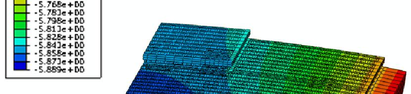
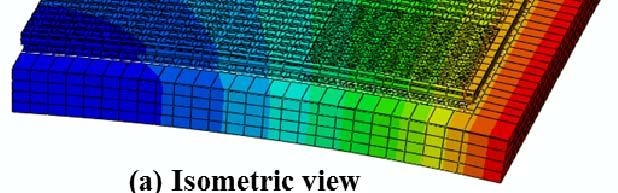
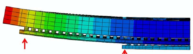
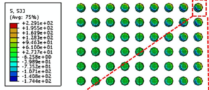
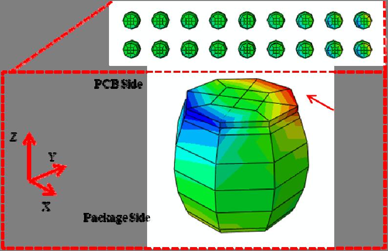
4 Figure 4. Deformation of at RDL-first-FOWLP PoP at the center of PCB due to bending effects. Figure 5. Peeling stress σ 33 of 9 9 solder joints array at the corner of bottom RDL-first-FOWLP. 1199


5 Figure 6. Peeling stress σ 33 on the dielectrics at the corner of bottom RDL-first-FOWLP. Figure 6 shows peeling stress σ 33 contour on the dielectrics at the corner of bottom RDL-first-FOWLP. The maximum peeling stress σ 33 induced to the dielectrics is about 104 MPa. The critical location is under the Cu pad at package corner. Delamination may be induced to the interface due to highly peeling stress. Figure 7 shows the peeling stress σ 33 contour of 3 3 solder joints array at the corner of top WLCSP. Due to the bending effects of PCB and bottom package, as illustrated in Figure 4, the solder joints at package edge of WLCSP suffered high peeling stress. Maximum peeling stress σ 33 induced to solder joints at the package edge WLCSP is about 253 MPa. The critical location for the solder joint is on the RDL side. Figure 7. Peeling stress σ 33 of 3 3 solder joints array at the corner of top WLCSP. IV. DROP TESTING AND FAILURE MECHANISM ANALYSIS RDL-first-FOWLP PoP test vehicle was mounted on the PCB for drop impact test as shown in Figure 8. Locations of the packages mounted on the PCB were defined as U1 to U5 with U3 at package center. No underfill was adopted for the RDL-first-FOWLP PoP test vehicle. During the drop impact testing, the PCB with five packages was installed on the drop tester table with supporting bolts at four corners. A half sine shock pulse loading was applied with the condition of 1500 g/0.5 ms. Resistance of the designed daisy chains was monitored during the drop testing. 1200


6 Figure 8. RDL-first-FOWLP PoP test vehicles mounted on the PCB. Table III shows test results of RDL-first-FOWLP PoP test vehicle on three PCB for 200 drops test. The testing results shows that all the samples can 30 times of drop test as required for mobile applications. Some packages can 200 times of drop test. By these drop impact tests, the reliability of RDL-first-FOWLP PoP test vehicle was validated. adhesion of the interface. From the picture, it can be seen that no failure happened to vertical Cu wire interconnection under drop impact loading. Cross section along the edge of bottom RDL-first- FOWLP was also conducted. Figure 10 shows the cross section SEM picture. It is can be observed that Cu pad was peeled off from the dielectrics layer. Crack was induced to dielectrics layer at the Cu pad edge. Large deformation also happened to the Cu pad due to peeling effects. Delamination induced to the interface of Cu pad/dielectrics was also caused by highly peeling stress and poor adhesion of the interface. Delamination happened to the interface of Cu pad /dielectrics and the interface of dielectrics/ EMC causing the critical issues to the drop impact reliability of FOWLP. The adhesion of the interfaces needs to be enhanced to withstand the peeling stress causing by bending effects of drop impact. TABLE III. VEHICEL. DROP TEST RESULTS OF RDL-FIRST-FOWLP POP TEST Location Sample 1 Sample 2 Sample drops 170 drops U1 U2 200 drops 200 drops U3 50 drops 50 drops U4 110 drops 50 drops U5 170 drops Some early failures were found for RDL-first-FOWLP PoP under drop impact loading. Cross section was conducted by the method of mechanical grinding followed by fine polishing. The mechanisms of the early failed daisy chains are shown in Figures 9, 10 and 11. Cross section along the corner of bottom RDL-first- FOWLP was conducted. SEM picture of cross section along the failed solder joint at the corner of bottom RDL-first- FOWLP is illustrated in Figure 9. Delamination induced to the interface of Cu pad/dielectrics layer can be seen from the picture. The Cu pad and trace was peeled off. Crack happened to Cu trace. Delamination induced to the interface of Cu pad/dielectrics is due to highly peeling stress and poor Figure 9. Failure mechanisms of critical solder joint at the corner of bottom RDL-first-FOWLP with details of Cu pad peeling and Cu trace cracking. 1201


7 Figure 11. Failure mechanisms of the package edge solder joints of top WLCSP with details of cracking on RDL side. Figure 11 shows failure mechanisms of the failed solder joints at the package edge of top WLCSP. It can be found that cracks happened to solder joints on back RDL side under 1500 G drop test loading. It can also be found that insufficient wetting happened between the solder joints and the UBM on back RDL side. The cracks can happpen to the solder joints more easily with the insufficient wetting under the highly peeling stress as shown in Figure 7. Figure 10. Failure mechanisms of critical solder joint at the edge of bottom RDL-first-FOWLP with details of Cu pad peeling and dielectrics cracking. V. CONCLUSIONS In this paper, reliability of 20 mm 20 mm RDL-first- FOWLP on bottom and 8 mm 8 mm WLCSP on top for PoP test vehicle under drop impact loading was validated by the experimental testing. The failure mechanisms were identified by cross section observation. Some important conclusions are summarized as following: (1) Drop impact reliability of 20 mm 20 mm RDL-first- FOWLP PoP test vehicle was validated by 1500 G/0.5 ms drop impact tests. The samples can 30 times of drop test and some packages can 200 times of drop test. (2) Failure mechanisms of the early failed samples were identified to be Cu pad peeling off, cracking of dielectrics and Cu trace of the bottom RDL-first- FOWLP and cracks on the edge solder joint of top WLCSP. (3) Delamination was induced on the interface of Cu pad/dielectrics by highly peeling stress due to bending effects. The adhesion of Cu pad to dielectrics layer need to be enhanced to avoid happening of delamination. 1202
8 (4) Highly peeling stress was induced to the package edge/corner solder joints of top WLCSP due to the bending effects of PCB and bottom package. ACKNOWLEDGMENT The supports from the project High Density Fan-Out Wafer Level Packaging (HD-FOWLP) Consortium are greatly appreciated in terms of participation in discussions and encouragement from members. REFERENCES [1] M. Brunnbauer. T. Meyer. G. Ofner. K. Mueller. R. Hagen, Embedded Wafer Level Ball Grid Array (ewlb), 33rd International Electronics Manufacturing Teclmology Conference, 2008, pp [2] B. Keser, C. Amrine, T. Duong, O. Fay, S. Hayes, G. Leal, W.Lytle, D. Mitchell, R.Wenzel, The Redistributed Chip Package: A Breakthrough for Advanced Packaging, Electronic Components and Technology Conference, 2007, pp [3] K. Liu, B.Adams, and S.W. Yoon, Integration Through Wafer-Level Packaging Approach, 2015 International Wafer Level Packaging Conference (IWLPC) Proceedings, [4] J. H. Lau, Patent Issues Of Embedded Fan-Out Wafer/Panel Level Packaging, Semiconductor Technology International Conference (CSTIC) China, [5] J.E. Luan and T. Y. Tee, Novel Board Level Drop Test Simulation using Implicit Transient Analysis with Input-G Method, Electronics Packaging Technology Conference, 2004, pp [6] E.H. Wong, C.S. Selvanayagam, S.K.W. Seah, W.D. van Driel, J.F.J.M. Caers, X.J. Zhao, N. Owens, L.C. Tan, D.R. Frear, M. Leoni, Y.S. Lai, and C.L. Yeh, Stress strain characteristics of Tin based solder alloys for drop impact modeling, J. of Electron. Mater., vol. 37, no. 6, pp ,
ADVANCED BOARD LEVEL MODELING FOR WAFER LEVEL PACKAGES
 As originally published in the SMTA Proceedings ADVANCED BOARD LEVEL MODELING FOR WAFER LEVEL PACKAGES Tiao Zhou, Ph.D. Southern Methodist University Dallas, TX, USA tiaoz@smu.edu Zhenxue Han, Ph.D. University
1 INTRODUCTION 2 SAMPLE PREPARATIONS
 Chikage NORITAKE This study seeks to analyze the reliability of three-dimensional (3D) chip stacked packages under cyclic thermal loading. The critical areas of 3D chip stacked packages are defined using
Reliability analysis of different structure parameters of PCBA under drop impact
 Journal of Physics: Conference Series PAPER OPEN ACCESS Reliability analysis of different structure parameters of PCBA under drop impact To cite this article: P S Liu et al 2018 J. Phys.: Conf. Ser. 986
Reliability assessment for Cu/Low-k structure based on bump shear modeling and simulation method
 Reliability assessment for Cu/Low-k structure based on bump shear modeling and simulation method Abstract Bump shear is widely used to characterize interface strength of Cu/low-k structure. In this work,
FEM Analysis on Mechanical Stress of 2.5D Package Interposers
 Hisada et al.: FEM Analysis on Mechanical Stress of 2.5D Package Interposers (1/8) [Technical Paper] FEM Analysis on Mechanical Stress of 2.5D Package Interposers Takashi Hisada, Toyohiro Aoki, Junko Asai,
Prediction of Encapsulant Performance Toward Fatigue Properties of Flip Chip Ball Grid Array (FC-BGA) using Accelerated Thermal Cycling (ATC)
 using Accelerated Thermal Cycling (ATC)") Prediction of Encapsulant Performance Toward Fatigue Properties of Flip Chip Ball Grid Array (FC-BGA) using Accelerated Thermal Cycling (ATC) ZAINUDIN KORNAIN 1, AZMAN JALAR 2,3, SHAHRUM ABDULLAH 3, NOWSHAD
Prediction of Encapsulant Performance Toward Fatigue Properties of Flip Chip Ball Grid Array (FC-BGA) using Accelerated Thermal Cycling (ATC) ZAINUDIN KORNAIN 1, AZMAN JALAR 2,3, SHAHRUM ABDULLAH 3, NOWSHAD
Cyclic Bend Fatigue Reliability Investigation for Sn-Ag-Cu Solder Joints
 Cyclic Bend Fatigue Reliability Investigation for Sn-Ag-Cu Solder Joints F.X. Che* 1, H.L.J. Pang 2, W.H. Zhu 1 and Anthony Y. S. Sun 1 1 United Test & Assembly Center Ltd. (UTAC) Packaging Analysis &
Modal and Harmonic Response Analysis of PBGA and S-N Curve Creation of Solder Joints
 Sensors & Transducers 2013 by IFSA http://www.sensorsportal.com Modal and Harmonic Response Analysis of PBGA and S-N Curve Creation of Solder Joints 1 Yu Guo, 1 Kailin Pan, 1, 2 Xin Wang, 1, 2 Tao Lu and
Assessment of Current Density Singularity in Electromigration of Solder Bumps
 Assessment of Current Density Singularity in Electromigration of Solder Bumps Pridhvi Dandu and Xuejun Fan Department of Mechanical Engineering Lamar University PO Box 10028, Beaumont, TX 77710, USA Tel:
Ultrasonic Anisotropic Conductive Films (ACFs) Bonding of Flexible Substrates on Organic Rigid Boards at Room Temperature
 Bonding of Flexible Substrates on Organic Rigid Boards at Room Temperature") Ultrasonic Anisotropic Conductive Films (ACFs) Bonding of Flexible Substrates on Organic Rigid Boards at Room Temperature Kiwon Lee, Hyoung Joon Kim, Il Kim, and Kyung Wook Paik Nano Packaging and Interconnect
Ultrasonic Anisotropic Conductive Films (ACFs) Bonding of Flexible Substrates on Organic Rigid Boards at Room Temperature Kiwon Lee, Hyoung Joon Kim, Il Kim, and Kyung Wook Paik Nano Packaging and Interconnect
314 IEEE TRANSACTIONS ON ADVANCED PACKAGING, VOL. 33, NO. 2, MAY Wei Tan, I. Charles Ume, Ying Hung, and C. F. Jeff Wu
 314 IEEE TRANSACTIONS ON ADVANCED PACKAGING, VOL. 33, NO. 2, MAY 2010 Effects of Warpage on Fatigue Reliability of Solder Bumps: Experimental and Analytical Studies Wei Tan, I. Charles Ume, Ying Hung,
Failure Mechanism for fine pitch micro bump in Cu/Sn/Cu system during Current Stressing
 Failure Mechanism for fine pitch micro bump in Cu/Sn/Cu system during Current Stressing Hsiao Hsiang Yao, Alastair David Trigg, and Chai Tai Chong Institute of Microelectronics, A*STAR (Agency for Science,
TRENDS IN LEVENSDUURTESTEN VOOR MICRO-ELEKTRONICA PLOT CONFERENTIE
 TRENDS IN LEVENSDUURTESTEN VOOR MICRO-ELEKTRONICA PLOT CONFERENTIE JEROEN JALINK 8 JUNI 2016 MICROELECTRONICS RELIABILITY 54 (2014) 1988 1994 Contents Introduction NXP Package form factor Failure mechanism
Process Modeling and Thermal/Mechanical Behavior of ACA/ACF Type Flip-Chip Packages
 Process Modeling and Thermal/Mechanical Behavior of ACA/ACF Type Flip-Chip Packages K. N. Chiang Associate Professor e-mail: knchiang@pme.nthu.edu.tw C. W. Chang Graduate Student C. T. Lin Graduate Student
Woon-Seong Kwon Myung-Jin Yim Kyung-Wook Paik
 Woon-Seong Kwon e-mail: wskwon@kaist.ac.kr Myung-Jin Yim Kyung-Wook Paik Department of Materials Science and Engineering Korea Advanced Institute of Science and Technology Daejon 305-701, Korea Suk-Jin
Mechanical Simulations for Chip Package Interaction: Failure Mechanisms, Material Characterization, and Failure Data
 Mechanical Simulations for Chip Package Interaction: Failure Mechanisms, Material Characterization, and Failure Data Ahmer Syed Amkor Technology Enabling a Microelectronic World Outline Effect of Chip
DROP TEST performance has been one of the key package
 1802 IEEE TRANSACTIONS ON COMPONENTS, PACKAGING AND MANUFACTURING TECHNOLOGY, VOL. 2, NO. 11, NOVEMBER 2012 Finite Element Modeling of System Design and Testing Conditions for Component Solder Ball Reliability
Stress in Flip-Chip Solder Bumps due to Package Warpage -- Matt Pharr
 Stress in Flip-Chip Bumps due to Package Warpage -- Matt Pharr Introduction As the size of microelectronic devices continues to decrease, interconnects in the devices are scaling down correspondingly.
The Reliability Analysis and Structure Design for the Fine Pitch Flip Chip BGA Packaging
 The Reliability Analysis and Structure Design for the Fine Pitch Flip Chip BGA Packaging Chih-Tang Peng 1, Chang-Ming Liu 1, Ji-Cheng Lin 1, Kuo-Ning Chiang E-Mail: Knchiang@pme.nthu.edu.tw Department
Impact of Uneven Solder Thickness on IGBT Substrate Reliability
 Impact of Uneven Solder Thickness on IGBT Substrate Reliability Hua Lu a, Chris Bailey a, Liam Mills b a Department of Mathematical Sciences, University of Greenwich 30 Park Row, London, SE10 9LS, UK b
Temperature Cycling Analysis of Lead-Free Solder Joints in Electronic Packaging
 Temperature Cycling Analysis of Lead-Free Solder Joints in Electronic Packaging Shan Li a,*, Zhenyu Huang a and Jianfeng Wang a,shaowu Gao b a Intel (Shanghai) Technology Development Ltd., Shanghai, China
Microelectronics Reliability
 Microelectronics Reliability 51 (211) 1385 1392 Contents lists available at ScienceDirect Microelectronics Reliability journal homepage: www.elsevier.com/locate/microrel Characterization of elasto-plastic
TABLE OF CONTENTS CHAPTER TITLE PAGE DECLARATION DEDICATION ACKNOWLEDGEMENT ABSTRACT ABSTRAK
 vii TABLE OF CONTENTS CHAPTER TITLE PAGE DECLARATION DEDICATION ACKNOWLEDGEMENT ABSTRACT ABSTRAK TABLE OF CONTENTS LIST OF TABLES LIST OF FIGURES LIST OF ABBREVIATIONS LIST OF SYMBOLS ii iii iv v vi vii
CLCC Solder Joint Life Prediction under Complex Temperature Cycling Loading
 CLCC Solder Joint Life Prediction under Complex Temperature Cycling Loading, Michael Osterman, and Michael Pecht Center for Advanced Life Cycle Engineering (CALCE) University of Maryland College Park,
SOLDER JOINT RELIABILITY IN ELECTRONICS UNDER SHOCK AND VIBRATION USING EXPLICIT FINITE-ELEMENT SUB-MODELING. Sameep Gupte
 SOLDER JOINT RELIABILITY IN ELECTRONICS UNDER SHOCK AND VIBRATION USING EXPLICIT FINITE-ELEMENT SUB-MODELING Except where reference is made to the work of others, the work described in this thesis is my
Thermal aspects of 3D and 2.5D integration
 Thermal aspects of 3D and 2.5D integration Herman Oprins Sr. Researcher Thermal Management - imec Co-authors: Vladimir Cherman, Geert Van der Plas, Eric Beyne European 3D Summit 23-25 January 2017 Grenoble,
Simulation of the Influence of Manufacturing Quality on Thermomechanical Stress of Microvias
 As originally published in the IPC APEX EXPO Conference Proceedings. Simulation of the Influence of Manufacturing Quality on Thermomechanical Stress of Microvias Yan Ning, Michael H. Azarian, and Michael
Next-Generation Packaging Technology for Space FPGAs
 Power Matters. Next-Generation Packaging Technology for Space FPGAs Microsemi Space Forum Russia November 2013 Raymond Kuang Director of Packaging Engineering, SoC Products Group Agenda CCGA (ceramic column
On the difference between thermal cycling and thermal shock testing for board level reliability of soldered interconnections
 Microelectronics Reliability 47 (27) 444 449 www.elsevier.com/locate/microrel On the difference between thermal cycling and thermal shock testing for board level reliability of soldered interconnections
Dynamic Strain of Ultrasonic Cu and Au Ball Bonding Measured In-Situ by Using Silicon Piezoresistive Sensor
 2017 IEEE 67th Electronic Components and Technology Conference Dynamic Strain of Ultrasonic Cu and Au Ball Bonding Measured In-Situ by Using Silicon Piezoresistive Sensor Keiichiro Iwanabe, Kenichi Nakadozono,
Delamination Modeling for Power Packages and Modules. Rainer Dudek, R. Döring, S. Rzepka Fraunhofer ENAS, Micro Materials Center Chemnitz
 Delamination Modeling for Power Packages and Modules Rainer Dudek, R. Döring, S. Rzepka Fraunhofer ENAS, Micro Materials Center Chemnitz The Micro Materials Center @ Virtual Prototyping Finite Element
Characteristics of Thermosonic Anisotropic Conductive Adhesives (ACFs) Flip-Chip Bonding
 Flip-Chip Bonding") Materials Transactions, Vol. 51, No. 10 (2010) pp. 1790 to 1795 Special Issue on Lead-Free and Advanced Interconnection Materials for Electronics #2010 The Japan Institute of Metals Characteristics of
Materials Transactions, Vol. 51, No. 10 (2010) pp. 1790 to 1795 Special Issue on Lead-Free and Advanced Interconnection Materials for Electronics #2010 The Japan Institute of Metals Characteristics of
MICROCSP is an ADI wafer level chip scale package, the
 IEEE TRANSACTIONS ON COMPONENTS AND PACKAGING TECHNOLOGIES, VOL. 28, NO. 3, SEPTEMBER 2005 441 Effect of Geometry and Temperature Cycle on the Reliability of WLCSP Solder Joints Satish C. Chaparala, Brian
F. G. Marín, D Whalley, H Kristiansen and Z. L. Zhang, Mechanical Performance of Polymer Cored BGA Interconnects, Proceedings of the 10th Electronics
 F. G. Marín, D Whalley, H Kristiansen and Z. L. Zhang, Mechanical Performance of Polymer Cored BGA Interconnects, Proceedings of the 1th Electronics Packaging Technology Conference, 28. Mechanical Performance
Chapter 5: Ball Grid Array (BGA)
") Chapter 5: Ball Grid Array (BGA) 5.1 Development of the Models The following sequence of pictures explains schematically how the FE-model of the Ball Grid Array (BGA) was developed. Initially a single
Chapter 5: Ball Grid Array (BGA) 5.1 Development of the Models The following sequence of pictures explains schematically how the FE-model of the Ball Grid Array (BGA) was developed. Initially a single
Sensitivity analysis on the fatigue life of solid state drive solder joints by the finite element method and Monte Carlo simulation
 https://doi.org/10.1007/s00542-018-3819-0 (0456789().,-volV)(0456789().,-volV) TECHNICAL PAPER Sensitivity analysis on the fatigue life of solid state drive solder joints by the finite element method and
CHIP/PACKAGE CO-ANALYSIS OF THERMAL-INDUCED STRESS FOR FAN-OUT WAFER LEVEL PACKAGING
 CHIP/PACKAGE CO-ANALYSIS OF THERMAL-INDUCED STRESS FOR FAN-OUT WAFER LEVEL PACKAGING Stephen Pan, Zhigang Feng, Norman Chang ANSYS, Inc. San Jose, CA, USA stephen.pan, zhigang.feng, nchang@ansys.com ABSTRACT
Effect of Direction of Ultrasonic Vibration on Flip-Chip Bonding
 Transactions of The Japan Institute of Electronics Packaging Vol. 6, No. 1, 13 [Technical Paper] Effect of Direction of Ultrasonic Vibration on Flip-Chip Bonding Mutsumi Masumoto*, Yoshiyuki Arai*, **,
THE demand for plastic packages has increased due to
 294 IEEE TRANSACTIONS ON COMPONENTS AND PACKAGING TECHNOLOGIES, VOL. 30, NO. 2, JUNE 2007 Predictive Model for Optimized Design Parameters in Flip-Chip Packages and Assemblies Seungbae Park, H. C. Lee,
Study of Electromigration of flip-chip solder joints using Kelvin probes
 Study of Electromigration of flip-chip solder joints using Kelvin probes Y. W. Chang and Chih Chen National Chiao Tung University, Department of Material Science & Engineering, Hsin-chu 30010, Taiwan,
A Numerical Approach Towards the Correlation Between Ball Impact Test and Drop Reliability
 A Numerical Approach Towards the Correlation Between Ball Impact Test and Drop Reliability Chang-Lin Yeh*, Yi-Shao Lai Stress-Reliability Lab, Advanced Semiconductor Engineering, Inc. 26 Chin 3 rd Rd.,
Temperature-dependent Thermal Stress Determination for Through-Silicon-Vias (TSVs) by Combining Bending Beam Technique with Finite Element Analysis
 by Combining Bending Beam Technique with Finite Element Analysis") Temperature-dependent Thermal Stress Determination for Through-Silicon-Vias (TSVs) by Combining Bending Beam Technique with Finite Element Analysis Kuan H. Lu, Suk-Kyu Ryu*, Qiu Zhao, Klaus Hummler**,
Temperature-dependent Thermal Stress Determination for Through-Silicon-Vias (TSVs) by Combining Bending Beam Technique with Finite Element Analysis Kuan H. Lu, Suk-Kyu Ryu*, Qiu Zhao, Klaus Hummler**,
Thermo-structural Model of Stacked Field-programmable Gate Arrays (FPGAs) with Through-silicon Vias (TSVs)
 with Through-silicon Vias (TSVs)") Manuscript for Review Thermo-structural Model of Stacked Field-programmable Gate Arrays (FPGAs) with Through-silicon Vias (TSVs) Journal: Electronics Letters Manuscript ID: draft Manuscript Type: Letter
Manuscript for Review Thermo-structural Model of Stacked Field-programmable Gate Arrays (FPGAs) with Through-silicon Vias (TSVs) Journal: Electronics Letters Manuscript ID: draft Manuscript Type: Letter
TCAD Modeling of Stress Impact on Performance and Reliability
 TCAD Modeling of Stress Impact on Performance and Reliability Xiaopeng Xu TCAD R&D, Synopsys March 16, 2010 SEMATECH Workshop on Stress Management for 3D ICs using Through Silicon Vias 1 Outline Introduction
Multilayer Wiring Technology with Grinding Planarization of Dielectric Layer and Via Posts
 Tani et al.: Multilayer Wiring Technology with Grinding Planarization (1/6) [Technical Paper] Multilayer Wiring Technology with Grinding Planarization of Dielectric Layer and Via Posts Motoaki Tani, Kanae
Available online at ScienceDirect. XVII International Colloquium on Mechanical Fatigue of Metals (ICMFM17)
") Available online at www.sciencedirect.com ScienceDirect Procedia Engineering 74 ( 2014 ) 165 169 XVII International Colloquium on Mechanical Fatigue of Metals (ICMFM17) Fatigue of Solder Interconnects
Available online at www.sciencedirect.com ScienceDirect Procedia Engineering 74 ( 2014 ) 165 169 XVII International Colloquium on Mechanical Fatigue of Metals (ICMFM17) Fatigue of Solder Interconnects
Simulation Analysis of Microchannel Deformation during LTCC Warm Water Isostatic Pressing Process Lang Ping, Zhaohua Wu*
 International Conference on Information Sciences, Machinery, Materials and Energy (ICISMME 2015) Simulation Analysis of Microchannel Deformation during LTCC Warm Water Isostatic Pressing Process Lang Ping,
Key words Lead-free solder, Microelectronic packaging, RF packaging, RoHS compliant, Solder joint reliability, Weibull failure distribution
 Solder Joint Reliability Assessment for a High Performance RF Ceramic Package Paul Charbonneau, Hans Ohman, Marc Fortin Sanmina Corporation 500 Palladium Dr. Ottawa, Ontario K2V 1C2 Canada Ph: 613-886-6000;
Impact of BGA Warpage on Quality. Mike Varnau
 Impact of BGA Warpage on Quality Mike Varnau 5-11-06 Contents What is a Ball in Cup Failure Case Study Background Problem Identification Solution Results Assembly Related Factors Causing Ball in Cup Component
Copyright 2008 Year IEEE. Reprinted from IEEE TRANSACTIONS ON COMPONENTS AND PACKAGING TECHNOLOGIES, VOL. 31, NO. 1, MARCH Such permission of
 Copyright 2008 Year IEEE. Reprinted from IEEE TRANSACTIONS ON COMPONENTS AND PACKAGING TECHNOLOGIES, VOL. 31, NO. 1, MARCH 2008. Such permission of the IEEE does not in any way imply IEEE endorsement of
Deformation of solder joint under current stressing and numerical simulation II
 International Journal of Solids and Structures 41 (2004) 4959 4973 www.elsevier.com/locate/ijsolstr Deformation of solder joint under current stressing and numerical simulation II Hua Ye *, Cemal Basaran,
Four-point bending cycling as alternative for Thermal cycling solder fatigue testing
 Four-point bending as alternative for Thermal solder fatigue testing Bart Vandevelde a, Filip Vanhee b, Davy Pissoort b, Lieven Degrendele c, Johan De Baets c, Bart Allaert d, Ralph Lauwaert e, Riet Labie
Passionately Innovating With Customers To Create A Connected World
 Passionately Innovating With Customers To Create A Connected World Multi Die Integration Can Material Suppliers Meet the Challenge? Nov 14, 2012 Jeff Calvert - R&D Director, Advanced Packaging Technologies
Especial Bump Bonding Technique for Silicon Pixel Detectors
 Especial Bump Bonding Technique for Silicon Pixel Detectors E. Cabruja, M. Bigas, M. Ullán, G. Pellegrini, M. Lozano Centre Nacional de Microelectrònica Spain Outline Motivation Summary of bump bonding
884 IEEE TRANSACTIONS ON COMPONENTS, PACKAGING AND MANUFACTURING TECHNOLOGY, VOL. 2, NO. 5, MAY 2012
 884 IEEE TRANSACTIONS ON COMPONENTS, PACKAGING AND MANUFACTURING TECHNOLOGY, VOL. 2, NO., MAY 212 Ultrasonic Bonding of Anisotropic Conductive Films Containing Ultrafine Solder Balls for High-Power and
Tools for Thermal Analysis: Thermal Test Chips Thomas Tarter Package Science Services LLC
 Tools for Thermal Analysis: Thermal Test Chips Thomas Tarter Package Science Services LLC ttarter@pkgscience.com INTRODUCTION Irrespective of if a device gets smaller, larger, hotter or cooler, some method
Assessment of Soft Errors due to Alpha Emissions from Presolder on Flip Chip Devices Rick Wong, Shi-Jie Wen, Peng Su, Li Li 10/30/09
 Assessment of Soft Errors due to Alpha Emissions from Presolder on Flip Chip Devices Rick Wong, Shi-Jie Wen, Peng Su, Li Li 10/30/09 1 Introduction Cause of Soft errors a. Ion creates electron hole pairs
Interfacial delamination and fatigue life estimation of 3D solder bumps in flip-chip packages
 Microelectronics Reliability 44 (004) 471 483 www.elsevier.com/locate/microrel Interfacial delamination and fatigue life estimation of 3D solder bumps in flip-chip packages Yu Gu, Toshio Nakamura * Department
Fatigue Life Evaluation of Lead-free Solder under Thermal and Mechanical Loads
 Fatigue Life Evaluation of Lead-free Solder under Thermal and Mechanical Loads Ilho Kim and Soon-Bok Lee* Department of Mechanical Engineering, Korea Advanced Institute of Science and Technology 373-,
THERMOMECHANICAL ANALYSIS OF ELECTRONIC PACKAGE USING FINITE ELEMENT METHOD
 THERMOMECHANICAL ANALYSIS OF ELECTRONIC PACKAGE USING FINITE ELEMENT METHOD N.BhargavaRamudu 1, V. Nithin Kumar Varma 2, P.Ravi kiran 3, T.Venkata Avinash 4, Ch. Mohan Sumanth 5, P.Prasanthi 6 1,2,3,4,5,6
Fluxless Soldering in Activated Hydrogen Atmosphere
 Fluxless Soldering in Activated Hydrogen Atmosphere C. Christine Dong1*, Richard E. Patrick1, Russell A. Siminski 1, and Tim Bao 2 1 Air Products and Chemicals, Allentown, PA 18195-1501, USA 2 Air Products
Drop Test Simulation of a BGA Package: Methods & Experimental Comparison
 Drop Test Simulation of a BGA Package: Methods & Experimental Comparison Chris Cowan, Ozen Engineering, Inc. Harvey Tran, Intel Corporation Nghia Le, Intel Corporation Metin Ozen, Ozen Engineering, Inc.
SCB10H Series Pressure Elements PRODUCT FAMILY SPEFICIFATION. Doc. No B
 PRODUCT FAMILY SPEFICIFATION SCB10H Series Pressure Elements SCB10H Series Pressure Elements Doc. No. 82 1250 00 B Table of Contents 1 General Description... 3 1.1 Introduction... 3 1.2 General Description...
Effects of underfill material on solder deformation and damage in 3D packages
 University of New Mexico UNM Digital Repository Mechanical Engineering ETDs Engineering ETDs 9-3-2013 Effects of underfill material on solder deformation and damage in 3D packages Geno Flores Follow this
The Increasing Importance of the Thermal Management for Modern Electronic Packages B. Psota 1, I. Szendiuch 1
 Ročník 2012 Číslo VI The Increasing Importance of the Thermal Management for Modern Electronic Packages B. Psota 1, I. Szendiuch 1 1 Department of Microelectronics, Faculty of Electrical Engineering and
The Use of COMSOL Multiphysics for Studying the Fracture Pressure of Rectangular Micro-Channels Embedded in Thin Silicon Substrates
 The Use of COMSOL Multiphysics for Studying the Fracture Pressure of Rectangular Micro-Channels Embedded in Thin Silicon Substrates Kaitlin Howell 1, H. Georgiou 2, A. Mapelli 3, P. Petagna 3, G. Romagnoli
Electrical Conductive Adhesives with Nanotechnologies
 Yi Li Daniel Lu C.P. Wong Electrical Conductive Adhesives with Nanotechnologies Springer 1 Introduction 1 1.1 Electronics Packaging and Interconnect 1 1.2 Interconnection Materials 11 1.2.1 Lead-Free Interconnect
Dynamic behaviour of electronics package and impact reliability of BGA solder joints
 Dynamic behaviour of electronics package and impact reliability of BGA solder joints Q YU1, H Kikuchil, S Ikedal, M Shiratoril, M Kakino2, N Fujiwara2 Department of Mechanical Engineering and Material
A Note on Suhir s Solution of Thermal Stresses for a Die-Substrate Assembly
 M. Y. Tsai e-mail: mytsai@mail.cgu.edu.tw C. H. Hsu C. N. Han Department of Mechanical Engineering, Chang Gung University, Kwei-Shan, Tao-Yuan, Taiwan 333, ROC A Note on Suhir s Solution of Thermal Stresses
Influence of Plating Quality on Reliability of Microvias
 As originally published in the IPC APEX EXPO Conference Proceedings. Influence of Plating Quality on Reliability of Microvias Yan Ning, Michael H. Azarian, and Michael Pecht Center for Advanced Life Cycle
Critical Issues in Computational Modeling and Fatigue Life Analysisfor PBGA Solder Joints
 Critical Issues in Computational Modeling and Fatigue Life Analysis for PBGA Solder Joints Critical Issues in Computational Modeling and Fatigue Life Analysisfor PBGA Solder Joints Xiaowu Zhang and S-W.
Budapest, Hungary, September 2007 The Characteristics of Electromigration And Thermomigration in Flip Chip Solder Joints
 The Characteristics of Electromigration And Thermomigration in Flip Chip Solder Joints Dan Yang and Y. C. Chan* Department of Electronic Engineering, City University of Hong Kong, 83 Tat Chee Avenue, Kowloon,
LPSC424.xxx Low Profile Silicon Capacitor
 LPSC424.xxx - 42 Low Profile Silicon Capacitor Rev 3. Key features Ultra low profile (1µm) High stability of capacitance value: Temperature
Prognostics implementation of electronics under vibration loading
 Available online at www.sciencedirect.com Microelectronics Reliability 7 (7) 89 856 www.elsevier.com/locate/microrel Prognostics implementation of electronics under vibration loading Jie Gu *, Donald Barker,
WTSC144.xxx Wire Bonding Temperature Silicon Vertical Capacitor
 WTSC144.xxx Wire Bonding Temperature Silicon Vertical Capacitor Rev 3.1 Key features Full compatible to monolithic ceramic capacitors Ultra high stability of capacitance value: Temperature ±1.5% (-55 C
Thermal-Mechanical Analysis of a Different Leadframe Thickness of Semiconductor Package under the Reflow Process
 American Journal of Applied Sciences 6 (4): 616-625, 2009 ISSN 1546-9239 2009 Science Publications Thermal-Mechanical Analysis of a Different Leadframe Thickness of Semiconductor Package under the Reflow
Chapter 7 Mechanical Characterization of the Electronic Packages
 Chapter 7 Mechanical Characterization of the Electronic Packages 1 3 Thermal Mismatch Si (CTE=~3 ppm/c) Underfill (CTE=7 ppm/c) EU solder (CTE=5 ppm/c) Substrate (CTE=15~0 ppm/c) Thermal mismatch in electronic
Nonlinear Time and Temperature Dependent Analysis of the Lead-Free Solder Sealing Ring of a Photonic Switch
 Nonlinear Time and Temperature Dependent Analysis of the Lead-Free Solder Sealing Ring of a Photonic Switch J. Lau, Z. Mei, S. Pang, C. Amsden, J. Rayner and S. Pan Agilent Technologies, Inc. 5301 Stevens
Shorter Field Life in Power Cycling for Organic Packages
 Shorter Field Life in Power Cycling for Organic Packages S. B. Park e-mail: sbpark@binghamton.edu Izhar Z. Ahmed Department of Mechanical Engineering, State University of New York at Binghamton, Binghamton,
New Die Attach Adhesives Enable Low-Stress MEMS Packaging
 New Die Attach Adhesives Enable Low-Stress MEMS Packaging Dr. Tobias Königer DELO Industrial Adhesives DELO-Allee 1; 86949 Windach; Germany Tobias.Koeniger@DELO.de Phone +49 8193 9900 365 Abstract High
2017 IEEE 67th Electronic Components and Technology Conference
 2017 IEEE 67th Electronic Components and Technology Conference A Unique Temporary Bond Solution Based on a Polymeric Material Tacky at Room Temperature and Highly Thermally Resistant Application Extension
An Experimental Validation of Modelling for Pb-free Solder Joint Reliability
 NPL Report MATC (A) 11 An Experimental Validation of Modelling for Pb-free Solder Joint Reliability Miloš Dušek, Jaspal Nottay and Christopher Hunt Hua Lu, Christopher Bailey, University of Greenwich October
The Stress Field Characteristics in the Surface Mount Solder Joints under Temperature Cycling: Temperature Effect and Its Evaluation
 SUPPLEMENT TO THE WELDING JOURNL, JUNE 2002 Sponsored by the merican Welding Society and the Welding Research Council The Stress Field Characteristics in the Surface Mount Solder Joints under Temperature
Understanding Integrated Circuit Package Power Capabilities
 Understanding Integrated Circuit Package Power Capabilities INTRODUCTION The short and long term reliability of s interface circuits, like any integrated circuit, is very dependent on its environmental
Effect of under-bump-metallization structure on electromigration of Sn-Ag solder joints
 Advances in Materials Research, Vol. 1, No. 1 (2012) 83-92 83 Effect of under-bump-metallization structure on electromigration of Sn-Ag solder joints Hsiao-Yun Chen, Min-Feng Ku and Chih Chen* Department
Reliability Evaluation Method for Electronic Device BGA Package Considering the Interaction Between Design Factors
 Reliability Evaluation Method for Electronic Device BGA Package Considering the Interaction Between Design Factors Satoshi KONDO *, Qiang YU *, Tadahiro SHIBUTANI *, Masaki SHIRATORI * *Department of Mechanical
THERMAL PERFORMANCE EVALUATION AND METHODOLOGY FOR PYRAMID STACK DIE PACKAGES
 THERMAL PERFORMANCE EVALUATION AND METHODOLOGY FOR PYRAMID STACK DIE PACKAGES Krishnamoorthi.S, *W.H. Zhu, C.K.Wang, Siew Hoon Ore, H.B. Tan and Anthony Y.S. Sun. Package Analysis and Design Center United
Mechanical Analysis Challenges in Micro-Electronic Packaging
 Mechanical Analysis Challenges in Micro-Electronic Packaging Luke J. Garner, and Frank Z. Liang Intel Corporation Electrical and thermal performance enhancing features in modern integrated circuits have
Effects of hygrothermal aging on anisotropic conductive adhesive joints: experiments and theoretical analysis
 J. Adhesion Sci. Technol., Vol. 20, No. 12, pp. 1383 1399 (2006) VSP 2006. Also available online - www.brill.nl/jast Effects of hygrothermal aging on anisotropic conductive adhesive joints: experiments
Research Challenges and Opportunities. in 3D Integrated Circuits. Jan 30, 2009
 Jan 3, 29 Research Challenges and Opportunities in 3D Integrated Circuits Ankur Jain ankur.jain@freescale.com, ankurjain@stanfordalumni.org Freescale Semiconductor, Inc. 28. 1 What is Three-dimensional
Understanding Integrated Circuit Package Power Capabilities
 Understanding Integrated Circuit Package Power Capabilities INTRODUCTION The short and long term reliability of National Semiconductor s interface circuits like any integrated circuit is very dependent
Mechanical Implications of High Current Densities in Flip-chip Solder Joints
 Mechanical Implications of High Current Densities in Flip-chip Solder Joints HUA YE, CEMAL BASARAN AND DOUGLAS C. HOPKINS UB Electronic Packaging Laboratory University at Buffalo, SUNY Buffalo, NY 14260
Low-temperature Ultrasonic Bonding of Cu/Sn Microbumps with Au layer for High Density Interconnection Applications
 2017 IEEE 67th Electronic Components and Technology Conference Low-temperature Ultrasonic Bonding of Cu/Sn Microbumps with Au layer for High Density Interconnection Applications Qinghua Zeng, Yong Guan,
Flip Chip Reliability
 Flip Chip Reliability P e t e r B o r g e s e n, P h. D., S u r face Mount Laboratory, Corporation, Binghamton, New York 13902-0825 Daniel Blass, Sur f a c e M o u n t L a b o r a t o r y, U n i v e r
Effects of Chrome Pattern Characteristics on Image Placement due to the Thermomechanical Distortion of Optical Reticles During Exposure
 Effects of Chrome Pattern Characteristics on Image Placement due to the Thermomechanical Distortion of Optical Reticles During Exposure A. Abdo, ab L. Capodieci, a I. Lalovic, a and R. Engelstad b a Advanced
Modelling Methodology for Linear Elastic Compound Modelling Versus Visco-Elastic Compound Modelling
 Modelling Methodology for Linear Elastic Compound Modelling Versus Visco-Elastic Compound Modelling R.B.R van Silfhout 1), J.G.J Beijer 1), Kouchi Zhang 1), W.D. van Driel 2) 1) Philips Applied Technologies,
Mechanics of wafer bonding: Effect of clamping
 JOURNAL OF APPLIED PHYSICS VOLUME 95, NUMBER 1 1 JANUARY 2004 Mechanics of wafer bonding: Effect of clamping K. T. Turner a) Massachusetts Institute of Technology, Cambridge, Massachusetts 0219 M. D. Thouless
Supplementary Figure 1 shows overall fabrication process and detailed illustrations are given
 Supplementary Figure 1. Pressure sensor fabrication schematics. Supplementary Figure 1 shows overall fabrication process and detailed illustrations are given in Methods section. (a) Firstly, the sacrificial
A Micromechanics-Based Vapor Pressure Model in Electronic Packages
 X. J. Fan 1 Philips Research USA, 345 Scarborough Road, Briarcliff Manor, NY 10510 e-mail: xuejun.fan@ieee.org J. Zhou Department of Mechanical Engineering, Lamar University, Beaumont, TX 77710 e-mail:
Thermal Measurement and Simulation of the Component Rework Profile Temperature
 Thermal Measurement and Simulation of the Component Rework Profile Temperature J.T. Nurminen Oulu University of Applied Sciences, School of Engineering, Oulu, Finland janne.nurminen@osao.fi Abstract In