Nanotechnology. Nano From the Greek word for dwarf and means 10-9, or one-billionth. Here it refers to one-billionth of a meter, or 1 nanometer (nm).
|
|
|
- Tracey Johnston
- 6 years ago
- Views:
Transcription


 scale, making use of unique properties that occur for structures at those small")
1 Nanotechnology Nanotube transistor giga- billion mega- million kilo- thousand milli- one-thousandth micro- one-millionth nano- one-billionth Nano From the Greek word for dwarf and means 10-9, or one-billionth. Here it refers to one-billionth of a meter, or 1 nanometer (nm). 1 nanometer is about 3 atoms long. Nanotechnology Building and using materials, devices and machines at the nanometer (atomic/molecular) scale, making use of unique properties that occur for structures at those small dimensions. Most consider nanotechnology to be technology at the sub-micron scale: s of nanometers.


2 How small is a nanometer? (and other small sizes) Start with a centimeter. Now divide it into 10 equal parts. 1 cm 1 mm A centimeter is about the size of a bean. Each part is a millimeter long. About the size of a flea. Now divide that into 10 equal parts. 100 µm Each part is 100 micrometers long. About the size (width) of a human hair. Now divide that into 100 equal parts. Now divide that into 10 equal parts. 1 µm 100 nm Each part is a micrometer long. About the size of a bacterium. Each part is a 100 nanometers long. About the size of a virus. Finally divide that into 100 equal parts. 1 nm Each part is a nanometer. About the size of a few atoms or a small molecule.


 ~10 nm")


3 The Scale of Things Nanometers and More Things Natural 10-2 m 1 cm 10 mm Things Man-made Head of a pin 1-2 mm Dust mite 200 µm Human hair ~ µm wide Red blood cells (~7-8 µm) ~10 nm diameter Ant ~ 5 mm Fly ash ~ µm Nanoworld Microworld 10-3 m 10-4 m 10-5 m 10-6 m 10-7 m 10-8 m 1,000,000 nanometers = 1 millimeter (mm) Ultraviolet Visible Infrared Microwave 0.1 mm 100 µm 0.01 mm 10 µm 1,000 nanometers = 1 micrometer (µm) 0.1 µm 100 nm 0.01 µm 10 nm Pollen grain Red blood cells Zone plate x-ray lens Outer ring spacing ~35 nm MicroElectroMechanical (MEMS) devices µm wide Quantum corral of 48 iron atoms on copper surface positioned one at a time with an STM tip Corral diameter 14 nm Adopted from: Office of Basic Energy Sciences Office of Science, U.S. DOE Version , pmd Nanotube electrode ATP synthase 10-9 m 1 nanometer (nm) DNA ~2-1/2 nm diameter Atoms of silicon spacing nm m Soft x-ray 0.1 nm Intel computer chip and single transistor Smallest dimensions ~ 1nm Carbon nanotube ~1.3 nm diameter Carbon buckyball ~1 nm diameter Office of Basic Energy Sciences Office of Science, U.S. DOE Version , pmd


4 Why is Small Good? - Faster - Lighter - Can get into small spaces - Cheaper - More energy efficient - Less waste products, and uses less energy and materials to produce - Different properties at very small scale
5 - The melting point of gold decreases rapidly as the particle dimension reaches the nanometer scale. Melting point of gold as a function of gold particle diameter T melting ( o C) m.p. bulk Particle Diameter (nm) Reference: Buffat and Borel, Phys. Rev. A, vol. 13, p. 2287,1976.

6 The color of gold changes as the particle size changes at the nanometer scale. Chad Mirkin, Northwestern University, in NYTimes article by K. Chang
7 Why might properties of materials/structures be different at the nanoscale? Two of the reasons: 1. Ratio of surface area-to-volume of structure increases (most atoms are at or near the surface, which make them more weakly bonded and more reactive) 2. Quantum mechanical effects are important (size of structure is on same scale as the wavelengths of electrons, and quantum confinement occurs resulting in changes in electronic and optical properties)
 and as well as result in new properties and applications Can involve combinations of many types of")
8 Much of the motivating force and technology for nanotechnology came from the integrated circuit industry Intel s transistors As with the fabrication of integrated circuits (IC s), nanotechnology is based on building structures and systems at very small sizes Done to enhance performance (like IC s) and as well as result in new properties and applications Can involve combinations of many types of systems (mechanical, biological, chemical, optical, as well as electronic)

9 Examples of Nanotechnology Applications - Supercomputer in your palm, perhaps made from silicon nanowires, carbon nanotubes, or organic materials such as DNA - Very tiny motors, pumps, gyroscopes, and accelerometers; helicopters the size of flies or smaller - Tiny bio- and chemical-sensors; nanoparticles that track and destroy cancer cells; artificial body parts and implantable drug delivery systems - Energy storage (batteries) and conversion (solar cells) using nanowires and nanotubes - Enhanced consumer products using nano- whiskers, nanoparticles, and nanotubes for: stain and wrinkle resistant clothes, transparent zinc oxide sunscreen, fast-absorbing drugs and nutrients, extra-strong tennis racquets, and scratch-resistant paint
 MEMS and NEMS micro/nano")


10 Mite spinning on micromotor (Sandia National Labs) MEMS and NEMS micro/nano electromechanical systems Bugbot for traveling and taking photos in human digestive system (Carnegie Mellon University) World s smallest mobile robot, with no wheels, gears or hinged joints (Dartmouth College) Ant s leg strength and motion measured on microsensor, for robot development (Stanford)


 to coat medical tools, and")

11 Iron nanoparticles to clean poisons from water. Can also clean heavy metals from soil. (Lehigh University) Gold nanoparticles, coated with antibodies, and which fluoresce and heat up, can track and destroy cancer cells (University of Illinois, Georgia Tech, Rice, U. Texas, and UCSF) Using Nano-silver (solutions of silver nanoparticles) to coat medical tools, and in burn and surgical dressings, which protects against bacteria and fungus by inhibiting cellular metabolism and growth (Nanotech)


")


 Si or Ge")

12 Carbon nanotube (CNT) transistor for future computer chips (Stanford, UC Berkeley) First CNT computer built in SNF. Cover of prestigious Nature Magazine, 2013) Flat panel displays using carbon nanotubes as mini electron emitters instead of CRT s (Motorola, Samsung) Si or Ge nanowire batteries holding 10 times the charge of existing lithium-ion batteries (Stanford)

")

13 Carbon nanotube shag electrode in ultra-capacitors for energy storage (MIT) Silicon nanowires as solar cells, nanoelectronic power sources, and sensors (Stanford)


 Face Cream to attract")
14 Some Currently Available Nanotechnology Products Easton CNT (carbon nanotube) baseball bat ArcticShield stink-proof socks with silver nanoparticles Nano Wear sunblock with TiO 2 /ZnO 2 nanoparticles Nanopants that repel liquids by nanowhiskers attached to cloth fibers Zelens Fullerene C-60 (buckyball) Face Cream to attract and neutralise the damaging free radicals
15 How do you build something so small? Top-down building something by starting with a larger component and carving away material (like a sculpture). In nanotechnology: patterning (using photolithography) and etching away material, as in building integrated circuits Bottom-up building something by assembling smaller components (like building a car engine). In nanotechnology: self-assembly of atoms and molecules, as in chemical and biological systems

.")

16 How do you build something so small? Top-down building something by starting with a larger piece and carving away material (like a sculpture). Bottom-up building something by putting together smaller pieces (like building a car engine).


17 Top-down fabrication Method used by integrated circuit industry to fabricate computer chips down to ~ 15 nm size Makes use of depositing thin films, then photolithography and plasma etching to make films into desired patterns on a silicon wafer.


18 Top-down fabrication

19 Repeat process with different thin films and different patterns (each aligned to lower layer) to produce desired structure. Use scanning electron beam to produce masks with very small feature sizes.
.")
20 Limitations of top-down fabrication Due to diffraction effects, the practical limit for optical lithography is around 100 nm. Can use lithography and processing tricks to get feature sizes even smaller (as in Intel devices). To define much smaller features, electron beams, or ebeams, (which have smaller wavelengths) can be used. Feature sizes smaller than 15 nm can be patterned. But e-beam projection systems using masks have not been fully developed instead, direct-write e-beam lithography has been used. While optical lithography works in parallel over the wafer (with high throughput), direct-write e-beam lithography works as a series process (with very low throughput). An alternate method is bottom-up fabrication.


 Carbon nanotube growth")

 More extreme example:")
21 Bottom-up fabrication Adding atoms to atoms, molecules to molecules Self-assembly of atoms and molecules Use of chemical and biological processes Current day examples: Vertical growth of nanowires for electronic devices (Stanford) Carbon nanotube growth Self-assemble of organic monolayers for molecular transistors, etc. (Florida) Electric field aligning of nanowires (U. Mass) More extreme example: Self-replicating robots. Nanoparticles by flame pyrolysis (Princeton)

22 Bottom-up fabrication A way to make nanometer size features, and lots of them, letting nature work for you. But some challenges: Getting the structures to always grow exactly how and where you want them to Making complicated patterns Some common strategies: Ferromagnetic microparticles (Argonne Nat l. Lab) Use catalysts, stress fields, electric/magnetic fields, capillary forces, etc. to achieve selective growth or placement Use top-down processes in conjunction with bottom-up processes, and build on silicon substrates 22


23 How do you build something so small? Tools are needed to image, analyze, and manipulate very small features - Scanning Probe Microscopy, including the Atomic Force Microscope (AFM) laser photo detector cantilever probe AFM tip, used to manipulate, image and measure atomic scale features. probe tip sample surface piezoelectric stage


24 AFM image of mineral surface showing atomic structure. AFM image of carbon nanotube AFM image of human blood cells Other scanning probe microscopes measure other properties, such as electrical and magnetic. Positioning single atoms with scanning tunneling microscope (Xe on Ni). Eigler, IBM, 1990.


25 How do you build something so small? -Requires very clean environment: clean room 0. 5 m i c r o n w i d e n a n o s t r u c t u r e s m i c r o n p a r t i c l e 1 - m i c r o n p a r t i c l e H u m a n h a i r 6 0 m i c r o n s w i d e ~ X m a g n i f i c a t i o n Relative size of clean room contaminants Magnified image of contaminant on wafer surface, which can cause defects and failures in nanostructures


26 How do you build something so small? -Requires very clean environment: clean room People wear clean room suits (also called gowns or bunny-suits) Huge fans circulate filtered air throughout the facility Wafers are cleaned in liquid solutions between every processing step A lab user gowning-up in SNF

 - Bottom-up done in perimeter labs, and in new")
27 SNF provides tools where researchers can do research in all areas of nanotechnology - Mostly top-down in this facility - Some bottom-up (generally done on thin film substrates like silicon wafers and usually together with some sort of top-down technique) - Bottom-up done in perimeter labs, and in new nanoscience building

 fabrication.")
28 Stanford Nanofabrication Facility (SNF) - 10,000 sq.ft. clean room, available to any researcher in the world. - Includes state-of-the-art equipment for nano- and micro-fabrication and research. - Over 600 users last year, working in all areas of nano (and larger) fabrication. - Funded by user fees and by NSF grant. Part of National Nanotechnology Infrastructure Network (NNIN).

29 Stanford Nanofabrication Facility (SNF)


30 A few examples of research at the Stanford Nanofabrication Facility (SNF)

 light.")
.")

31 Photovoltaic Retinal Prosthesis for Restoring Sight to the Blind Retinal degeneration leads to blindness due to loss of photoreceptors. Sight can be restored by patterned electrical stimulation of the surviving inner retinal neurons. Photovoltaic subretinal prosthesis directly converts pulsed light into pulsed electric current in each pixel, stimulating nearby neurons. Visual information is projected onto retina by video goggles using pulsed NIR (~900 nm) light. Photovoltaic arrays including 3 diodes in each pixels were fabricated in SNF. Video goggles projecting captured image onto subretinal photovoltaic array using pulsed near-ir light (~900nm). Photovoltaic array implanted under the retina in a blind rat. Higher magnification view shows the array itself, and a single pixel of the implant. Daniel Palanker s group (Ophthalmology and HEPL) and James Harris s group (EE) at Stanford U., Alexander Sher s group at UCSC. Fabrication performed at Stanford Nanofabrication Facility


32 Nanomagnetics for Cancer Detection Motivation Earlier cancer detection Development of nanomagnetic sensor chip Use same principles employed in magnetic storage industry Use magnetic nanoparticles to tag proteins indicative of cancer Lead Sensitivity: 1 picogram/ml or femto-molar level Much higher sensitivity than previously available Enabling earlier cancer detection Lead Prof. S. Wang Group, Stanford

33 The objective of this project is to design a hybrid inorganic/organic solar cell with low-cost processing. Si nanocones fabricated by colloidal lithography were covered with a conductive polymer, which formed a Schottky junction between the Si and polymer. The power conversion efficiency of the hybrid Si/polymer device was more than 11 %, which is the world-record among the hybrid devices. S. Jeong, et al., Stanford University work performed at Stanford Nanofabrication Facility Hybrid Si NanoCones/Polymer Solar Cell Fabrication processes of a Si nanocones/polymer hybrid solar cell. Characteristics of hybrid Si/polymer solar cells.

34 Carbon Nanotube Computer Stanford University
 van der Waals intermolecular")
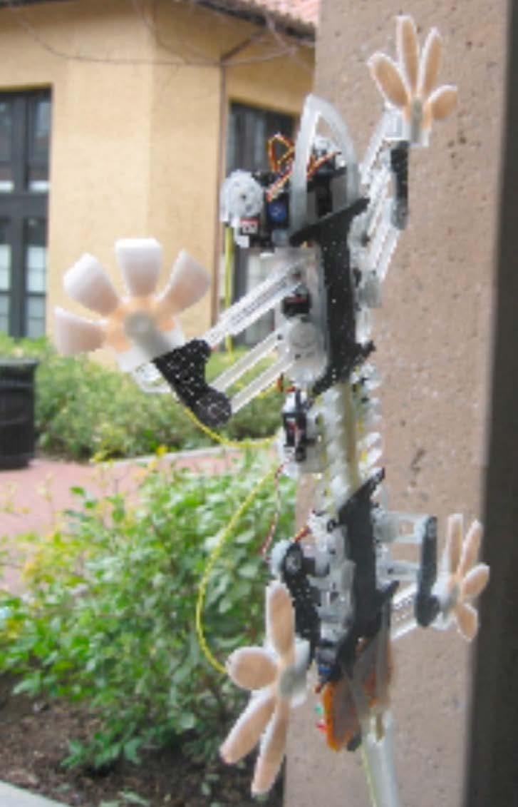
35 Adhesive Force of Gecko Toes Ben Chui, Yiching Liang and Professor Thomas Kenny, Stanford A dual-axis piezoresistive cantilever was used to characterize the adhesive properties of a single gecko seta. Studies of adhesive force under both hydrophobic and hydrophilic conditions indicate the gecko s ability to stick to and climb smooth surfaces is due to (relatively weak) van der Waals intermolecular interactions. Nanofabricated, synthetic setae show similar adhesive forces.
36
37 Nanotechnology Social and Ethical Issues Along with many potential benefits of nanotechnology, there come some possible adverse consequences and other important issues Environmental and health dangers Privacy and personal freedom issues Intellectual property and information concerns Work force and sociology effects Misleading claims, and even falsified data Others..
38 Nanotechnology Nanotechnology holds a lot of promise in terms of potential applications and products. Whatever the exact definition, key features in this field are: combining different sciences and technologies enhanced or new properties new applications all at very small dimensions. And we now have sophisticated tools to build, characterize and utilize structures at the nanoscale, across a breadth of disciplines. But we must also be aware of possible consequences.
Nanotechnology. Gavin Lawes Department of Physics and Astronomy
 Nanotechnology Gavin Lawes Department of Physics and Astronomy Earth-Moon distance 4x10 8 m (courtesy NASA) Length scales (Part I) Person 2m Magnetic nanoparticle 5x10⁻⁹ m 10 10 m 10 5 m 1 m 10-5 m 10-10
PV Tutorial Allen Hermann, Ph. D. Professor of Physics Emeritus, and Professor of Music Adjunct, University of Colorado, Boulder, Colorado, USA and
 PV Tutorial Allen Hermann, Ph. D. Professor of Physics Emeritus, and Professor of Music Adjunct, University of Colorado, Boulder, Colorado, USA and Vice-president, NanoTech Inc. Lexington, Kentucky, USA
672 Advanced Solid State Physics. Scanning Tunneling Microscopy
 672 Advanced Solid State Physics Scanning Tunneling Microscopy Biao Hu Outline: 1. Introduction to STM 2. STM principle & working modes 3. STM application & extension 4. STM in our group 1. Introduction
Nanotechnology where size matters
 Nanotechnology where size matters J Emyr Macdonald Overview Ways of seeing very small things What is nanotechnology and why is it important? Building nanostructures What we can do with nanotechnology?
Kavli Workshop for Journalists. June 13th, CNF Cleanroom Activities
 Kavli Workshop for Journalists June 13th, 2007 CNF Cleanroom Activities Seeing nm-sized Objects with an SEM Lab experience: Scanning Electron Microscopy Equipment: Zeiss Supra 55VP Scanning electron microscopes
29: Nanotechnology. What is Nanotechnology? Properties Control and Understanding. Nanomaterials
 29: Nanotechnology What is Nanotechnology? Properties Control and Understanding Nanomaterials Making nanomaterials Seeing at the nanoscale Quantum Dots Carbon Nanotubes Biology at the Nanoscale Some Applications
Nanotechnology Fabrication Methods.
 Nanotechnology Fabrication Methods. 10 / 05 / 2016 1 Summary: 1.Introduction to Nanotechnology:...3 2.Nanotechnology Fabrication Methods:...5 2.1.Top-down Methods:...7 2.2.Bottom-up Methods:...16 3.Conclusions:...19
Nanotechnology. Yung Liou P601 Institute of Physics Academia Sinica
 Nanotechnology Yung Liou P601 yung@phys.sinica.edu.tw Institute of Physics Academia Sinica 1 1st week Definition of Nanotechnology The Interagency Subcommittee on Nanoscale Science, Engineering and Technology
Nanotechnology Nanofabrication of Functional Materials. Marin Alexe Max Planck Institute of Microstructure Physics, Halle - Germany
 Nanotechnology Nanofabrication of Functional Materials Marin Alexe Max Planck Institute of Microstructure Physics, Halle - Germany Contents Part I History and background to nanotechnology Nanoworld Nanoelectronics
Nanotechnology? Source: National Science Foundation (NSF), USA
, USA") 2 2 Nanotechnology? Ability to work at the atomic, molecular and even sub-molecular levels in order to create and use material structures, devices and systems with new properties and functions Source:
2 2 Nanotechnology? Ability to work at the atomic, molecular and even sub-molecular levels in order to create and use material structures, devices and systems with new properties and functions Source:
Image courtesy of Dr James Bendall, University of Cambridge, UK. Discover the secrets h of the Nanoworld
 Image courtesy of Dr James Bendall, University of Cambridge, UK. Discover the secrets h of the Nanoworld Nano has become a buzz word in popular culture to just mean small. To understand nanotechnology
Nanotechnology: Today and tomorrow
 Nanotechnology: Today and tomorrow Horst-Günter Rubahn NanoSYD Mads Clausen Instituttet Syddansk Universitet Alsion 2 6400 Sønderborg Agenda Alsion A bit about nano Nanoproducts Top down vs. bottom up
NANOTECHNOLOGY. Students will gain an understanding of nanoscale dimensions and nanotechnology.
 NANOTECHNOLOGY By Anna M. Waldron and Carl A. Batt, Nanobiotechnology Center, Cornell University Subjects: Nanotechnology, Chemistry, Physics Time: Two class periods (approximately 90 minutes) Objective:
Final Reading Assignment: Travels to the Nanoworld: pages pages pages
 Final Reading Assignment: Travels to the Nanoworld: pages 152-164 pages 201-214 pages 219-227 Bottom-up nanofabrication Can we assemble nanomachines manually? What are the components (parts)? nanoparticles
In the name of Allah
 In the name of Allah Nano chemistry- 4 th stage Lecture No. 1 History of nanotechnology 16-10-2016 Assistance prof. Dr. Luma Majeed Ahmed lumamajeed2013@gmail.com, luma.ahmed@uokerbala.edu.iq Nano chemistry-4
There s plenty of room at the bottom! - R.P. Feynman, Nanostructure: a piece of material with at least one dimension less than 100 nm in extent.
 Nanostructures and Nanotechnology There s plenty of room at the bottom! - R.P. Feynman, 1959 Materials behave differently when structured at the nm scale than they do in bulk. Technologies now exist that
There's Plenty of Room at the Bottom
 There's Plenty of Room at the Bottom 12/29/1959 Feynman asked why not put the entire Encyclopedia Britannica (24 volumes) on a pin head (requires atomic scale recording). He proposed to use electron microscope
Understanding the properties and behavior of groups of interacting atoms more than simple molecules
 Condensed Matter Physics Scratching the Surface Understanding the properties and behavior of groups of interacting atoms more than simple molecules Solids and fluids in ordinary and exotic states low energy
MSN551 LITHOGRAPHY II
 MSN551 Introduction to Micro and Nano Fabrication LITHOGRAPHY II E-Beam, Focused Ion Beam and Soft Lithography Why need electron beam lithography? Smaller features are required By electronics industry:
Introduction to Nanoscience and Nanotechnology
 Introduction to Nanoscience and Nanotechnology ENS 463 by Alexander M. Zaitsev alexander.zaitsev@csi.cuny.edu Tel: 718 982 2812 Office 4N101b 1 What is the size for a nano? 10-3 m, (milli) Macroobjects,
Seminars in Nanosystems - I
 Seminars in Nanosystems - I Winter Semester 2011/2012 Dr. Emanuela Margapoti Emanuela.Margapoti@wsi.tum.de Dr. Gregor Koblmüller Gregor.Koblmueller@wsi.tum.de Seminar Room at ZNN 1 floor Topics of the
ME 4875/MTE C/18. Introduction to Nanomaterials and Nanotechnology. Lecture 1 - Introduction
 ME 4875/MTE 575 - C/18 Introduction to Nanomaterials and Nanotechnology Lecture 1 - Introduction 1 Course Information Syllabus uploaded to Canvas Schedule: Lectures MT-RF 10:00-10:50 pm in Olin Hall 223
Scanning Tunneling Microscopy
 Scanning Tunneling Microscopy References: 1. G. Binnig, H. Rohrer, C. Gerber, and Weibel, Phys. Rev. Lett. 49, 57 (1982); and ibid 50, 120 (1983). 2. J. Chen, Introduction to Scanning Tunneling Microscopy,
Nanoscale Issues in Materials & Manufacturing
 Nanoscale Issues in Materials & Manufacturing ENGR 213 Principles of Materials Engineering Module 2: Introduction to Nanoscale Issues Top-down and Bottom-up Approaches for Fabrication Winfried Teizer,
ME 4875/MTE C/16. Introduction to Nanomaterials and Nanotechnology. Lecture 1 - Introduction
 ME 4875/MTE 575 - C/16 Introduction to Nanomaterials and Nanotechnology Lecture 1 - Introduction 1 Course Information Syllabus uploaded to mywpi Schedule: Lectures MT-RF 2:00-2:50 pm in Salisbury Labs
National Science and Technology Council (NSTC) Committee on Technology
 Committee on Technology") BY LYNN YARRIS "The emerging fields of nanoscience and nanoengineering are leading to unprecedented understanding and control over the fundamental building blocks of all physical things. This is likely
BY LYNN YARRIS "The emerging fields of nanoscience and nanoengineering are leading to unprecedented understanding and control over the fundamental building blocks of all physical things. This is likely
Jeopardy Q $100 Q $100 Q $100 Q $100 Q $100 Q $200 Q $200 Q $200 Q $200 Q $200 Q $300 Q $300 Q $300 Q $300 Q $300 Q $400 Q $400 Q $400 Q $400 Q $400
 Jeopardy Size and Scale Nano Products Tools Structure Of Matter Science and Society Q $100 Q $200 Q $300 Q $400 Q $500 Q $100 Q $100 Q $100 Q $100 Q $200 Q $200 Q $200 Q $200 Q $300 Q $300 Q $300 Q $300
Nanostructure. Materials Growth Characterization Fabrication. More see Waser, chapter 2
 Nanostructure Materials Growth Characterization Fabrication More see Waser, chapter 2 Materials growth - deposition deposition gas solid Physical Vapor Deposition Chemical Vapor Deposition Physical Vapor
Like space travel and the Internet before it, the possibilities of the nano world catches the imagination of school children and scientists alike.
 The Nano World Preface Nano is the cool thing and it s the buzzword Like space travel and the Internet before it, the possibilities of the nano world catches the imagination of school children and scientists
Nanotubes and Nanowires - One-dimensional Materials
 NCLT July 13th, 2006 Nanotubes and Nanowires - One-dimensional Materials Tim Sands Materials Engineering and Electrical & Computer Engineering Birck Nanotechnology Center Purdue University 100 nm Si/SiGe
Lesson 4: Tools of the Nanosciences. Student Materials
 Lesson 4: Tools of the Nanosciences Student Materials Contents Black Box Lab Activity: Student Instructions and Worksheet Seeing and Building Small Things: Student Reading Seeing and Building Small Things:
Chapter 10. Nanometrology. Oxford University Press All rights reserved.
 Chapter 10 Nanometrology Oxford University Press 2013. All rights reserved. 1 Introduction Nanometrology is the science of measurement at the nanoscale level. Figure illustrates where nanoscale stands
Dr. PUJA CHAWLA. * - ASSISTANT PROFESSOR (PHYSICS) JMIT, RADAUR, HARYANA, INDIA.
 JMIT, RADAUR, HARYANA, INDIA.") Dr. PUJA CHAWLA *E-mail- dr.poojachawla@jmit.ac.in ASSISTANT PROFESSOR (PHYSICS) JMIT, RADAUR, HARYANA, INDIA. NANOTECHNOLOGY & NANOMATERIALS Introduction Nanotechnology & Nanomaterials Synthesis of nanomaterials:
Dr. PUJA CHAWLA *E-mail- dr.poojachawla@jmit.ac.in ASSISTANT PROFESSOR (PHYSICS) JMIT, RADAUR, HARYANA, INDIA. NANOTECHNOLOGY & NANOMATERIALS Introduction Nanotechnology & Nanomaterials Synthesis of nanomaterials:
Institute for Electron Microscopy and Nanoanalysis Graz Centre for Electron Microscopy
 Institute for Electron Microscopy and Nanoanalysis Graz Centre for Electron Microscopy Micromechanics Ass.Prof. Priv.-Doz. DI Dr. Harald Plank a,b a Institute of Electron Microscopy and Nanoanalysis, Graz
WJEC England GCSE Chemistry. Topic 5: Bonding, structure and properties. Notes. (Content in bold is for Higher Tier only)
") WJEC England GCSE Chemistry Topic 5: Bonding, structure and properties Notes (Content in bold is for Higher Tier only) Chemical bonds Compounds - substances in which 2 or more elements are chemically combined.
WJEC England GCSE Chemistry Topic 5: Bonding, structure and properties Notes (Content in bold is for Higher Tier only) Chemical bonds Compounds - substances in which 2 or more elements are chemically combined.
RAJASTHAN TECHNICAL UNIVERSITY, KOTA
 RAJASTHAN TECHNICAL UNIVERSITY, KOTA (Electronics & Communication) Submitted By: LAKSHIKA SOMANI E&C II yr, IV sem. Session: 2007-08 Department of Electronics & Communication Geetanjali Institute of Technical
Computers of the Future? Moore s Law Ending in 2018?
 Computers of the Future? CS 221 Moore s Law Ending in 2018? Moore s Law: Processor speed / number transistors doubling approximately 18 months 1 Moore s Law Moore s Law Recent research predicts an end
Nanostrukturphysik (Nanostructure Physics)
") Nanostrukturphysik (Nanostructure Physics) Prof. Yong Lei & Dr. Yang Xu Fachgebiet 3D-Nanostrukturierung, Institut für Physik Contact: yong.lei@tu-ilmenau.de; yang.xu@tu-ilmenau.de Office: Unterpoerlitzer
Nanostrukturphysik (Nanostructure Physics) Prof. Yong Lei & Dr. Yang Xu Fachgebiet 3D-Nanostrukturierung, Institut für Physik Contact: yong.lei@tu-ilmenau.de; yang.xu@tu-ilmenau.de Office: Unterpoerlitzer
Contents. What is AFM? History Basic principles and devices Operating modes Application areas Advantages and disadvantages
 Contents What is AFM? History Basic principles and devices Operating modes Application areas Advantages and disadvantages Figure1: 2004 Seth Copen Goldstein What is AFM? A type of Scanning Probe Microscopy
General concept and defining characteristics of AFM. Dina Kudasheva Advisor: Prof. Mary K. Cowman
 General concept and defining characteristics of AFM Dina Kudasheva Advisor: Prof. Mary K. Cowman Overview Introduction History of the SPM invention Technical Capabilities Principles of operation Examples
ME 4875/MTE C16. Introduction to Nanomaterials and Nanotechnology. Lecture 2 - Applications of Nanomaterials + Projects
 ME 4875/MTE 575 - C16 Introduction to Nanomaterials and Nanotechnology Lecture 2 - Applications of Nanomaterials + Projects 1 Project Teams of 4 students each Literature review of one application of nanotechnology
Graphene The Search For Two Dimensions. Christopher Scott Friedline Arizona State University
 Graphene The Search For Two Dimensions Christopher Scott Friedline Arizona State University What Is Graphene? Single atomic layer of graphite arranged in a honeycomb crystal lattice Consists of sp 2 -bonded
LECTURE 1 : INTRODUCTION TO NANOMECHANICS
 I LECTURE 1 : INTRODUCTION TO NANOMECHANICS Outline : NANOTECHNOLOGY / NANOMECHANICS DEFINITIONS... 2 WHY IS NANO INTERESTING?... 3 HISTORY OF NANOTECHNOLOGY/NANOMECHANICS : TIME LINE... 4 The First Talk
Nanostructures Fabrication Methods
 Nanostructures Fabrication Methods bottom-up methods ( atom by atom ) In the bottom-up approach, atoms, molecules and even nanoparticles themselves can be used as the building blocks for the creation of
L8: The Mechanics of Adhesion used by the Gecko
 L8: The Mechanics of Adhesion used by the Gecko With help from Bo He Overview Gecko s foot structure Intermolecular force Measurement: 2-D MEMS sensor Gecko s adhesive mechanism Measurement results discussion
CSCI 2570 Introduction to Nanocomputing
 CSCI 2570 Introduction to Nanocomputing The Emergence of Nanotechnology John E Savage Purpose of the Course The end of Moore s Law is in sight. Researchers are now exploring replacements for standard methods
NANOMEDICINE. WILEY A John Wiley and Sons, Ltd., Publication DESIGN AND APPLICATIONS OF MAGNETIC NANOMATERIALS, NANOSENSORS AND NANOSYSTEMS
 NANOMEDICINE DESIGN AND APPLICATIONS OF MAGNETIC NANOMATERIALS, NANOSENSORS AND NANOSYSTEMS Vijay K. Varadan Linfeng Chen Jining Xie WILEY A John Wiley and Sons, Ltd., Publication Preface About the Authors
The Dielectric Function of a Metal ( Jellium )
") The Dielectric Function of a Metal ( Jellium ) Total reflection Plasma frequency p (10 15 Hz range) Why are Metals Shiny? An electric field cannot exist inside a metal, because metal electrons follow the
The Dielectric Function of a Metal ( Jellium ) Total reflection Plasma frequency p (10 15 Hz range) Why are Metals Shiny? An electric field cannot exist inside a metal, because metal electrons follow the
Simple piezoresistive accelerometer
 Simple piezoresistive pressure sensor Simple piezoresistive accelerometer Simple capacitive accelerometer Cap wafer C(x)=C(x(a)) Cap wafer may be micromachined silicon, pyrex, Serves as over-range protection,
Electrochemically Synthesized Multi-block
 Electrochemically Synthesized Multi-block Nanorods Sungho Park SungKyunKwan University, Department of Chemistry & SKKU Advanced Institute of Nanotechnology (SAINT) J. Am. Chem. Soc. 2003, 125, 2282-2290
Nano-mechatronics. Presented by: György BudaváriSzabó (X0LY4M)
") Nano-mechatronics Presented by: György BudaváriSzabó (X0LY4M) Nano-mechatronics Nano-mechatronics is currently used in broader spectra, ranging from basic applications in robotics, actuators, sensors,
Nano-mechatronics Presented by: György BudaváriSzabó (X0LY4M) Nano-mechatronics Nano-mechatronics is currently used in broader spectra, ranging from basic applications in robotics, actuators, sensors,
Introduction to Photolithography
 http://www.ichaus.de/news/72 Introduction to Photolithography Photolithography The following slides present an outline of the process by which integrated circuits are made, of which photolithography is
MRSEC. Refrigerator Magnet Activity Guide. Quick Reference Activity Guide. a) b) c) = north = south. Activity Materials
 b) c) = north = south. Activity Materials") MRSEC Refrigerator Magnet Activity Guide Quick Reference Activity Guide Activity Materials Refrigerator magnet with removable probe strip Magnetic field diagrams Starting Points One of the great breakthroughs
MRSEC Refrigerator Magnet Activity Guide Quick Reference Activity Guide Activity Materials Refrigerator magnet with removable probe strip Magnetic field diagrams Starting Points One of the great breakthroughs
Nanobiotechnology. Place: IOP 1 st Meeting Room Time: 9:30-12:00. Reference: Review Papers. Grade: 40% midterm, 60% final report (oral + written)
") Nanobiotechnology Place: IOP 1 st Meeting Room Time: 9:30-12:00 Reference: Review Papers Grade: 40% midterm, 60% final report (oral + written) Midterm: 5/18 Oral Presentation 1. 20 minutes each person
Nanobiotechnology Place: IOP 1 st Meeting Room Time: 9:30-12:00 Reference: Review Papers Grade: 40% midterm, 60% final report (oral + written) Midterm: 5/18 Oral Presentation 1. 20 minutes each person
materials, devices and systems through manipulation of matter at nanometer scale and exploitation of novel phenomena which arise because of the
 Nanotechnology is the creation of USEFUL/FUNCTIONAL materials, devices and systems through manipulation of matter at nanometer scale and exploitation of novel phenomena which arise because of the nanometer
MEEN Nanoscale Issues in Manufacturing. Lithography Lecture 1: The Lithographic Process
 MEEN 489-500 Nanoscale Issues in Manufacturing Lithography Lecture 1: The Lithographic Process 1 Discuss Reading Assignment 1 1 Introducing Nano 2 2 Size Matters 3 3 Interlude One-The Fundamental Science
Far IR Gas Lasers microns wavelengths, THz frequency Called Terahertz lasers or FIR lasers At this wavelength behaves more like
 Far IR Gas Lasers 10-1500 microns wavelengths, 300 10 THz frequency Called Terahertz lasers or FIR lasers At this wavelength behaves more like microwave signal than light Created by Molecular vibronic
Nanotechnology. An Introduction
 Nanotechnology An Introduction Nanotechnology A new interdisciplinary field of science The study of systems at the nanoscale The use of tools at the nanoscale Building and applying structures that are
ESH Benign Processes for he Integration of Quantum Dots (QDs)
") ESH Benign Processes for he Integration of Quantum Dots (QDs) PIs: Karen K. Gleason, Department of Chemical Engineering, MIT Graduate Students: Chia-Hua Lee: PhD Candidate, Department of Material Science
ESH Benign Processes for he Integration of Quantum Dots (QDs) PIs: Karen K. Gleason, Department of Chemical Engineering, MIT Graduate Students: Chia-Hua Lee: PhD Candidate, Department of Material Science
Techniken der Oberflächenphysik (Techniques of Surface Physics)
") Techniken der Oberflächenphysik (Techniques of Surface Physics) Prof. Yong Lei & Dr. Yang Xu (& Liying Liang) Fachgebiet 3D-Nanostrukturierung, Institut für Physik Contact: yong.lei@tu-ilmenau.de; yang.xu@tu-ilmenau.de;
Techniken der Oberflächenphysik (Techniques of Surface Physics) Prof. Yong Lei & Dr. Yang Xu (& Liying Liang) Fachgebiet 3D-Nanostrukturierung, Institut für Physik Contact: yong.lei@tu-ilmenau.de; yang.xu@tu-ilmenau.de;
bio-molecular studies Physical methods in Semmelweis University Osváth Szabolcs
 Physical methods in bio-molecular studies Osváth Szabolcs Semmelweis University szabolcs.osvath@eok.sote.hu Light emission and absorption spectra Stokes shift is the difference (in wavelength or frequency
Imaging Carbon materials with correlative Raman-SEM microscopy. Introduction. Raman, SEM and FIB within one chamber. Diamond.
 Imaging Carbon materials with correlative Raman-SEM microscopy Application Example Carbon materials are widely used in many industries for their exceptional properties. Electric conductance, light weight,
In today s lecture, we will cover:
 In today s lecture, we will cover: Metal and Metal oxide Nanoparticles Semiconductor Nanocrystals Carbon Nanotubes 1 Week 2: Nanoparticles Goals for this section Develop an understanding of the physical
Fabrication at the nanoscale for nanophotonics
 Fabrication at the nanoscale for nanophotonics Ilya Sychugov, KTH Materials Physics, Kista silicon nanocrystal by electron beam induced deposition lithography Outline of basic nanofabrication methods Devices
Molecular Electronics For Fun and Profit(?)
") Molecular Electronics For Fun and Profit(?) Prof. Geoffrey Hutchison Department of Chemistry University of Pittsburgh geoffh@pitt.edu July 22, 2009 http://hutchison.chem.pitt.edu Moore s Law: Transistor
Molecular Electronics For Fun and Profit(?) Prof. Geoffrey Hutchison Department of Chemistry University of Pittsburgh geoffh@pitt.edu July 22, 2009 http://hutchison.chem.pitt.edu Moore s Law: Transistor
2.76/2.760 Multiscale Systems Design & Manufacturing
 2.76/2.760 Multiscale Systems Design & Manufacturing Fall 2004 MOEMS Devices for Optical communications system Switches and micromirror for Add/drops Diagrams removed for copyright reasons. MOEMS MEMS
MEMS Metrology. Prof. Tianhong Cui ME 8254
 MEMS Metrology Prof. Tianhong Cui ME 8254 What is metrology? Metrology It is the science of weights and measures Refers primarily to the measurements of length, weight, time, etc. Mensuration- A branch
I. NANOFABRICATION O AND CHARACTERIZATION Chap. 2 : Self-Assembly
 I. Nanofabrication and Characterization : TOC I. NANOFABRICATION O AND CHARACTERIZATION Chap. 1 : Nanolithography Chap. 2 : Self-Assembly Chap. 3 : Scanning Probe Microscopy Nanoscale fabrication requirements
Picotechnology refers to the structuring of matter on a true picometer scale.
 Picotechnology It is a level of technological manipulation of matter on the scale of trillionths of a meter or picoscale (10 12 ). This is one order of magnitude smaller than a nanometer and one order
Basic Laboratory. Materials Science and Engineering. Atomic Force Microscopy (AFM)
") Basic Laboratory Materials Science and Engineering Atomic Force Microscopy (AFM) M108 Stand: 20.10.2015 Aim: Presentation of an application of the AFM for studying surface morphology. Inhalt 1.Introduction...
Basic Laboratory Materials Science and Engineering Atomic Force Microscopy (AFM) M108 Stand: 20.10.2015 Aim: Presentation of an application of the AFM for studying surface morphology. Inhalt 1.Introduction...
PHY313 - CEI544 The Mystery of Matter From Quarks to the Cosmos Fall 2005
 PHY313 - CEI544 The Mystery of Matter From Quarks to the Cosmos Fall 2005 Peter Paul Office Physics D-143 www.physics.sunysb.edu then click on PHY313 or CEI544 Peter Paul 09/1/05 PHY313-CEI544 Fall-05
Nanosphere Lithography
 Nanosphere Lithography Derec Ciafre 1, Lingyun Miao 2, and Keita Oka 1 1 Institute of Optics / 2 ECE Dept. University of Rochester Abstract Nanosphere Lithography is quickly emerging as an efficient, low
Overview of Nanotechnology Applications and Relevant Intellectual Property NANO POWER PATENTS
 Overview of Nanotechnology Applications and Relevant Intellectual Property NANO POWER PATENTS Jeffrey H. Rosedale, Ph.D., J.D. Registered Patent Attorney Partner, Woodcock Washburn, LLP ~ 9000 Issued U.S.
Chapter 12. Nanometrology. Oxford University Press All rights reserved.
 Chapter 12 Nanometrology Introduction Nanometrology is the science of measurement at the nanoscale level. Figure illustrates where nanoscale stands in relation to a meter and sub divisions of meter. Nanometrology
From Last Time. Mon. Nov 8 Phy107 Lecture 26
 From Last Time Particle can exist in different quantum states, having Different energy Different momentum Different wavelength The quantum wavefunction describes wave nature of particle. Square of the
Nanophysics: Main trends
 Nano-opto-electronics Nanophysics: Main trends Nanomechanics Main issues Light interaction with small structures Molecules Nanoparticles (semiconductor and metallic) Microparticles Photonic crystals Nanoplasmonics
Materials. Definitions of nanotechnology. The term nanotechnology was invented by Professor Norio Taniguchi at the University of Tokyo in 1971.
 Materials Definitions of nanotechnology The term nanotechnology was invented by Professor Norio Taniguchi at the University of Tokyo in 1971. The original definition, translated into English Nano-technology'
Microfabrication for MEMS: Part I
 Microfabrication for MEMS: Part I Carol Livermore Massachusetts Institute of Technology * With thanks to Steve Senturia, from whose lecture notes some of these materials are adapted. CL: 6.777J/2.372J
CORE MOLIT ACTIVITIES at a glance
 CORE MOLIT ACTIVITIES at a glance 1. Amplification of Biochemical Signals: The ELISA Test http://molit.concord.org/database/activities/248.html The shape of molecules affects the way they function. A test
Contents. Preface to the first edition
 Contents List of authors Preface to the first edition Introduction x xi xiii 1 The nanotechnology revolution 1 1.1 From micro- to nanoelectronics 2 1.2 From the macroscopic to the nanoscopic world 4 1.3
Micro/nano and precision manufacturing technologies and applications
 The 4th China-American Frontiers of Engineering Symposium Micro/nano and precision manufacturing technologies and applications Dazhi Wang School of Mechanical Engineering Dalian University of Technology
1.1. Introduction to Nanoscience and Nanotechnology
 1.1. Introduction to Nanoscience and Nanotechnology 1.1.1. A Brief Historical Overview Before trying to understand and discuss about synthesis, characterization and application of nanomaterials, it is
Overview of the main nano-lithography techniques
 Overview of the main nano-lithography techniques Soraya Sangiao sangiao@unizar.es Outline Introduction: Nanotechnology. Nano-lithography techniques: Masked lithography techniques: Photolithography. X-ray
The design of an integrated XPS/Raman spectroscopy instrument for co-incident analysis
 The design of an integrated XPS/Raman spectroscopy instrument for co-incident analysis Tim Nunney The world leader in serving science 2 XPS Surface Analysis XPS +... UV Photoelectron Spectroscopy UPS He(I)
From nanophysics research labs to cell phones. Dr. András Halbritter Department of Physics associate professor
 From nanophysics research labs to cell phones Dr. András Halbritter Department of Physics associate professor Curriculum Vitae Birth: 1976. High-school graduation: 1994. Master degree: 1999. PhD: 2003.
AFM Imaging In Liquids. W. Travis Johnson PhD Agilent Technologies Nanomeasurements Division
 AFM Imaging In Liquids W. Travis Johnson PhD Agilent Technologies Nanomeasurements Division Imaging Techniques: Scales Proteins 10 nm Bacteria 1μm Red Blood Cell 5μm Human Hair 75μm Si Atom Spacing 0.4nm
Chapter 6 Magnetic nanoparticles
 Chapter 6 Magnetic nanoparticles Magnetic nanoparticles (MNPs) are a class of nanoparticle which can be manipulated using magnetic field gradients. Such particles commonly consist of magnetic elements
Integrating MEMS Electro-Static Driven Micro-Probe and Laser Doppler Vibrometer for Non-Contact Vibration Mode SPM System Design
 Tamkang Journal of Science and Engineering, Vol. 12, No. 4, pp. 399 407 (2009) 399 Integrating MEMS Electro-Static Driven Micro-Probe and Laser Doppler Vibrometer for Non-Contact Vibration Mode SPM System
How do scientists build something so small? Materials 1 pkg of modeling materials 1 piece of butcher paper 1 set of cards 1 set of markers
 Using Modeling to Demonstrate Self-Assembly in Nanotechnology Imagine building a device that is small enough to fit on a contact lens. It has an antennae and a translucent screen across the pupil of the
Figure 1: Some examples of objects at different size scales ( 2001, CMP Científica, [2])
![Figure 1: Some examples of objects at different size scales ( 2001, CMP Científica, [2])](/thumbs/85/91872790.jpg "Figure 1: Some examples of objects at different size scales ( 2001, CMP Científica, [2])") Top-Down vs. Bottom-Up Nanomanufacturing Prof. Derek J. Hansford, Biomedical Engineering Program and Department of Materials Science & Engineering Learning Objectives: This module should expose the student
Top-Down vs. Bottom-Up Nanomanufacturing Prof. Derek J. Hansford, Biomedical Engineering Program and Department of Materials Science & Engineering Learning Objectives: This module should expose the student
CHAPTER EIGHT: PHOTONIC CRYSTALS: MATERIALS, END USES, AND MARKETS, MATERIALS PROPERTIES... 78
 CHAPTER ONE: INTRODUCTION... 1 STUDY BACKGROUND... 1 STUDY GOALS AND OBJECTIVES... 1 INTENDED AUDIENCE... 2 SCOPE AND FORMAT... 2 INFORMATION SOURCES AND METHODOLOGY... 3 ANALYST CREDENTIALS... 4 RELATED
EE C245 ME C218 Introduction to MEMS Design Fall 2007
 EE C245 ME C218 Introduction to MEMS Design Fall 2007 Prof. Clark T.-C. Nguyen Dept. of Electrical Engineering & Computer Sciences University of California at Berkeley Berkeley, CA 94720 Lecture 12: Mechanics
Lesson 1: Introduction to Nanoscience. Teacher Materials
 Lesson 1: Introduction to Nanoscience Teacher Materials Contents Introduction to Nanoscience: Teacher Lesson Plan Introduction to Nanoscience: PowerPoint with Teacher Notes Introduction to Nanoscience
Title Single Row Nano-Tribological Printing: A novel additive manufacturing method for nanostructures
 Nano-Tribological Printing: A novel additive manufacturing method for nanostructures H.S. Khare, N.N. Gosvami, I. Lahouij, R.W. Carpick hkhare@seas.upenn.edu carpick@seas.upenn.edu carpick.seas.upenn.edu
Nanomechanics Measurements and Standards at NIST
 Nanomechanics Measurements and Standards at NIST Robert F. Cook Deputy Chief, Ceramics Division Leader, Nanomechanical Properties Group robert.cook@nist.gov NIST Mission Promote U.S. innovation and industrial
Scanning Probe Microscopy (SPM)
") http://ww2.sljus.lu.se/staff/rainer/spm.htm Scanning Probe Microscopy (FYST42 / FAFN30) Scanning Probe Microscopy (SPM) overview & general principles March 23 th, 2018 Jan Knudsen, room K522, jan.knudsen@sljus.lu.se
http://ww2.sljus.lu.se/staff/rainer/spm.htm Scanning Probe Microscopy (FYST42 / FAFN30) Scanning Probe Microscopy (SPM) overview & general principles March 23 th, 2018 Jan Knudsen, room K522, jan.knudsen@sljus.lu.se
0 volts. 2 volts. 5 volts
 CS101 Binary Storage Devices and Boolean Logic Now that we have discussed number representation, why do computers use the binary representation and not something we are more familiar with, like decimal?
NANOCOMPOSITE THIN FILMS:
 NANOCOMPOSITE THIN FILMS: Assembly, Characterizations, & Applications Chaoyang Jiang Department of Chemistry The University of South Dakota St. Louis, June 26, 2008 Forest Products &Nanocomposite P. Monteiro@UC
Laser and Plasma-based Nanotechnologies
 Simpozionul: De la excelenta la competitivitate: tehnologiile generice esentiale Aula Academiei Romane, Bucuresti 15 mai 2014. Laser and Plasma-based Nanotechnologies Marian ZAMFIRESCU National Institute
Wafer-scale fabrication of graphene
 Wafer-scale fabrication of graphene Sten Vollebregt, MSc Delft University of Technology, Delft Institute of Mircosystems and Nanotechnology Delft University of Technology Challenge the future Delft University