Image courtesy of Dr James Bendall, University of Cambridge, UK. Discover the secrets h of the Nanoworld
|
|
|
- Roland Washington
- 5 years ago
- Views:
Transcription

1 Image courtesy of Dr James Bendall, University of Cambridge, UK. Discover the secrets h of the Nanoworld

2 Nano has become a buzz word in popular culture to just mean small.
3 To understand nanotechnology we must first think about scale.

4 A nanometre is the unit of measurement used in the nanoscale.


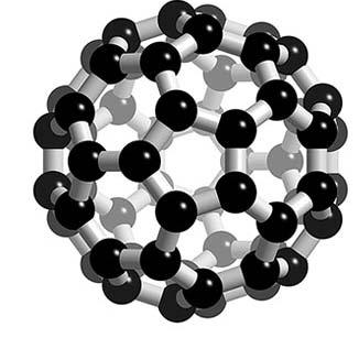
5 Quite a few nanometres here! C 60 is a nanoparticle as its diameter is just over 1 nm

6


7 Dog 10 0 m or 1,000,000,000 nm in length. Flea 10-3 m or 1,000,000 nm in length Red Blood cells 10-5 m or 6000 nm in diameter DNA 10-8 m or 2.5nm in diameter. Nanoparticle 10-9 m. One dimension between 1 and 100 nm.
8 A water molecule which measures approximately 0.5 nm is about as big in relation to an apple as an apple is to planet Earth. It s a long way down to the nanoscale!


9 Nanoparticles are just tiny bits of a larger material but what happens when you create such small pieces? Images of gold nanoparticles courtsey of Paul Rhatigan, Cambridge University.
10 Tiny pieces = more.
11 1cm Surface Area 1cm 4cm 2cm 6cm 2 3cm 12cm 2 3cm
12

13 Nanoparticles have more surface area. This makes them more reactive since chemical reactions happen on the surface. More reactive means potentially more useful.


14 In a cubic centimetre of material one in 10 million atoms are on the surface but for a cubic nanometre, 80% of atoms are on the surface and potentially ready to react! Images courtesy of Dr Colm Durkan, Cambridge University.

15 Size is the key here! At the Nanoscale a material s properties can change dramatically. These could be their boiling points, solubility or catalytic activity. With only a reduction in size materials can exhibit new properties, properties they do not possess when they are on a larger or macro scale. The normal classical laws of physics no longer apply!


16 Colour changes For example, sometimes just changing the size of a particle can drastically alter its colour. Cadmium Telluride MACRO Gold MACRO Increasing size Nanoparticles of CdTe. A. Eychmüller, Technische Universität Dresden


17 Even mechanical and electrical properties can be influenced by size! Graphene is brittle and nonconductive Carbon nanotubes are like graphene sheets but rolled up however they have totally different properties. Did you know? Carbon nanotubes are much stronger than steel yet much lighter, and they can be conductive.

18 So how do scientists work on such a tiny scale?
19


20 Mainly because microscopes have become more sophisticated. Micrographia The first microscopes to be developed in around 1665 opened up a whole new world for scientists. For the first time cells and structures of nature that we are familiar with now became visible. Public opinion was fearful of this voyage into the unseen world of the microscopic.


21 Now we have microscopes that can see even further into this world, actually to the atoms that are the very building blocks of our living world. These more sophisticated microscopes are known collectively as Scanning Probe Microscopes or SPMs.

22 A Scanning Probe Microscope uses an extremely fine probe tip (sometimes ending in only a few atoms) and runs over the surface feeling for contours and shapes. Probe tip feeling for shapes. Examples include: Atomic Force Microscope, Scanning Tunnelling Microscope


23 A cantilever, similar to a diving board, is attached to the tip of an Atomic Force Microscope or AFM. The whole thing moves up and down as the tip moves over the atomic scale hills and valleys of a sample s surface. detector computer Laser Probe tip Sample This is a diagram of an Atomic Force Microscope, or AFM A laser reflects off the back of the cantilever. When the cantilever deflects, so does the laser beam. A detector in a computer records the movement of the laser and translates that data into an image, such as the images on the right. Images courtesy of T. Oppenheim, Cambridge University


24 Scanning tunnelling microscope. A scanning tunnelling microscope works by having a tiny probe which scans across a surface picking up variations in the current that runs between itself and the atoms on the surface. This probe is made of conducting material (usually Tungsten) and the very end of it is only 1 atom wide! These variations in current are translated into images such as the ones to the right. A tungsten tip for STM imaging. Images courtesy of Cambridge university, Nanoscience Centre.

25 The probe tips can also be used to move individual atoms. Image originally created by Don Eigler, IBM corporation. The image shows iron atoms which have been moved individually.

26


27 This idea of building things from the atoms and working up is interesting for researchers. BOTTOM UP TOP DOWN Computers and phones are getting smaller yet more powerful. This trend demands smaller and smaller components, getting down to the nanoscale. It makes sense to be able to create these nano-devices from the bottom up. Rather than the more traditional top down approach to manufacturing. Manufacturing from the bottom up would mean less energy and less waste.


28 Moving atoms individually is still not a viable technique for creating nanostructures because it s too slow. However there is another process called SELF ASSEMBLY, often seen in nature, which scientists can exploit. Atoms, molecules or nanoparticles will arrange themselves into larger structures if they have the right properties and environments. This process plays a central role in the construction of DNA, cells, bones and viruses. These all self assemble without assistance.

, they use electrons instead of light, this is called E-beam lithography.")
29 Another way scientists can create nano-sized devices is a process called lithography. It is often used to make computer chips. It works in a very similar way to printing or if you were spray painting over a stencil. But lithography uses light or electrons instead of ink or paint. Photolithography uses light and structures as small as around 20 nm can be made. If scientists want to make even smaller structures (around 5 nm), they use electrons instead of light, this is called E-beam lithography. This is a finished structure created by E-beam lithography. Images courtesy of Dr Atif Aziz and Dr Colm Durkan., Cambridge University.


30 In this image each letter is made up of hundreds of nanotubes! They are stronger yet considerably lighter than steel and flexible. They can behave like metals but also semiconductors, they are great at transmitting heat and they are assembled from carbon atoms. Are an exciting discovery which could revolutionise materials of the future. Courtesy of Stephan Hoffman, Cambridge University. Even when nanotubes are fully grown, each entity is smaller than a human blood cell. With properties like this they could play a pivotal role in the development of new materials and future electronics.


31 Nature is an expert in making nanoscale structures. This is why scientists look to nature for inspiration when researching how to construct at this tiny scale.
32


33 Biomimicry Biomimicry is the term scientists copying nature. By studying Lotus leaves and their structure scientists have designed non-wetting materials and self-cleaning windows. By studying butterfly wings and their nanostructures scientists have explained how light can interact differently with surfaces. This has helped design security holograms and hair products! Butterfly wings under the microscope Even the nano structure of a Toucan s beak has offered insight into designing ultra-light aircraft components.


34 Geckos feet have nanostructures. Image credit: A.Dhinojwala, University of Akron Geckos feet are covered in tiny hair-like structures called setaes. These structures can get so close to a surface that weak sticky interactions between molecules become significant. The result is strong adhesion which is entirely due to Van der Waals forces. Scientists have been inspired by this nanostructure to create internal bandages which still adhere even in a wet environment. Image credit: C. Mathisen, FEI Company Image credit: A.Kellar, Lewis & Clark College Nature is experienced in working on the nanoscale and we can learn a lot from its success at creating natural nanotechnology.
35


36 Nanotechnology is already in our lives. Nanoelectronics has enabled the miniaturisation of electronic gadgets in daily use. Some tennis balls stay bouncy for longer thanks to a nano-structured inner layer. Socks that contain antibacterial nanoparticles of silver are supposed to keep your feet healthy and odour free. Some tennis racquets are made from a carbon-based nanocomposite making them stronger and lighter than ever before.


37 Nanotechnology is already in our lives. Some textiles are made very hydrophobic using liquid repellent nanostructures which enable them to be water and stain resistant. Cosmetics and sunscreens which contain nanoparticles can promote better protection and comfort. Sun glasses which have a nano-structured coating are easier to clean, harder to scratch, anti static,anti-misting and anti-bacterial.
38


39 Nanotechnology is a multidisciplinary subject as it incorporates many different areas of science and industry:
40


41 It is the potential of Nanotechnology that makes it so interesting. Some areas where Nanotechnology could have a dramatic impact include Medical Applications e.g. cancer therapy Information Technology e.g. faster computers Energy Solutions e.g. such as more economical fuel cells and solar cells Areas which have an impact on all our lives.
42
NANOTECHNOLOGY. Students will gain an understanding of nanoscale dimensions and nanotechnology.
 NANOTECHNOLOGY By Anna M. Waldron and Carl A. Batt, Nanobiotechnology Center, Cornell University Subjects: Nanotechnology, Chemistry, Physics Time: Two class periods (approximately 90 minutes) Objective:
Nanotechnology. Gavin Lawes Department of Physics and Astronomy
 Nanotechnology Gavin Lawes Department of Physics and Astronomy Earth-Moon distance 4x10 8 m (courtesy NASA) Length scales (Part I) Person 2m Magnetic nanoparticle 5x10⁻⁹ m 10 10 m 10 5 m 1 m 10-5 m 10-10
Nanotechnology Fabrication Methods.
 Nanotechnology Fabrication Methods. 10 / 05 / 2016 1 Summary: 1.Introduction to Nanotechnology:...3 2.Nanotechnology Fabrication Methods:...5 2.1.Top-down Methods:...7 2.2.Bottom-up Methods:...16 3.Conclusions:...19
Understanding the properties and behavior of groups of interacting atoms more than simple molecules
 Condensed Matter Physics Scratching the Surface Understanding the properties and behavior of groups of interacting atoms more than simple molecules Solids and fluids in ordinary and exotic states low energy
Discovering Nanotechnology
 Glossary Agarose Nanotechnology A polysaccharide derived from seaweed that is used for the separation of molecules in electrophoresis. A term used to describe the production and the uses of nanoparticles
Investigating Nano-Space
 Name Partners Date Visual Quantum Mechanics The Next Generation Investigating Nano-Space Goal You will apply your knowledge of tunneling to understand the operation of the scanning tunneling microscope.
29: Nanotechnology. What is Nanotechnology? Properties Control and Understanding. Nanomaterials
 29: Nanotechnology What is Nanotechnology? Properties Control and Understanding Nanomaterials Making nanomaterials Seeing at the nanoscale Quantum Dots Carbon Nanotubes Biology at the Nanoscale Some Applications
Jeopardy Q $100 Q $100 Q $100 Q $100 Q $100 Q $200 Q $200 Q $200 Q $200 Q $200 Q $300 Q $300 Q $300 Q $300 Q $300 Q $400 Q $400 Q $400 Q $400 Q $400
 Jeopardy Size and Scale Nano Products Tools Structure Of Matter Science and Society Q $100 Q $200 Q $300 Q $400 Q $500 Q $100 Q $100 Q $100 Q $100 Q $200 Q $200 Q $200 Q $200 Q $300 Q $300 Q $300 Q $300
Lesson 4: Tools of the Nanosciences. Student Materials
 Lesson 4: Tools of the Nanosciences Student Materials Contents Black Box Lab Activity: Student Instructions and Worksheet Seeing and Building Small Things: Student Reading Seeing and Building Small Things:
Final Reading Assignment: Travels to the Nanoworld: pages pages pages
 Final Reading Assignment: Travels to the Nanoworld: pages 152-164 pages 201-214 pages 219-227 Bottom-up nanofabrication Can we assemble nanomachines manually? What are the components (parts)? nanoparticles
Nanotechnology. An Introduction
 Nanotechnology An Introduction Nanotechnology A new interdisciplinary field of science The study of systems at the nanoscale The use of tools at the nanoscale Building and applying structures that are
In the name of Allah
 In the name of Allah Nano chemistry- 4 th stage Lecture No. 1 History of nanotechnology 16-10-2016 Assistance prof. Dr. Luma Majeed Ahmed lumamajeed2013@gmail.com, luma.ahmed@uokerbala.edu.iq Nano chemistry-4
Nanotechnology where size matters
 Nanotechnology where size matters J Emyr Macdonald Overview Ways of seeing very small things What is nanotechnology and why is it important? Building nanostructures What we can do with nanotechnology?
Like space travel and the Internet before it, the possibilities of the nano world catches the imagination of school children and scientists alike.
 The Nano World Preface Nano is the cool thing and it s the buzzword Like space travel and the Internet before it, the possibilities of the nano world catches the imagination of school children and scientists
1. Introduction : 1.2 New properties:
 Nanodevices In Electronics Rakesh Kasaraneni(PID : 4672248) Department of Electrical Engineering EEL 5425 Introduction to Nanotechnology Florida International University Abstract : This paper describes
Computers of the Future? Moore s Law Ending in 2018?
 Computers of the Future? CS 221 Moore s Law Ending in 2018? Moore s Law: Processor speed / number transistors doubling approximately 18 months 1 Moore s Law Moore s Law Recent research predicts an end
3.30 TITANIUM DIOXIDE
 181 3.30 TITANIUM DIOXIDE Technology Prospects Addressable market size 5 Competitive landscape 3 IP landscape 4 Commercial prospects 4 Technology drawbacks 3 Total score (out of max. 25): 19 3.30.1 Properties
Scripts for High School Visits to the Herman Group at Columbia University
 Scripts for High School Visits to the Herman Group at Columbia University Evan Spotte-Smith, Jiayang Hu, and Irving P. Herman April, 2017; updated June, 2017 These presentations were developed for visits
Communicating Research to the General Public
 Communicating Research to the General Public At the March 5, 2010 UW-Madison Chemistry Department Colloquium, the director of the Wisconsin Initiative for Science Literacy (WISL) encouraged all Ph.D. chemistry
There s plenty of room at the bottom! - R.P. Feynman, Nanostructure: a piece of material with at least one dimension less than 100 nm in extent.
 Nanostructures and Nanotechnology There s plenty of room at the bottom! - R.P. Feynman, 1959 Materials behave differently when structured at the nm scale than they do in bulk. Technologies now exist that
Bridge between research in modern physics and entrepreneurship in nanotechnology. Quantum Physics
 Bridge between research in modern physics and entrepreneurship in nanotechnology Quantum Physics The physics of the very small with great applications Part 2 QUANTUM PROPERTIES & TECHNOLOGY TRANSLATION
Chapter 10. Nanometrology. Oxford University Press All rights reserved.
 Chapter 10 Nanometrology Oxford University Press 2013. All rights reserved. 1 Introduction Nanometrology is the science of measurement at the nanoscale level. Figure illustrates where nanoscale stands
Nanomaterials. Mechanical or chemical processing
 1 1 Introduction Everyone talks about nanomaterials. There are many publications, books and journals devoted to this topic. This is not surprising, as the economic importance is steadily increasing. Additionally,
In today s lecture, we will cover:
 In today s lecture, we will cover: Metal and Metal oxide Nanoparticles Semiconductor Nanocrystals Carbon Nanotubes 1 Week 2: Nanoparticles Goals for this section Develop an understanding of the physical
OCR A GCSE Chemistry. Topic 2: Elements, compounds and mixtures. Properties of materials. Notes.
 OCR A GCSE Chemistry Topic 2: Elements, compounds and mixtures Properties of materials Notes C2.3a recall that carbon can form four covalent bonds C2.3b explain that the vast array of natural and synthetic
Nanoparticles and Nanofibers
 Nanoparticles and Nanofibers Why are nanoparticles important? The properties of nanoparticles can be controlled by engineering the size, shape, and composition of the particles. Engineers can incorporate
Picotechnology refers to the structuring of matter on a true picometer scale.
 Picotechnology It is a level of technological manipulation of matter on the scale of trillionths of a meter or picoscale (10 12 ). This is one order of magnitude smaller than a nanometer and one order
Lesson 1: Introduction to Nanoscience. Teacher Materials
 Lesson 1: Introduction to Nanoscience Teacher Materials Contents Introduction to Nanoscience: Teacher Lesson Plan Introduction to Nanoscience: PowerPoint with Teacher Notes Introduction to Nanoscience
Nanotechnology. Yung Liou P601 Institute of Physics Academia Sinica
 Nanotechnology Yung Liou P601 yung@phys.sinica.edu.tw Institute of Physics Academia Sinica 1 1st week Definition of Nanotechnology The Interagency Subcommittee on Nanoscale Science, Engineering and Technology
Introduction to Nanoscience and Nanotechnology
 Introduction to Nanoscience and Nanotechnology ENS 463 by Alexander M. Zaitsev alexander.zaitsev@csi.cuny.edu Tel: 718 982 2812 Office 4N101b 1 What is the size for a nano? 10-3 m, (milli) Macroobjects,
Materials. Definitions of nanotechnology. The term nanotechnology was invented by Professor Norio Taniguchi at the University of Tokyo in 1971.
 Materials Definitions of nanotechnology The term nanotechnology was invented by Professor Norio Taniguchi at the University of Tokyo in 1971. The original definition, translated into English Nano-technology'
CSCI 2570 Introduction to Nanocomputing
 CSCI 2570 Introduction to Nanocomputing The Emergence of Nanotechnology John E Savage Purpose of the Course The end of Moore s Law is in sight. Researchers are now exploring replacements for standard methods
PV Tutorial Allen Hermann, Ph. D. Professor of Physics Emeritus, and Professor of Music Adjunct, University of Colorado, Boulder, Colorado, USA and
 PV Tutorial Allen Hermann, Ph. D. Professor of Physics Emeritus, and Professor of Music Adjunct, University of Colorado, Boulder, Colorado, USA and Vice-president, NanoTech Inc. Lexington, Kentucky, USA
Chapter 12. Nanometrology. Oxford University Press All rights reserved.
 Chapter 12 Nanometrology Introduction Nanometrology is the science of measurement at the nanoscale level. Figure illustrates where nanoscale stands in relation to a meter and sub divisions of meter. Nanometrology
Kavli Workshop for Journalists. June 13th, CNF Cleanroom Activities
 Kavli Workshop for Journalists June 13th, 2007 CNF Cleanroom Activities Seeing nm-sized Objects with an SEM Lab experience: Scanning Electron Microscopy Equipment: Zeiss Supra 55VP Scanning electron microscopes
Nano-mechatronics. Presented by: György BudaváriSzabó (X0LY4M)
") Nano-mechatronics Presented by: György BudaváriSzabó (X0LY4M) Nano-mechatronics Nano-mechatronics is currently used in broader spectra, ranging from basic applications in robotics, actuators, sensors,
Nano-mechatronics Presented by: György BudaváriSzabó (X0LY4M) Nano-mechatronics Nano-mechatronics is currently used in broader spectra, ranging from basic applications in robotics, actuators, sensors,
1 Development of the Atomic Theory
 CHAPTER 11 1 Development of the Atomic Theory SECTION Introduction to Atoms BEFORE YOU READ After you read this section, you should be able to answer these questions: What is the atomic theory? How has
86 Chapter 2 Atoms, Molecules, and Ions
 86 Chapter 2 Atoms, Molecules, and Ions mass spectrometer (Figure 2.15), the sample is vaporized and exposed to a high-energy electron beam that causes the sample s atoms (or molecules) to become electrically
How To Grow a Super Material or Troubleshoot a Classic One
 How To Grow a Super Material or Troubleshoot a Classic One David A. Muller APPLIED AND ENGINEERING PHYSICS Being able to see each atom of a material has allowed us to troubleshoot, discover, and create
General concept and defining characteristics of AFM. Dina Kudasheva Advisor: Prof. Mary K. Cowman
 General concept and defining characteristics of AFM Dina Kudasheva Advisor: Prof. Mary K. Cowman Overview Introduction History of the SPM invention Technical Capabilities Principles of operation Examples
Reading Preview. Cell Discovery and Theory. History of the Cell Theory. Essential Questions
 Cell Discovery and Theory The invention of the microscope led to the discovery of cells. Real-World Reading Link The different parts of your body might seem to have nothing in common. Your heart, for example,
From Last Time. Mon. Nov 8 Phy107 Lecture 26
 From Last Time Particle can exist in different quantum states, having Different energy Different momentum Different wavelength The quantum wavefunction describes wave nature of particle. Square of the
Techniken der Oberflächenphysik (Techniques of Surface Physics)
") Techniken der Oberflächenphysik (Techniques of Surface Physics) Prof. Yong Lei & Dr. Yang Xu Fachgebiet 3D-Nanostrukturierung, Institut für Physik Contact: yong.lei@tu-ilmenau.de yang.xu@tu-ilmenau.de
Techniken der Oberflächenphysik (Techniques of Surface Physics) Prof. Yong Lei & Dr. Yang Xu Fachgebiet 3D-Nanostrukturierung, Institut für Physik Contact: yong.lei@tu-ilmenau.de yang.xu@tu-ilmenau.de
4.2 Bonding, structure and the properties of matter. GCSE Chemistry
 4.2 Bonding, structure and the properties of matter GCSE Chemistry 4.2.1 Chemical bonds, ionic, covalent and metallic There are three types of strong chemical bond ionic, covalent and metallic. There are
Commercial Graphene Applications: Current Research and Future Prospects
 Commercial Graphene Applications: Current Research and Future Prospects Overview History and Overview of Graphene Angstron Materials and Nanotek Instruments Applications of Graphene Thermal Management
NNIN Nanotechnology Education
 NNIN Nanotechnology Education Teacher s Preparatory Guide Modeling Self-Assembly, Part II: The Water Maze Purpose The Water Maze is a reinforcement challenge activity to The Fly Prison, and relates to
Advanced characterization: the key factor for standardization at nm-scale. Olha Sereda
 Advanced characterization: the key factor for standardization at nm-scale Olha Sereda osr@csem.ch about CSEM Our mission Development and transfer of microtechnologies to the industrial sector in order
How Does a Microcantilever Work?
 How Does a Cantilever Work? Participant Guide Description and Estimated Time to Complete The microcantilever is a widely used component in microsystems devices or microelectromechanical systems (MEMS).
L8: The Mechanics of Adhesion used by the Gecko
 L8: The Mechanics of Adhesion used by the Gecko With help from Bo He Overview Gecko s foot structure Intermolecular force Measurement: 2-D MEMS sensor Gecko s adhesive mechanism Measurement results discussion
MRSEC. Refrigerator Magnet Activity Guide. Quick Reference Activity Guide. a) b) c) = north = south. Activity Materials
 b) c) = north = south. Activity Materials") MRSEC Refrigerator Magnet Activity Guide Quick Reference Activity Guide Activity Materials Refrigerator magnet with removable probe strip Magnetic field diagrams Starting Points One of the great breakthroughs
MRSEC Refrigerator Magnet Activity Guide Quick Reference Activity Guide Activity Materials Refrigerator magnet with removable probe strip Magnetic field diagrams Starting Points One of the great breakthroughs
Nanoscale Materials and Their Properties Teacher Guide Unit 2: Metallic and Ionic Nanoparticles: Extendable Structures. Lesson 2.1 Extendable Solids
 Nanoscale Materials and Their Properties Teacher Guide Unit 2: Metallic and Ionic Nanoparticles: Extendable Structures Objectives for Metallic and Ionic Nanoparticles: Extendable Structures Lesson Objectives:
Nanotunes! Carbon can be made into nano-thin, strong sheets called graphene. A graphene sheet is a single layer of graphite.
 Q1.The article gives some information about graphene. Nanotunes! Carbon can be made into nano-thin, strong sheets called graphene. A graphene sheet is a single layer of graphite. Graphene conducts electricity
Nanostructure Fabrication Using Selective Growth on Nanosize Patterns Drawn by a Scanning Probe Microscope
 Nanostructure Fabrication Using Selective Growth on Nanosize Patterns Drawn by a Scanning Probe Microscope Kentaro Sasaki, Keiji Ueno and Atsushi Koma Department of Chemistry, The University of Tokyo,
NANOTECHNOLOGY SOLID WASTE IMPLICATIONS. Gurumurthy Ramachandran. University of Minnesota
 NANOTECHNOLOGY SOLID WASTE IMPLICATIONS Gurumurthy Ramachandran University of Minnesota Engineering at the Atomic Level: Scanning Tunneling Microscopy Manipulating atoms Writing with atoms. D.M. Eigler,
4.2.1 Chemical bonds, ionic, covalent and metallic
 4.2 Bonding, structure, and the properties of matter Chemists use theories of structure and bonding to explain the physical and chemical properties of materials. Analysis of structures shows that atoms
Nanomaterials: Why Size Matters. Current & Potential Impact of Nanotechnology Nano is Everywhere
 Nanomaterials: Why Size Matters. Current & Potential Impact of Nanotechnology Nano is Everywhere April 17, 2010 INNOVATION Teaching Nanotechnology within Virginia SOLs Center for Diversity in Engineering,
Dr. PUJA CHAWLA. * - ASSISTANT PROFESSOR (PHYSICS) JMIT, RADAUR, HARYANA, INDIA.
 JMIT, RADAUR, HARYANA, INDIA.") Dr. PUJA CHAWLA *E-mail- dr.poojachawla@jmit.ac.in ASSISTANT PROFESSOR (PHYSICS) JMIT, RADAUR, HARYANA, INDIA. NANOTECHNOLOGY & NANOMATERIALS Introduction Nanotechnology & Nanomaterials Synthesis of nanomaterials:
Dr. PUJA CHAWLA *E-mail- dr.poojachawla@jmit.ac.in ASSISTANT PROFESSOR (PHYSICS) JMIT, RADAUR, HARYANA, INDIA. NANOTECHNOLOGY & NANOMATERIALS Introduction Nanotechnology & Nanomaterials Synthesis of nanomaterials:
Low Dimensional System & Nanostructures Angel Rubio & Nerea Zabala. Carbon Nanotubes A New Era
 Low Dimensional System & Nanostructures Angel Rubio & Nerea Zabala Carbon Nanotubes A New Era By Afaf El-Sayed 2009 Outline World of Carbon - Graphite - Diamond - Fullerene Carbon Nanotubes CNTs - Discovery
How Do Objects Move? Describing Motion. Different Kinds of Motion
 How Do Objects Move? Describing Motion Different Kinds of Motion Motion is everywhere. The planets are in motion around the Sun. Cars are in motion as they are driven down the street. There s even motion
Atomic Pudding Models of the Atom
 Atomic Pudding Models of the Atom Think About It The drawing depicts a very tiny sample of gold taken from a gold ring. The spheres in the cube of gold are so small that they cannot be seen. What are the
Scanning Probe Microscopy. Amanda MacMillan, Emmy Gebremichael, & John Shamblin Chem 243: Instrumental Analysis Dr. Robert Corn March 10, 2010
 Scanning Probe Microscopy Amanda MacMillan, Emmy Gebremichael, & John Shamblin Chem 243: Instrumental Analysis Dr. Robert Corn March 10, 2010 Scanning Probe Microscopy High-Resolution Surface Analysis
Nanotechnology: Today and tomorrow
 Nanotechnology: Today and tomorrow Horst-Günter Rubahn NanoSYD Mads Clausen Instituttet Syddansk Universitet Alsion 2 6400 Sønderborg Agenda Alsion A bit about nano Nanoproducts Top down vs. bottom up
Making the smallest things you can imagine
 Article for 11-12 years old school children written by: Marie-Claire Shanahan, Ph.D. Assistant Professor, Science Education Centre for Research in Youth Science Teaching and Learning (CRYSTAL-Alberta)
SAM Teachers Guide Intermolecular Forces Overview Learning Objectives: Possible student pre/misconceptions
 SAM Teachers Guide Intermolecular Forces Overview This unit focuses on the attractive forces felt between molecules. Both London Dispersion and Dipole Dipole intermolecular attractions will be discussed
Understanding the Atom
 Understanding the Atom CHAPTER 9 LESSON 1 Discovering Parts of an Atom What do you think? Read the three statements below and decide whether you agree or disagree with them. Place an A in the Before column
NANOSCIENCE: TECHNOLOGY AND ADVANCED MATERIALS
 UNIVERSITY OF SOUTHAMPTON PHYS6014W1 SEMESTER 2 EXAMINATIONS 2012-2013 NANOSCIENCE: TECHNOLOGY AND ADVANCED MATERIALS DURATION 120 MINS (2 Hours) This paper contains 8 questions Answer ALL questions in
Materials can become electrically charged.
 Page of 8 KY CONCPT Materials can become electrically charged. BFOR, you learned Atoms are made up of particles called protons, neutrons, and electrons Protons and electrons are electrically charged NOW,
Small is Big Investigating Nanotechnology and its Applications TEACHER NOTES
 Small is Big Investigating Nanotechnology and its Applications TEACHER NOTES Lesson Overview Nanotechnology is the science of studying and creating materials, devices, and systems using very small particles
Nanoscale Surface Physics PHY 5XXX
 SYLLABUS Nanoscale Surface Physics PHY 5XXX Spring Semester, 2006 Instructor: Dr. Beatriz Roldán-Cuenya Time: Tuesday and Thursday 4:00 to 5:45 pm Location: Theory: MAP 306, Laboratory: MAP 148 Office
1.1. Introduction to Nanoscience and Nanotechnology
 1.1. Introduction to Nanoscience and Nanotechnology 1.1.1. A Brief Historical Overview Before trying to understand and discuss about synthesis, characterization and application of nanomaterials, it is
WJEC England GCSE Chemistry. Topic 5: Bonding, structure and properties. Notes. (Content in bold is for Higher Tier only)
") WJEC England GCSE Chemistry Topic 5: Bonding, structure and properties Notes (Content in bold is for Higher Tier only) Chemical bonds Compounds - substances in which 2 or more elements are chemically combined.
WJEC England GCSE Chemistry Topic 5: Bonding, structure and properties Notes (Content in bold is for Higher Tier only) Chemical bonds Compounds - substances in which 2 or more elements are chemically combined.
An Introduction to Electricity and Circuits
 An Introduction to Electricity and Circuits Materials prepared by Daniel Duke 4 th Sept 2013. This document may be copied and edited freely with attribution. This course has been designed to introduce
Nanotechnology Nanofabrication of Functional Materials. Marin Alexe Max Planck Institute of Microstructure Physics, Halle - Germany
 Nanotechnology Nanofabrication of Functional Materials Marin Alexe Max Planck Institute of Microstructure Physics, Halle - Germany Contents Part I History and background to nanotechnology Nanoworld Nanoelectronics
Sticky situations: big and small animals with sticky feet biomechanics biomimicry adhesive
 Sticky situations: big and small animals with sticky feet Featured scientists: David Labonte, Christofer J. Clemente, Alex Dittrich, Chi-Yun Kuo, Alfred J. Crosby, Duncan J. Irschick, and Walter Federle.
Order from Disorder A Macroscale Simulation to Illustrate a Nanoscale Phenomena
 Order from Disorder A Macroscale Simulation to Illustrate a Nanoscale Phenomena In the macroscopic world objects can be manipulated fairly easily to construct larger objects. Buildings being made of concrete
Home News Nano Databases Nano Business Nano Jobs Resources Introduction to Nanotechnology
 1 of 7 7/18/2013 2:54 PM Open menu Home News Nano Databases Nano Business Nano Jobs Resources Introduction to Nanotechnology The latest news from academia, regulators research labs and other things of
International Journal of Pure and Applied Sciences and Technology
 Int. J. Pure Appl. Sci. Technol., 9(1) (2012), pp. 1-8 International Journal of Pure and Applied Sciences and Technology ISSN 2229-6107 Available online at www.ijopaasat.in Research Paper Preparation,
IIntroduction Technology
 IIntroduction Technology I.1 What is technology? I.2 First inventors I.3 How science affects technology I.4 How technology affects science I.5 Discussion questions 2 Chemistry connects to... I.1 What is
National Science and Technology Council (NSTC) Committee on Technology
 Committee on Technology") BY LYNN YARRIS "The emerging fields of nanoscience and nanoengineering are leading to unprecedented understanding and control over the fundamental building blocks of all physical things. This is likely
BY LYNN YARRIS "The emerging fields of nanoscience and nanoengineering are leading to unprecedented understanding and control over the fundamental building blocks of all physical things. This is likely
nanomaterials? Worry About? Should we worry about Should we Did you know? What are nanomaterials?
 worry about nanomaterials? Nanomaterials contain particles which are smaller than 100 nanometres (0.0000001 metres) across. Their size means they often possess very different properties from the same materials
SYLLABUS FINDING NANO Syllabus NanoSCI DISCOVERING NANOTECHNOLOGY AND CULTURE IN GERMANY
 1. Syllabus NanoSCI Course title: NanoSCI - Electronic Properties of Nanoengineered Materials Catalog description: Physics and technology of nanoengineered materials and devices. Semiconductor nanostructures.
Charles D Winters/Science Photo Library. How can you tell that a chemical reaction is taking place? ...
 Q1.The figure below shows magnesium burning in air. Charles D Winters/Science Photo Library (a) Look at the figure above. How can you tell that a chemical reaction is taking place?...... (b) Name the product
4.2 Bonding, structure, and the properties of matter
 4.2 Bonding, structure, and the properties of matter Chemists use theories of structure and bonding to explain the physical and chemical properties of materials. Analysis of structures shows that atoms
1 Development of the Atomic Theory
 CHAPTER 4 1 Development of the Atomic Theory SECTION Introduction to Atoms BEFORE YOU READ After you read this section, you should be able to answer these questions: What is the atomic theory? How has
Nanotechnology? Source: National Science Foundation (NSF), USA
, USA") 2 2 Nanotechnology? Ability to work at the atomic, molecular and even sub-molecular levels in order to create and use material structures, devices and systems with new properties and functions Source:
2 2 Nanotechnology? Ability to work at the atomic, molecular and even sub-molecular levels in order to create and use material structures, devices and systems with new properties and functions Source:
A g e L e v e l s O b j e c t i v e s
 Be a Scanning Probe Microscope Provided by TryEngineering - L e s s o n F o c u s Lesson focuses on how engineers have developed and use special tools that can observe the landscape of materials when they
Atoms and molecules are in motion and have energy
 Atoms and molecules are in motion and have energy By now you know that substances are made of atoms and molecules. These atoms and molecules are always in motion and have attractions to each other. When
Title Single Row Nano-Tribological Printing: A novel additive manufacturing method for nanostructures
 Nano-Tribological Printing: A novel additive manufacturing method for nanostructures H.S. Khare, N.N. Gosvami, I. Lahouij, R.W. Carpick hkhare@seas.upenn.edu carpick@seas.upenn.edu carpick.seas.upenn.edu
Introduction to Nanomechanics: Magnetic resonance imaging with nanomechanics
 Introduction to Nanomechanics: Magnetic resonance imaging with nanomechanics Martino Poggio Swiss Nanoscience Institute Department of Physics University of Basel Switzerland Nano I, Herbstsemester 2009
From nanophysics research labs to cell phones. Dr. András Halbritter Department of Physics associate professor
 From nanophysics research labs to cell phones Dr. András Halbritter Department of Physics associate professor Curriculum Vitae Birth: 1976. High-school graduation: 1994. Master degree: 1999. PhD: 2003.
Course file PPY15204 Nanoscience and Nanomaterials Table of Contents
 Department Physics Nanotechnology : M.sc Physics Course file PPY15204 Table Contents Second Year MSc Physics (2015-2016 Regulation) Detailed Lesson Plan UNIT-I: INTRODUCTION TO NANOTECHNOLOGY History Importance
Matter, Atoms & Molecules
 Matter, Atoms & Molecules Matter is anything that has mass and takes up space. All matter is made of tiny particles called atoms, which are too small to see with the naked eye. Matter Matter is anything
Top down and bottom up fabrication
 Lecture 24 Top down and bottom up fabrication Lithography ( lithos stone / graphein to write) City of words lithograph h (Vito Acconci, 1999) 1930 s lithography press Photolithography d 2( NA) NA=numerical
Introduction to Scanning Probe Microscopy
 WORKSHOP Nanoscience on the Tip Introduction to Scanning Probe Microscopy Table of Contents: 1 Historic Perspectives... 1 2 Scanning Force Microscopy (SFM)... 2 2.1. Contact Mode... 2 2.2. AC Mode Imaging...
Unconventional Nano-patterning. Peilin Chen
 Unconventional Nano-patterning Peilin Chen Reference Outlines History of patterning Traditional Nano-patterning Unconventional Nano-patterning Ancient Patterning "This is the Elks' land". A greeting at
Nanotechnology. Nano From the Greek word for dwarf and means 10-9, or one-billionth. Here it refers to one-billionth of a meter, or 1 nanometer (nm).
.") Nanotechnology Nanotube transistor giga- billion mega- million kilo- thousand milli- one-thousandth micro- one-millionth nano- one-billionth Nano From the Greek word for dwarf and means 10-9, or one-billionth.
Nanotechnology Nanotube transistor giga- billion mega- million kilo- thousand milli- one-thousandth micro- one-millionth nano- one-billionth Nano From the Greek word for dwarf and means 10-9, or one-billionth.
VCE Chemistry Units 1 and 2:
 VCE Chemistry Units 1 and 2: 2007 2014 Introduction Huge advances have been made in the application of the fundamental principles of chemistry over the last 10 15 years leading to the emergence of new
Drexel-SDP GK-12 ACTIVITY
 Drexel-SDP GK-12 ACTIVITY Subject Area(s) Chemistry, Physical Science, Science & Technology Associated Unit Nanotechnology Activity Title: A DNA biosensor Grade Level: 11th-12th Time Required: 3 hours
.Fritjaf Capra, The Tao of Physics
 Probing inside the atom and investigating its structure, science transcended the limits of our sensory imagination. From this point on, it could no longer rely with absolute certainty on logic and common
Telescopes and Observatories. Parent Guide, page 1 of 2. OurStory: Exploring the Sky. Read the Directions sheets for step-by-step instructions.
 Parent Guide, page 1 of 2 Read the Directions sheets for step-by-step instructions. SUMMARY In this activity, children and adults will watch and discuss a short video about how people use telescopes. WHY