The National Nanotechnology Initiative
|
|
|
- Marianna Terry
- 5 years ago
- Views:
Transcription
1 The National Nanotechnology Initiative and Nano-scale Length Metrology T.V. Vorburger Precision Engineering Division R.G. Dixson, J. Fu, N.G. Orji, M.W. Cresswell, R.A. Allen, W.F. Guthrie, S.C. Feng, W. Chu National Institute of Standards and Technology Gaithersburg, MD 20899, USA Simposio de Metrologia Querétaro, Mexico October 22, 2008
2 Contents: The U.S. National Nanotechnology Initiative (NNI) -Goals -Activities -Organization Length Measurement Applications in the NNI -Gold Nanoparticle Reference Materials Probe-based Nano-scale Length Measurement -Critical Dimension Atomic Force Microscopy (CD-AFM) of Linewidth -Image Stitching Linewidth Measurement -Si(111) Atomic Steps for Z-calibration of AFMs
3 Funding: NIST Manufacturing Engineering Laboratory Nanomanufacturing Program, NIST Office of Microelectronics Programs National Cancer Institute Certain Materials Provided by: y Michael Postek, Debra Kaiser,Andras Vladar (NIST) E. Clayton Teague (NNCO)


4 What is Nanotechnology? The understanding and control of matter at dimensions between approximately 1 nm and 100 nm, where unique phenomena enable novel applications Nanotechnology involves imaging, measuring, modeling, and manipulating matter at this length scale. From The National Nanotechnology Initiative Strategic Plan December 2007


5 What is the NNI? A collaborative, cross-cut cut program established in 2001 to: Coordinate Federal nanotechnology R&D by serving as a central locus for communication, cooperation, and collaboration among agencies that wish to participate (currently 25) Provide a vision of long-term opportunities and benefits of nanotechnology The NNI creates a framework for a comprehensive nanotechnology R&D program by establishing shared goals, priorities, and strategies. The NNI as a program does not fund research but it informs and influences the Federal budget and planning processes through its member agencies.


6 Vision of the NNI: A future in which the ability to understand and control A future in which the ability to understand and control matter at the nanoscale leads to a revolution in technology and industry that benefits society expedited through a program of coordinate R&D aligned with missions of participating agencies.
 Foster the")
")

 Support responsible")
7 Goals of the NNI: 1) Advance a world-class nanotechnology R&D program 2) Foster the transfer of new technologies into products for commercial and public benefits 3) Develop and sustain educational resources, a trained workforce, and the supporting infrastructure and tools to advance nanotechnology 4) Support responsible developments of nanotechnology
8 Program Component Areas: Fundamental Nanoscale Phenomena and Processes knowledge, new phenomena Nanomaterials nanostructured materials with targeted propertiesp Nanoscale Devices and Systems novel devices Instrumentation Research, Metrology, and Standards for Nanotechnology tools for characterization, synthesis, design (NIST is lead) Nanomanufacturing scaled up, cost effective manufacturing (NIST is co-lead) Major Research Facilities and Instrumentation Acquisition infrastructure Environment, Health, and Safety assessing and managing risk Education and Societal Dimensions includes outreach, studying implications for society 2009 Aggregated Budget Request $1.5 B
9 Structure of NNI


10 Global Issues in Nanotechnology Working Group Coordinates international activities of the agencies in nanotechnology Monitors foreign nanotechnology programs Seeks to broaden international cooperation and communication with respect to nanotechnology R&D Issues include: -Environmental health and safety -Trade and commercial interests -Cooperation with other nations on joint R&D goals
11 64 major NNI centers, networks, user facilities
12
13 Contents: The U.S. National Nanotechnology Initiative (NNI) -Goals -Activities -Organization Length Measurement in the NNI -Gold Nanoparticle Reference Materials Probe-based based Nano-scale Length Measurement -Critical Dimension Atomic Force Microscopy (CD-AFM) of Linewidth -Image Stitching Linewidth Measurement -Si(111) Atomic Steps for Z-calibration of AFMs
14 Applications at NIST: Particle Standards for Medical Industries Particle-based Delivery Systems in Medicine for Diagnosis and Treatment Size matters Part of Joint Program with From D. Kaiser
15 NIST Reference Materials (RM) 8011, 8012, 8013 Gold Nanoparticles With Mean Sizes nm nm nm A. Vladar, SEM of RM 8012 particles
16
17 Applications at NIST: Length Metrology for Semiconductor Manufacturing Linewidth Step Height Line Edge Roughness Pitch In collaboration with From
18 Contents: The U.S. National Nanotechnology Initiative (NNI) -Goals -Activities -Organization Length Measurement in the NNI Probe-based Nano-scale Length Measurement -Critical Dimension Atomic Force Microscopy (CD-AFM) of Linewidth -Image Stitching Linewidth Measurement -Si(111) Atomic Steps for Z-calibration of AFMs

![75 65 53 35 25 18 13 10 MPU etched gate length [nm] 65 53 45 37 25 18 13 9 7 From the 2003 International Technology Roadmap for Semiconductors](/docs-images/94/120557032/images/19-1.jpg "(ITRS) for CD Metrology Metrology techniques and physical standards with nanometer scale uncertainty are required to support these")
19 Motivation: Decreasing Critical Dimensions in Semiconductor Manufacturing Technology Node 130nm 115nm 100nm 90nm 65nm 45nm 32nm 22nm 18nm Year of Production DRAM 1/2 pitch [nm] MPU printed gate length [nm] MPU etched gate length [nm] From the 2003 International Technology Roadmap for Semiconductors (ITRS) for CD Metrology Metrology techniques and physical standards with nanometer scale uncertainty are required to support these specifications
20 For length (or width) measurements the resolution of the measurement probe must be minimized or accounted for Spacing measurements are relatively unaffected by the resolution of the measurement probe Length or width measurements are affected?? by the resolution of the measurement probe
21 Optical Microscopy: Diffraction Limit 4.8 μm Optical Microscopy of Narrow Lines on Si R Sil t l R. Silver et al. Appl. Opt. 46, 4248 (2007)


22 SEM Metrology: Line Broadening due to Electron Mean Free Path Secondary Electron Signal Monte Carlo simulation of the electron beam interaction at the edge of a silicon line. The simulation yields the predicted secondary electron signal showing the offset of the peak of the signal relative to the edge. Line edge M. Postek et al., J. Vac. Sci. Technol. B23, 3015 (2005)

23 Probe microscopy has a short range interaction, < 1 nm, and under certain conditions is capable of measuring surfaces with atomic resolution 2 5 nm 2 5 nm AFM image of sorbic acid molec le 2.5 nm x 2.5 nm AFM image of sorbic acid molecule on graphite, measurement by T. Albrecht et al., in D. Rugar and P. Hansma, Physics Today, p. 20 (Oct. 1990).
24 Conventional AFM versus Critical Dimension AFM (CD-AFM) W apparent (h) = W top +TW(h) W apparent (h) = W (h) + TW zeroth order + ε higher order Conventional AFM CD-AFM
25 SCCDRM Project (Single Crystal Critical Dimension Reference Materials) Fabricate chips with linewidth idth structures t having vertical sidewalls and uniform linewidths using lattice plane selective etching. Linewidths range from 50 nm to 250 nm. Use CD-AFM as the transfer metrology for the distributed wafers. Calibrate the CD-AFM tip offsets with lattice plane counts from HRTEM (High-Resolution Transmission-Electron Microscopy) images.
26 Use of CD-AFM for Calibration of SCCDRM Linewidth Standards Target p Sample 2... Target Sample n Target Sample 1 Target samples distributed to SEMATECH member companies Monitor Sample CD-AFM Transfer Samples HRTEM
27 Example of CD-AFM Data


28 Example of HRTEM Image
29 AFM/HRTEM Regression: AFM wid dth (nm) HRTEM width (nm) Slope: / (k = 1)
30 Distribution of AFM/HRTEM Offsets AFM/HRTEM Offsets Offset (nm) Feature Final Offset and Expanded Uncertainty (k=2) : 1.03 nm +/ nm (from weighted averaging of individual offsets)


31 The SCCDRM navigation guides called markers
32 Recommended d Use of SCCDRM Actual Product (incl. Resist) NIST/ISMT Si Linewidth Standard CD-SEM CD-AFM Golden Wafer (same type as product)

 diff t Annular Dark Field TEM (ADF-TEM), a different TEM")
33 How to Verify the Claimed Uncertainty? Two Comparisons with Independent Measurements Commercial Linewidth Standard, independently calibrated R.D. Dixson&N N.G. Orji, Proc. SPIE 6518, (2007). A l D k Fi ld TEM (ADF TEM) diff t Annular Dark Field TEM (ADF-TEM), a different TEM method N.G. Orji et al., Proc. SPIE, 6518, (2007).


34 110 nm Si Oxide Si Oxide Si Commercial Critical Dimension Standard (CCDS)
35 SCCDRM vs. CCDS Comparison Comparison of CCDS70 Values with SCCDRM calibration idth (nm) w Locations Average 67 Large Tip Wear Uncertainties Ruler location (µm) Measurements performed using SXM320 in NIST/AML. R.G. Dixson & N.G. Orji, SPIE 6518 (2007) doi: /
36 HRTEM Annular Dark Field TEM
37 N.G. Orji et al. SPIE (2007)
38 Summary: CD-AFM Linewidth Measurements Measurement of Transfer Specimens with both CD-AFM and HR- TEM provides calibration of CD-AFM tip widths and SCCDRMs SCCDRM chips with calibrated linewidths in pocket wafers were released to SEMATECH Member Companies in The final widths ranged from about 50 nm to 250 nm, with expanded uncertainties (k=2) typically ~ 2 nm. CD-AFM tip width calibration with 1 nm (k=1) uncertainty is now possible. The results agree with two sets of independent measurements Have Initiated a project to calibrate and distribute additional SCCDRMs as a Standard Reference Material


39 Image Stitching Linewidth Measurement: Goal An independently traceable probe- based method for measurement of linewidth
40 AFM Image Stitching for Linewidth idth Measurement AFM Cantilever Tip Carbon Nanotube Line to be Measured
41 AFM I Stit hi f AFM Image Stitching for Linewidth Measurement


42 AFM Image Stitching for Linewidth Measurement Line at 0 Orientation AFM Topography Image at 0 Orientation Rotate Surface by 180
43 Generate Second Topographic Image of Rotated Line Line at 180 Orientation AFM Topography Image at 180 Orientation


44 Form Composite Image from the Undistorted t d Data
45 SEM micrographs of multi-walled carbon nanotube tip used to collect images #1 and #2 Side view Top view
46 Linewidth Measurement Results (after nanotube radius correction) Nanoscope AFM Image Stitching Sample #1 Sample #2 Sample #1 (using X3D) CD-AFM Sample #2 (using SXM) Top Bottom Top Bottom Top Bottom Top Bottom nm nm 5749nm nm 5571nm nm 5775nm nm
47 Preliminary i Uncertainty t Budget for Image Stitching Linewidth Measurement Currently all components are type B Scale Calibration (1 %) 7 nm Template Matching (3 pixels) 14 nm Nanotube Radius (10 % of 80 nm) 8nm Probe Compliance 3 nm Quadratic Sum ±18 nm (k = 1)
48 Contents: The U.S. National Nanotechnology Initiative (NNI) -Goals -Activities -Organization Length Measurement in the NNI Probe-based Nano-scale Length Measurement -Critical Dimension Atomic Force Microscopy (CD-AFM) of Linewidth -Image Stitching Linewidth Measurement -Si(111) Atomic Steps for Z- calibration of AFMs
")


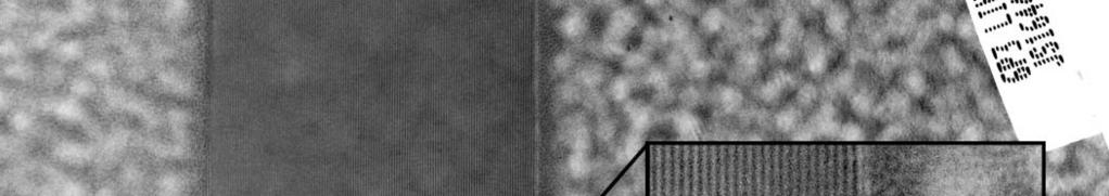
49 AFM image of silicon (111) atomic step specimen with native oxide See N.G. Orji et al. Wear 257, 1264 (2004).

")
")


50 Relation between miscut angle and average width of terraces Si(111) with 0.09 miscut Si(111) with miscut Samples after heating in UHV reveal single atomic terraces, and the average width of the terraces is nm/tanθ, θ θ the miscut angle.
51 Calibrated Atomic Force Microscope with AFM Sensor on Kinematic Mount
52 Comparison of Silicon Step Height Results
53 Ill t ti f St H i ht C l l ti Illustration of Step Height Calculation for a Single Profile


54 Typical Area Selection for Step Height Analysis on Si (111) What is the expected variability for a user? scan size is 1.44 µm
55 Results of Industrial Measurement Comparison Five participants, including NIST (using Nanoscope 3, not C-AFM) Table I. Summary of Fina l Results for Silic on Step Height Samples Participant Number of Topographic Images Average Step Height Value (pm) One Standard Average Numb er Number of Deviation of Steps in Areas (pm) Each Image Measured A B C D E Reference: R. Dixson et al. SPIE Proc. 4344, 157 (2001)
56 Developed by ASTM SC E42.14, STM/AFM
57 Observations The structure of NNI provides for strong coordination among agencies with different missions Nanoscale length metrology plays an important role in the semiconductor industry and in particle based nanotechnology and will be important in the manufacture of many other nano-scale components and functional features Probe-based based Microscopy is capable of nm uncertainties for width and pm-scale uncertainties for height of features on surfaces.


58 Probable Future Developments Probe-based microscopy to improve its capability for high- resolution probing of soft structures SEM image of Buckypaper, Chastek/Talbott NIST A. Vladar, He ion microscopy of 60 nm gold He ion microscope under development for nanoscale length measurement
Crystalline Surfaces for Laser Metrology
 Crystalline Surfaces for Laser Metrology A.V. Latyshev, Institute of Semiconductor Physics SB RAS, Novosibirsk, Russia Abstract: The number of methodological recommendations has been pronounced to describe
Chapter 10. Nanometrology. Oxford University Press All rights reserved.
 Chapter 10 Nanometrology Oxford University Press 2013. All rights reserved. 1 Introduction Nanometrology is the science of measurement at the nanoscale level. Figure illustrates where nanoscale stands
Nanocrystalline Cellulose:
 Nanocrystalline Cellulose: International Standardization & Metrological Approaches Alan Steele National Research Council Institute for National Measurement Standards TAPPI International Conference on Nano
Chapter 12. Nanometrology. Oxford University Press All rights reserved.
 Chapter 12 Nanometrology Introduction Nanometrology is the science of measurement at the nanoscale level. Figure illustrates where nanoscale stands in relation to a meter and sub divisions of meter. Nanometrology
Nanometrology and its role in the development of nanotechnology
 Nanometrology and its role in the development of nanotechnology Rob Bergmans Nederlands Meetinstituut Van Swinden Laboratorium 1 NMi Van Swinden Laboratorium The Art of Measurement Dutch national metrology
Nanomechanics Measurements and Standards at NIST
 Nanomechanics Measurements and Standards at NIST Robert F. Cook Deputy Chief, Ceramics Division Leader, Nanomechanical Properties Group robert.cook@nist.gov NIST Mission Promote U.S. innovation and industrial
Imaging Methods: Scanning Force Microscopy (SFM / AFM)
") Imaging Methods: Scanning Force Microscopy (SFM / AFM) The atomic force microscope (AFM) probes the surface of a sample with a sharp tip, a couple of microns long and often less than 100 Å in diameter.
Imaging Methods: Scanning Force Microscopy (SFM / AFM) The atomic force microscope (AFM) probes the surface of a sample with a sharp tip, a couple of microns long and often less than 100 Å in diameter.
Cross Section and Line Edge Roughness Metrology for EUV Lithography using Critical Dimension Small Angle X-ray X
 Cross Section and Line Edge Roughness Metrology for EUV Lithography using Critical Dimension Small Angle X-ray X Scattering Ronald L. Jones, Wen-li Wu, Eric K. Lin NIST Polymers Division, Gaithersburg,
MEMS Metrology. Prof. Tianhong Cui ME 8254
 MEMS Metrology Prof. Tianhong Cui ME 8254 What is metrology? Metrology It is the science of weights and measures Refers primarily to the measurements of length, weight, time, etc. Mensuration- A branch
T.V. Vorburger, J.F. Song, T.B. Renegar, and A. Zheng January 23, 2008
 NIST SURFACE ROUGHNESS AND STEP HEIGHT CALIBRATIONS: Measurement Conditions and Sources of Uncertainty T.V. Vorburger, J.F. Song, T.B. Renegar, and A. Zheng January 23, 2008 The property of surface roughness
Fabrication and Domain Imaging of Iron Magnetic Nanowire Arrays
 Abstract #: 983 Program # MI+NS+TuA9 Fabrication and Domain Imaging of Iron Magnetic Nanowire Arrays D. A. Tulchinsky, M. H. Kelley, J. J. McClelland, R. Gupta, R. J. Celotta National Institute of Standards
Reference nanometrology based on AFM, SEM and TEM techniques
 Reference nanometrology based on AFM, SEM and TEM techniques Abstract Gaoliang Dai, Wolfgang Häßler-Grohne, Jens Fluegge, Harald Bosse Physikalisch-Technische Bundesanstalt, 38116 Braunschweig, Germany
Sensors and Metrology. Outline
 Sensors and Metrology A Survey 1 Outline General Issues & the SIA Roadmap Post-Process Sensing (SEM/AFM, placement) In-Process (or potential in-process) Sensors temperature (pyrometry, thermocouples, acoustic
In the name of Allah
 In the name of Allah Nano chemistry- 4 th stage Lecture No. 1 History of nanotechnology 16-10-2016 Assistance prof. Dr. Luma Majeed Ahmed lumamajeed2013@gmail.com, luma.ahmed@uokerbala.edu.iq Nano chemistry-4
Standards for Physico-Chemical Measurements of Nanomaterials
 Standards for Physico-Chemical Measurements of Nanomaterials Debra L. Kaiser Technical Program Director Material Measurement Laboratory, NIST, US February 15, 2017 Outline of Presentation Introduction
Kavli Workshop for Journalists. June 13th, CNF Cleanroom Activities
 Kavli Workshop for Journalists June 13th, 2007 CNF Cleanroom Activities Seeing nm-sized Objects with an SEM Lab experience: Scanning Electron Microscopy Equipment: Zeiss Supra 55VP Scanning electron microscopes
Standards for Nanotechnology Workforce Education
 Standards for Nanotechnology Workforce Education Standards Development Organizations (SDOs) Global International Organization for Standardization International Electrotechnical Commission Regional European
METROLOGY AND STANDARDIZATION FOR NANOTECHNOLOGIES
 MEROLOGY AND SANDARDIZAION FOR NANOECHNOLOGIES P.A.odua Center for Surface and Vacuum Research (CSVR), Moscow, Moscow Institute of Physics and echnology (MIP) E-mail: fgupnicpv@mail.ru Key words: nanotechnology,
Like space travel and the Internet before it, the possibilities of the nano world catches the imagination of school children and scientists alike.
 The Nano World Preface Nano is the cool thing and it s the buzzword Like space travel and the Internet before it, the possibilities of the nano world catches the imagination of school children and scientists
High Precision Dimensional Metrology of Periodic Nanostructures using Laser Scatterometry
 High Precision Dimensional Metrology of Periodic Nanostructures using Laser Scatterometry B. Bodermann, S. Bonifer, E. Buhr, A. Diener, M. Wurm, Physikalisch-Technische Bundesanstalt, Braunschweig, Germany
Strong Coupling between On Chip Notched Ring Resonator and Nanoparticle
 Strong Coupling between On Chip Notched Ring Resonator and Nanoparticle S. Wang 1, K. Broderick 1, 3, H. Smith 1 2, 3,1 *, and Y. Yi 1 Massauchusetts Institute of Technology, Cambridge, MA 02139 2 New
MSN551 LITHOGRAPHY II
 MSN551 Introduction to Micro and Nano Fabrication LITHOGRAPHY II E-Beam, Focused Ion Beam and Soft Lithography Why need electron beam lithography? Smaller features are required By electronics industry:
Nanotechnology Nanofabrication of Functional Materials. Marin Alexe Max Planck Institute of Microstructure Physics, Halle - Germany
 Nanotechnology Nanofabrication of Functional Materials Marin Alexe Max Planck Institute of Microstructure Physics, Halle - Germany Contents Part I History and background to nanotechnology Nanoworld Nanoelectronics
Nanotechnology Fabrication Methods.
 Nanotechnology Fabrication Methods. 10 / 05 / 2016 1 Summary: 1.Introduction to Nanotechnology:...3 2.Nanotechnology Fabrication Methods:...5 2.1.Top-down Methods:...7 2.2.Bottom-up Methods:...16 3.Conclusions:...19
Remote Access to Hi-tech Equipment
 Remote Access to Hi-tech Equipment From Your Classroom to Ours Sebastien Maeder Outline What is Remote Access? The Method vs. the Goal The role within NACK Why should we try? Confines of Classroom Characterization
Mechanical Characterization of High Aspect Ratio Silicon Nanolines
 Mater. Res. Soc. Symp. Proc. Vol. 1086 2008 Materials Research Society 1086-U05-07 Mechanical Characterization of High Aspect Ratio Silicon Nanolines Bin Li 1, Huai Huang 1, Qiu Zhao 1, Zhiquan Luo 1,
Opportunities and Implications for. the 21st Century
 Opportunities and Implications for Green Nanotechnology in Industry for the 21st Century Reducing Principles to Practice June 16, 2010 John M. Miller, Ph.D. Dune Sciences, Inc. Nanotechnology CLEAN WATER
There's Plenty of Room at the Bottom
 There's Plenty of Room at the Bottom 12/29/1959 Feynman asked why not put the entire Encyclopedia Britannica (24 volumes) on a pin head (requires atomic scale recording). He proposed to use electron microscope
Nanoholes for leak metrology
 Vacuum Metrology for Industry Nanoholes for leak metrology Università Degli Studi di Genova, Italy OUTLINE INTRODUCTION FABRICATION OF NANOHOLES GEOMETRICAL CHARACTERIZATION LEAK DEVICES RESULTS: PTB INRIM
2D Materials Research Activities at the NEST lab in Pisa, Italy. Stefan Heun NEST, Istituto Nanoscienze-CNR and Scuola Normale Superiore, Pisa, Italy
 2D Materials Research Activities at the NEST lab in Pisa, Italy Stefan Heun NEST, Istituto Nanoscienze-CNR and Scuola Normale Superiore, Pisa, Italy 2D Materials Research Activities at the NEST lab in
Metrology for single nanometer manufacturing. Richard Koops, Arthur van de Nes, Marijn van Veghel
 Metrology for single nanometer manufacturing Richard Koops, Arthur van de Nes, Marijn van Veghel International MicroNano Conference Amsterdam, 13 December 2016 About VSL - National Metrology Institute
SPECIFIC USES OR APPLICATIONS OF NANOSTRUCTURES; MEASUREMENT OR ANALYSIS OF NANOSTRUCTURES; MANUFACTURE OR TREATMENT OF NANOSTRUCTURES
 CPC - B82Y - 2017.08 B82Y SPECIFIC USES OR APPLICATIONS OF NANOSTRUCTURES; MEASUREMENT OR ANALYSIS OF NANOSTRUCTURES; MANUFACTURE OR TREATMENT OF NANOSTRUCTURES Definition statement This place covers:
Graphene: Plane and Simple Electrical Metrology?
 Graphene: Plane and Simple Electrical Metrology? R. E. Elmquist, F. L. Hernandez-Marquez, M. Real, T. Shen, D. B. Newell, C. J. Jacob, and G. R. Jones, Jr. National Institute of Standards and Technology,
Removal of Cu Impurities on a Si Substrate by Using (H 2 O 2 +HF) and (UV/O 3 +HF)
 and (UV/O 3 +HF)") Journal of the Korean Physical Society, Vol. 33, No. 5, November 1998, pp. 579 583 Removal of Cu Impurities on a Si Substrate by Using (H 2 O 2 +HF) and (UV/O 3 +HF) Baikil Choi and Hyeongtag Jeon School
Journal of the Korean Physical Society, Vol. 33, No. 5, November 1998, pp. 579 583 Removal of Cu Impurities on a Si Substrate by Using (H 2 O 2 +HF) and (UV/O 3 +HF) Baikil Choi and Hyeongtag Jeon School
SEMATECH Knowledge Series 2010
 SEMATECH Knowledge Series 2010 Summary of the SEMATECH Workshop on Directed Self Assembly Lloyd Litt SEMATECH/GF Bill Hinsberg - IBM 20 October 2010 Kobe, Japan Copyright 2010 Advanced Materials Research
Nano Materials and Devices
 Nano Materials and Devices Professor Michael Austin Platform Technologies Research Institute Nano Materials and Devices Program Aim: to develop an integrated capability in nanotechnology Design and modelling
Nanomaterials and their Optical Applications
 Nanomaterials and their Optical Applications Winter Semester 2013 Lecture 02 rachel.grange@uni-jena.de http://www.iap.uni-jena.de/multiphoton Lecture 2: outline 2 Introduction to Nanophotonics Theoretical
Nanotechnology. Gavin Lawes Department of Physics and Astronomy
 Nanotechnology Gavin Lawes Department of Physics and Astronomy Earth-Moon distance 4x10 8 m (courtesy NASA) Length scales (Part I) Person 2m Magnetic nanoparticle 5x10⁻⁹ m 10 10 m 10 5 m 1 m 10-5 m 10-10
International Standardization for Measurement and Characterization of Nanomaterials
 2012/SOM2/SCSC/CON/008 International Standardization for Measurement and Characterization of Nanomaterials Submitted by: Japan 9 th Conference on Standards and Conformance in the Field of Innovations and
Lawrence Berkeley National Laboratory Lawrence Berkeley National Laboratory
 Lawrence Berkeley National Laboratory Lawrence Berkeley National Laboratory Title Spatial scaling metrics of mask-induced induced line-edge roughness Permalink https://escholarship.org/uc/item/5rc666c3
NANO SCIENCE AND TECHNOLOGY THE INDIAN SCENE
 NANO SCIENCE AND TECHNOLOGY THE INDIAN SCENE DR. PRAVEER ASTHANA MINISTRY OF SCIENCE AND TECHNOLOGY (DEPARTMENT OF SCIENCE AND TECHNOLOGY) GOVERNMENT OF INDIA WHAT HAVE WE DONE SO FAR? Basic Research in
Metrology is not a cost factor, but a profit center
 Edition February 2018 Semiconductor technology & processing Metrology is not a cost factor, but a profit center In recent years, remarkable progress has been made in the field of metrology, which is crucial
Fabrication at the nanoscale for nanophotonics
 Fabrication at the nanoscale for nanophotonics Ilya Sychugov, KTH Materials Physics, Kista silicon nanocrystal by electron beam induced deposition lithography Outline of basic nanofabrication methods Devices
Instrumentation and Operation
 Instrumentation and Operation 1 STM Instrumentation COMPONENTS sharp metal tip scanning system and control electronics feedback electronics (keeps tunneling current constant) image processing system data
Vapor-Phase Cutting of Carbon Nanotubes Using a Nanomanipulator Platform
 Vapor-Phase Cutting of Carbon Nanotubes Using a Nanomanipulator Platform MS&T 10, October 18, 2010 Vladimir Mancevski, President and CTO, Xidex Corporation Philip D. Rack, Professor, The University of
Quantum Information Science
 Quantum Information Science A Federal Perspective Dr. Altaf H. Carim at The Coming Quantum Revolution: Security and Policy Implications Hudson Institute Washington, DC October 17, 2017 Applications of
Opportunities for Advanced Plasma and Materials Research in National Security
 Opportunities for Advanced Plasma and Materials Research in National Security Prof. J.P. Allain allain@purdue.edu School of Nuclear Engineering Purdue University Outline: Plasma and Materials Research
ASTM International Committee E56 on Nanotechnology
 ASTM International Committee E56 on Nanotechnology http://www.astm.org/commit/committee/e56.htm Debra L. Kaiser Material Measurement Laboratory, NIST Vice-Chair, Committee E56 ANSI Panel Meeting February
Development of a nanostructural microwave probe based on GaAs
 Microsyst Technol (2008) 14:1021 1025 DOI 10.1007/s00542-007-0484-0 TECHNICAL PAPER Development of a nanostructural microwave probe based on GaAs Y. Ju Æ T. Kobayashi Æ H. Soyama Received: 18 June 2007
Nanolithography Techniques
 Nanolithography Techniques MSE 505 / MSNT 505 P. Coane Outline What Is Nanotechnology? The Motivation For Going Small Nanofabrication Technologies Basic Techniques Nano Lithography NANOTECHNOLOGY Nanotechnology
Direct-Write Deposition Utilizing a Focused Electron Beam
 Direct-Write Deposition Utilizing a Focused Electron Beam M. Fischer, J. Gottsbachner, S. Müller, W. Brezna, and H.D. Wanzenboeck Institute of Solid State Electronics, Vienna University of Technology,
CHARACTERIZING PROCESS SEMICONDUCTOR THIN FILMS WITH A CONFOCAL MICRO X-RAY FLUORESCENCE MICROSCOPE
 CHARACTERIZING PROCESS SEMICONDUCTOR THIN FILMS WITH A CONFOCAL MICRO X-RAY FLUORESCENCE MICROSCOPE 218 Chris M. Sparks 1, Elizabeth P. Hastings 2, George J. Havrilla 2, and Michael Beckstead 2 1. ATDF,
Lecture 3: Heterostructures, Quasielectric Fields, and Quantum Structures
 Lecture 3: Heterostructures, Quasielectric Fields, and Quantum Structures MSE 6001, Semiconductor Materials Lectures Fall 2006 3 Semiconductor Heterostructures A semiconductor crystal made out of more
Südliche Stadtmauerstr. 15a Tel: D Erlangen Fax:
 Curriculum Vitae Lionel Santinacci 19.10.1974 Nationality: French Südliche Stadtmauerstr. 15a Tel: + 49 9131 852 7587 D-91054 Erlangen Fax: + 49 9131 852 7582 Germany e-mail: lionel@ww.uni-erlangen.de
Supporting Information
 Electronic Supplementary Material (ESI) for Nanoscale. This journal is The Royal Society of Chemistry 2017 Supporting Information Poly(ferrocenylsilane) Electrolytes as Gold Nanoparticle Foundry: Two-in-
Nanostructure Fabrication Using Selective Growth on Nanosize Patterns Drawn by a Scanning Probe Microscope
 Nanostructure Fabrication Using Selective Growth on Nanosize Patterns Drawn by a Scanning Probe Microscope Kentaro Sasaki, Keiji Ueno and Atsushi Koma Department of Chemistry, The University of Tokyo,
master thesis STM studies of molecules for molecular electronics
 STM studies of molecules for molecular electronics Experimental study of single organic molecules by Scanning Tunneling Microscope (STM) and spectroscopy at low temperature Experimental STM images of Aza-BODIPY
Nanofabrication/Nano-Characterization Calixarene and CNT Control Technology
 Nanofabrication/Nano-Characterization Calixarene and CNT Control Technology ISHIDA Masahiko, FUJITA Junichi, NARIHIRO Mitsuru, ICHIHASHI Toshinari, NIHEY Fumiyuki, OCHIAI Yukinori Abstract The world of
Diamond-like-carbon (DLC) master creation for use in soft lithography using the Atomic Force Microscope (AFM)
 master creation for use in soft lithography using the Atomic Force Microscope (AFM)") Diamond-like-carbon (DLC) master creation for use in soft lithography using the Atomic Force Microscope (AFM) Author Watson, Gregory, Myhra, S., Watson, Jolanta Published 2007 Journal Title Journal of
Diamond-like-carbon (DLC) master creation for use in soft lithography using the Atomic Force Microscope (AFM) Author Watson, Gregory, Myhra, S., Watson, Jolanta Published 2007 Journal Title Journal of
General concept and defining characteristics of AFM. Dina Kudasheva Advisor: Prof. Mary K. Cowman
 General concept and defining characteristics of AFM Dina Kudasheva Advisor: Prof. Mary K. Cowman Overview Introduction History of the SPM invention Technical Capabilities Principles of operation Examples
SIB61 CRYSTAL. Report Status: PU
 Final Publishable JRP Summary for SIB61 CRYSTAL Crystalline surfaces, self-assembled structures, and nano-origami as length standards in (nano)metrology Overview Nanotechnology covers materials with dimensions
National Nanotechnology Initiative Overview and Perspective: Department of Defense
 National Nanotechnology Initiative Overview and Perspective: Department of Defense Dr. David M. Stepp david.m.stepp@us.army.mil (919) 549-4329, DSN 832-4329, FAX (919) 549-4399 23 March 2005 Outline Department
Scanning Tunneling Microscopy
 Scanning Tunneling Microscopy Scanning Direction References: Classical Tunneling Quantum Mechanics Tunneling current Tunneling current I t I t (V/d)exp(-Aφ 1/2 d) A = 1.025 (ev) -1/2 Å -1 I t = 10 pa~10na
Sensors and Metrology
 Sensors and Metrology A Survey 1 Outline General Issues & the SIA Roadmap Post-Process Sensing (SEM/AFM, placement) In-Process (or potential in-process) Sensors temperature (pyrometry, thermocouples, acoustic
There s plenty of room at the bottom! - R.P. Feynman, Nanostructure: a piece of material with at least one dimension less than 100 nm in extent.
 Nanostructures and Nanotechnology There s plenty of room at the bottom! - R.P. Feynman, 1959 Materials behave differently when structured at the nm scale than they do in bulk. Technologies now exist that
State of São Paulo. Brasil. Localization. Santo André
 Brasil State of São Paulo Localization Santo André The Group www.crespilho.com Frank N. Crespilho Pablo R. S. Abdias Group Leader Synthesis of nanostructured materials using polyelectrolytes Andressa R.
In today s lecture, we will cover:
 In today s lecture, we will cover: Metal and Metal oxide Nanoparticles Semiconductor Nanocrystals Carbon Nanotubes 1 Week 2: Nanoparticles Goals for this section Develop an understanding of the physical
Optical Design for Affordable EUV Lithography Michael Goldstein, Ph.D. Vivek Bakshi, Ph.D. October 31, 2007
 Optical Design for Affordable EUV Lithography Michael Goldstein, Ph.D. Vivek Bakshi, Ph.D. October 31, 2007 Advanced Materials Research Center, AMRC, International SEMATECH Manufacturing Initiative, and
Gold nanothorns macroporous silicon hybrid structure: a simple and ultrasensitive platform for SERS
 Supporting Information Gold nanothorns macroporous silicon hybrid structure: a simple and ultrasensitive platform for SERS Kamran Khajehpour,* a Tim Williams, b,c Laure Bourgeois b,d and Sam Adeloju a
The Cylindrical Envelope Projection Model Applied to SE Images of Curved Surfaces and Comparison with AFM Evaluations
 07.80 The Microsc. Microanal. Microstruct. 513 Classification Physics Abstracts - - 06.20 61.16P The Cylindrical Envelope Projection Model Applied to SE Images of Curved Surfaces and Comparison with AFM
Basic Laboratory. Materials Science and Engineering. Atomic Force Microscopy (AFM)
") Basic Laboratory Materials Science and Engineering Atomic Force Microscopy (AFM) M108 Stand: 20.10.2015 Aim: Presentation of an application of the AFM for studying surface morphology. Inhalt 1.Introduction...
Basic Laboratory Materials Science and Engineering Atomic Force Microscopy (AFM) M108 Stand: 20.10.2015 Aim: Presentation of an application of the AFM for studying surface morphology. Inhalt 1.Introduction...
High-resolution Characterization of Organic Ultrathin Films Using Atomic Force Microscopy
 High-resolution Characterization of Organic Ultrathin Films Using Atomic Force Microscopy Jing-jiang Yu Nanotechnology Measurements Division Agilent Technologies, Inc. Atomic Force Microscopy High-Resolution
NANOTECHNOLOGY SOLID WASTE IMPLICATIONS. Gurumurthy Ramachandran. University of Minnesota
 NANOTECHNOLOGY SOLID WASTE IMPLICATIONS Gurumurthy Ramachandran University of Minnesota Engineering at the Atomic Level: Scanning Tunneling Microscopy Manipulating atoms Writing with atoms. D.M. Eigler,
Nanostructure. Materials Growth Characterization Fabrication. More see Waser, chapter 2
 Nanostructure Materials Growth Characterization Fabrication More see Waser, chapter 2 Materials growth - deposition deposition gas solid Physical Vapor Deposition Chemical Vapor Deposition Physical Vapor
Nanoelectronics 09. Atsufumi Hirohata Department of Electronics. Quick Review over the Last Lecture
 Nanoelectronics 09 Atsufumi Hirohata Department of Electronics 13:00 Monday, 12/February/2018 (P/T 006) Quick Review over the Last Lecture ( Field effect transistor (FET) ): ( Drain ) current increases
Materials. Definitions of nanotechnology. The term nanotechnology was invented by Professor Norio Taniguchi at the University of Tokyo in 1971.
 Materials Definitions of nanotechnology The term nanotechnology was invented by Professor Norio Taniguchi at the University of Tokyo in 1971. The original definition, translated into English Nano-technology'
Technologies VII. Alternative Lithographic PROCEEDINGS OF SPIE. Douglas J. Resnick Christopher Bencher. Sponsored by. Cosponsored by.
 PROCEEDINGS OF SPIE Alternative Lithographic Technologies VII Douglas J. Resnick Christopher Bencher Editors 23-26 February 2015 San Jose, California, United States Sponsored by SPIE Cosponsored by DNS
nano-ta: Nano Thermal Analysis
 nano-ta: Nano Thermal Analysis Application Note #1 Failure Analysis - Identification of Particles in a Polymer Film Author: David Grandy Ph.D. Introduction Nano-TA is a local thermal analysis technique
EUREKA: A new Industry EUV Research Center at LBNL
 EUREKA: A new Industry EUV Research Center at LBNL Patrick Naulleau Center for X-ray Optics Lawrence Berkeley National Laboratory Berkeley Lab MSD Materials Sciences Division 1 Operating model Core operational
MICRO-SCALE SHEET RESISTANCE MEASUREMENTS ON ULTRA SHALLOW JUNCTIONS
 MICRO-SCALE SHEET RESISTANCE MEASUREMENTS ON ULTRA SHALLOW JUNCTIONS Christian L. Petersen, Rong Lin, Dirch H. Petersen, Peter F. Nielsen CAPRES A/S, Burnaby, BC, Canada CAPRES A/S, Lyngby, Denmark We
Green nanoscience: Opportunities and challenges for innovation
 Green nanoscience: Opportunities and challenges for innovation Jim Hutchison Department of Chemistry, University of Oregon Director, UO Materials Science Institute Director, ONAMI Safer Nanomaterials and
Electron-beam SAFIER process and its application for magnetic thin-film heads
 Electron-beam SAFIER process and its application for magnetic thin-film heads XiaoMin Yang, a) Harold Gentile, Andrew Eckert, and Stanko R. Brankovic Seagate Research Center, 1251 Waterfront Place, Pittsburgh,
MICRO-FOUR-POINT PROBES IN A UHV SCANNING ELECTRON MICROSCOPE FOR IN-SITU SURFACE-CONDUCTIVITY MEASUREMENTS
 Surface Review and Letters, Vol. 7, Nos. 5 & 6 (2000) 533 537 c World Scientific Publishing Company MICRO-FOUR-POINT PROBES IN A UHV SCANNING ELECTRON MICROSCOPE FOR IN-SITU SURFACE-CONDUCTIVITY MEASUREMENTS
Nanoparticle Devices. S. A. Campbell, ECE C. B. Carter, CEMS H. Jacobs, ECE J. Kakalios, Phys. U. Kortshagen, ME. Institute of Technology
 Nanoparticle Devices S. A. Campbell, ECE C. B. Carter, CEMS H. Jacobs, ECE J. Kakalios, Phys. U. Kortshagen, ME Applications of nanoparticles Flash Memory Tiwari et al., Appl. Phys. Lett. 68, 1377, 1996.
Contents. Preface...xv List of Contributors...xvii
 Preface...xv List of Contributors...xvii CHAPTER 1 Nanotechnology to Nanomanufacturing... 1 1.1 Introduction...1 1.2 Approaches to Nanotechnology...2 1.3 Transition from Nanotechnology to Nanomanufacturing...3
ESH Benign Processes for he Integration of Quantum Dots (QDs)
") ESH Benign Processes for he Integration of Quantum Dots (QDs) PIs: Karen K. Gleason, Department of Chemical Engineering, MIT Graduate Students: Chia-Hua Lee: PhD Candidate, Department of Material Science
ESH Benign Processes for he Integration of Quantum Dots (QDs) PIs: Karen K. Gleason, Department of Chemical Engineering, MIT Graduate Students: Chia-Hua Lee: PhD Candidate, Department of Material Science
Carbon Nanotube Reference Materials and Characterization Jeffrey A. Fagan
 Carbon Nanotube Reference Materials and Characterization Jeffrey A. Fagan National Institute of Standards and Technology Gaithersburg, MD Nanotube Market Composites Energy Electronics Chemical & Engineering
Photoacoustic metrology of nanoimprint polymers
 Photoacoustic metrology of nanoimprint polymers T. Kehoe a, J. Bryner b, J. Vollmann b, C. Sotomayor Torres a, L. Aebi b and J. Dual b a Tyndall National Institute, Lee Maltings, University College Cork,
Positioning, Structuring and Controlling with Nanoprecision
 Positioning, Structuring and Controlling with Nanoprecision Regine Hedderich 1,2, Tobias Heiler 2,3, Roland Gröger 2,3, Thomas Schimmel 2,3 and Stefan Walheim 2,3 1 Network NanoMat 2 Institute of Nanotechnology,
From nanophysics research labs to cell phones. Dr. András Halbritter Department of Physics associate professor
 From nanophysics research labs to cell phones Dr. András Halbritter Department of Physics associate professor Curriculum Vitae Birth: 1976. High-school graduation: 1994. Master degree: 1999. PhD: 2003.
Nanoscale IR spectroscopy of organic contaminants
 The nanoscale spectroscopy company The world leader in nanoscale IR spectroscopy Nanoscale IR spectroscopy of organic contaminants Application note nanoir uniquely and unambiguously identifies organic
Contents. What is AFM? History Basic principles and devices Operating modes Application areas Advantages and disadvantages
 Contents What is AFM? History Basic principles and devices Operating modes Application areas Advantages and disadvantages Figure1: 2004 Seth Copen Goldstein What is AFM? A type of Scanning Probe Microscopy
Measurement of hardness, surface potential, and charge distribution with dynamic contact mode electrostatic force microscope
 REVIEW OF SCIENTIFIC INSTRUMENTS VOLUME 70, NUMBER 3 MARCH 1999 Measurement of hardness, surface potential, and charge distribution with dynamic contact mode electrostatic force microscope J. W. Hong,
29: Nanotechnology. What is Nanotechnology? Properties Control and Understanding. Nanomaterials
 29: Nanotechnology What is Nanotechnology? Properties Control and Understanding Nanomaterials Making nanomaterials Seeing at the nanoscale Quantum Dots Carbon Nanotubes Biology at the Nanoscale Some Applications
custom reticle solutions
 custom reticle solutions 01 special micro structures Pyser Optics has over 60 years experience in producing high quality micro structure products. These products are supplied worldwide to industries including
Nanostrukturphysik (Nanostructure Physics)
") Nanostrukturphysik (Nanostructure Physics) Prof. Yong Lei & Dr. Yang Xu Fachgebiet 3D-Nanostrukturierung, Institut für Physik Contact: yong.lei@tu-ilmenau.de; yang.xu@tu-ilmenau.de Office: Unterpoerlitzer
Nanostrukturphysik (Nanostructure Physics) Prof. Yong Lei & Dr. Yang Xu Fachgebiet 3D-Nanostrukturierung, Institut für Physik Contact: yong.lei@tu-ilmenau.de; yang.xu@tu-ilmenau.de Office: Unterpoerlitzer
ETH Rüschlikon the people and their research
 ETH Zurich @ Rüschlikon the people and their research Prof. Dr. Dimos Poulikakos, Laboratory of Thermodynamics in Emerging Technologies and Coordinator of the Nanotechnology Center, ETH Zurich The Vision
Techniken der Oberflächenphysik (Technique of Surface Physics)
") Techniken der Oberflächenphysik (Technique of Surface Physics) Yong Lei & Fabian Grote Fachgebiet 3D-Nanostrukturierung, Institut für Physik Contact: yong.lei@tu-ilmenau.de; fabian.grote@tu-ilmenau.de
Techniken der Oberflächenphysik (Technique of Surface Physics) Yong Lei & Fabian Grote Fachgebiet 3D-Nanostrukturierung, Institut für Physik Contact: yong.lei@tu-ilmenau.de; fabian.grote@tu-ilmenau.de
Scattering-type near-field microscopy for nanoscale optical imaging
 Scattering-type near-field microscopy for nanoscale optical imaging Rainer Hillenbrand Nano-Photonics Group Max-Planck-Institut für Biochemie 82152 Martinsried, Germany Infrared light enables label-free
Final Reading Assignment: Travels to the Nanoworld: pages pages pages
 Final Reading Assignment: Travels to the Nanoworld: pages 152-164 pages 201-214 pages 219-227 Bottom-up nanofabrication Can we assemble nanomachines manually? What are the components (parts)? nanoparticles