Nanofluidics and 2D Materials Based Nanosensors. Ivan Vlassiouk Oak Ridge National Laboratory, TN, USA
|
|
|
- Cory Simon
- 5 years ago
- Views:
Transcription


1 Nanofluidics and 2D Materials Based Nanosensors Ivan Vlassiouk Oak Ridge National Laboratory, TN, USA
2 Outline What are nanosensors and why do we need them? Learning from Nature is the key! Microfluidics vs Nanofludics Examples of Nanosensors based on nanofluidics Fluidic electronics Graphene based membranes for sensing Future outlook


3 Oak Ridge National Laboratory 40 km staff ORNL major expertise: - Engineering - Material Science - Supercomputing ~18 petaflops Memory: 710 TB Storage: 10 PB Power: 8 MW


4 Sensors vs Nanosensors Sensors are used virtually in every device: from smartphones to cars and biotechnology We can sense different phenomena and objects of various scales From Earthquakes, Supernovas and Relic Radiation to Higgs Boson. LHC: Images.google.com


5 Sensors vs Nanosensors Atoms Molecules Electronics Viruses Nanosensors allow for INTEGRATION of many sensing elements in small volume nanometers microns Connection between nano and macro world: - Neural interface: connection between living species and electronics - Artificial cells. - Bionics

6 Lessons from Nature: Perfect Sensors Arrangement Wall of a cell is an impermeable lipid (fat) membrane i.e. BARRIER Pores in the membrane are smart holes Sensitive to - Light - Voltage - Chemicals - Temperature


. R. MacKinnon, P.")
. S. Berneche, B.")
7 Examples of Biological Channels A potassium selective channel is a very important player in the nerve signaling. < 1 nm Potassium selective channel with four K + in the selectivity filter (right panel). R. MacKinnon, P. Agre 2003 E. Gouaux, R. MacKinnon, Science 310, 1461 (2005). S. Berneche, B.Roux, Nature 414, 73 (2001).


8 What the Nanofluidics is? In a macro channel ions can not interact with the channel wall significantly images.google.com m If the size of the channel is small, ions can interact with the surface!! - Size of the channel - Surface energy - Surface Charge - Chemical modification - Electrostatic forces <100 nm


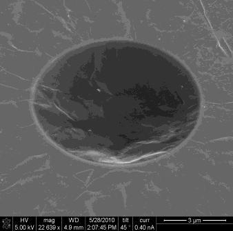
9 Volume exclusion DNA sensor and purification D c D p Metal D b Vlassiouk et al. Langmuir, 20, 9913; Vlassiouk et al, 21, 4776


10 Light sensitive channels Nature example - Channelrhodopsin We employ hydrophobic interactions! Z, 10 6 A 337 nm on 532 nm on Resistance drops after UV irradiation B C D E 0 1x10 3 2x10 3 3x10 3 4x10 3 5x10 3 6x10 3 Time, s Vlassiouk et al, Nanolett, 2006,


11 Old technique for new applications: preparation of ion channel 1. Irradiation with e.g. Xe, Au, U Darmstadt, Germany E. Loriot Dubna, Russia 2. Chemical etching 1 ion 1 latent track 1 pore! R.L. Fleischer, P.B. Price, R.M. Walker (1975)
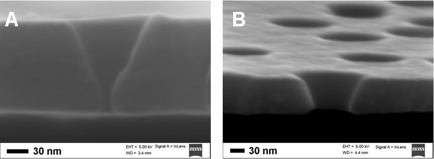
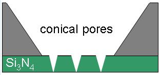
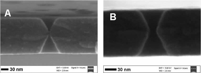
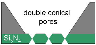
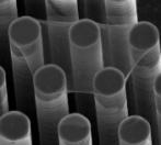
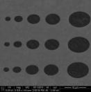
12 Fabrication of nanopores array in SiN Vlassiouk et al, PNAS, 2009, 106, 21039


13 Electrostatics paramount for nanofluidics based nanosensors. Microchannels concentrations of positive and negative ions are equal. Nanochannels small volume but large surface: concentration of counter ions is higher! C 2 er
14 How to Make an Ionic diode? _ I. Vlassiouk, Z.S. Siwy, Nano Lett. 7, 553 (2007) Depletion zone H. Daiguji, P. Yang, A. Majumdar, NanoLett., 4, 137 (2005).
15 OPEN State of Ionic Diode _ BIPOLAR DEVICE current carried by both
 I( 5V ) -5-4 -3-2 -1 0 1 2 3 4 5 Voltage (V) 200 5 nm")
 61 I( 5V ) I. Vlassiouk, Z.S. Siwy, Nano Lett.")
16 Ionic Bipolar Diodes Current (na) Current (na) I( 5V ) I( 5V ) Voltage (V) nm pore Voltage (V) I( 5V ) 61 I( 5V ) I. Vlassiouk, Z.S. Siwy, Nano Lett. 7, 553 (2007);

17 1D Analytical solution l n, p N N a d V N N 2e d 1 a 0 doping I Current open ev 1 gen gen k T B Ih Ie e Depletion zone Va l dep 0 I BP open _ _ ea 2k BT Current 2 a pore radius - surface charge density edc L V V 2 o Voltage Voltage I closed I gen h gen e N.W. Ashcroft, N.D. Mermin, Solid State Physics, Thomas Learning, 1976 I I BP closed 2e 3 2 a C D L 2 bulk I. Vlassiouk, S. Smirnov, Z. Siwy, ACS Nano 2, 1589 (2008)
 8 6 4 2")
 -4-6 Tip modified")
18 Biosensing with Nanofluidic Diodes. Biotin - Avidin {+;-} Avidin Biotin Current (na) Avidin is positive! biotin {-;-} Voltage (V) -4-6 Tip modified with biotin Avidin on top Vlassiouk et al, JACS, 2009, 131, 8211
19 Biosensing with Nanofluidic Diodes. Streptavidin. ph meter. Rectification degree I(-2V)/I(+2V) Current (na) {+;-} ph Voltage (V) -1.0 ph 5.8 {-;-} ph pi ph Vlassiouk et al, JACS, 2009, 131, 8211


20 Graphene atomically thin layer of carbon - Transparent - Flexible - High Electrical conductivity - High Thermal Conductivity - Exceptional Mechanical Strength Unique properties define wide range of applications: Applications Area 1 Transparent conductor: - Touch Screens - Solar Cells - Solid State Lighting - Smart Windows - LCD Displays Applications Area 2 Active component: - Electronics - Optoelectronics - RF devices - Communication - Sensing


21 Graphene: Perfect membrane? Perfect for - Desalination - Separation Graphene suspended structure fabrication: Aquaporin:


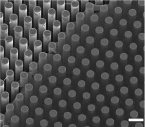
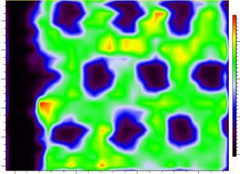
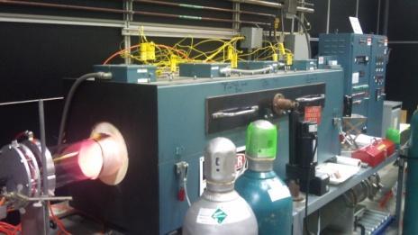
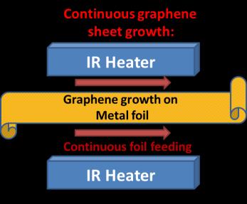
22 Good quality, Large Quantity 1 mm crystals 40 continues film A C B D x cm -1 Vlassiouk et al, Nanotechnology, 2011, 22, ; Vlassiouk et al, ACS Nano, 2011, 5, 6069; Vlassiouk et al, Carbon, 2013, 54, 58; Vlassiouk et al, J. Phys. Chem. C, 2013, 117, 18919


23 Future outlook - Personalized medicine - Bionics / mimicking the Nature - Neural interface google.images.com
Current Rectification of a Single Charged Conical nanopore. Qi Liu, Peking University Mentor: Prof. Qi Ouyang and Yugangwang
 Current Rectification of a Single Charged Conical nanopore Qi Liu, Peking University Mentor: Prof. Qi Ouyang and Yugangwang Biological Nanopores Biological ion channels are the principal nanodevices mediating
arxiv: v1 [cond-mat.soft] 10 Sep 2013
![arxiv: v1 [cond-mat.soft] 10 Sep 2013](/thumbs/82/86227302.jpg "arxiv: v1 [cond-mat.soft] 10 Sep 2013") Poisson-Nernst-Planck Model of Bipolar Nanofluidic Diode Based on Bulletlike Nanopore arxiv:139.39v1 [cond-mat.soft] 1 Sep 13 Abstract Li-Jian Qu a, Xinghua Zhang b, Jie Fu a, Lin Li c, Dadong Yan a, a
Poisson-Nernst-Planck Model of Bipolar Nanofluidic Diode Based on Bulletlike Nanopore arxiv:139.39v1 [cond-mat.soft] 1 Sep 13 Abstract Li-Jian Qu a, Xinghua Zhang b, Jie Fu a, Lin Li c, Dadong Yan a, a
There's Plenty of Room at the Bottom
 There's Plenty of Room at the Bottom 12/29/1959 Feynman asked why not put the entire Encyclopedia Britannica (24 volumes) on a pin head (requires atomic scale recording). He proposed to use electron microscope
Introduction to Molecular Electronics. Lecture 1: Basic concepts
 Introduction to Molecular Electronics Lecture 1: Basic concepts Conductive organic molecules Plastic can indeed, under certain circumstances, be made to behave very like a metal - a discovery for which
Micro/nano and precision manufacturing technologies and applications
 The 4th China-American Frontiers of Engineering Symposium Micro/nano and precision manufacturing technologies and applications Dazhi Wang School of Mechanical Engineering Dalian University of Technology
Nanomaterials and Their Environmental Applications Jason K. Holt (CTO, NanOasis) GA-FOE Presentation, 29 March 2012
 GA-FOE Presentation, 29 March 2012") Nanomaterials and Their Environmental Applications Jason K. Holt (CTO, NanOasis) GA-FOE Presentation, 29 March 2012 1 Nanomaterials - definitions Source: US EPA www.epa.gov 2 What are nanomaterials useful
Nanomaterials and Their Environmental Applications Jason K. Holt (CTO, NanOasis) GA-FOE Presentation, 29 March 2012 1 Nanomaterials - definitions Source: US EPA www.epa.gov 2 What are nanomaterials useful
Nanopores with controlled profiles in track-etched membranes
 NUKLEONIKA 2012;57(4):575 579 ORIGINAL PAPER Nanopores with controlled profiles in track-etched membranes Bożena A. Sartowska, Oleg L. Orelovitch, Adam Presz, Pavel Yu. Apel, Irina V. Blonskaya Abstract.
Electrolyte Concentration Dependence of Ion Transport through Nanochannels
 Electrolyte Concentration Dependence of Ion Transport through Nanochannels Murat Bakirci mbaki001@odu.edu Yunus Erkaya yerka001@odu.edu ABSTRACT The magnitude of current through a conical nanochannel filled
Simulation of ionic current through the nanopore in a double-layered semiconductor
 Home Search Collections Journals About Contact us My IOPscience Simulation of ionic current through the nanopore in a double-layered semiconductor membrane This article has been downloaded from IOPscience.
From nanophysics research labs to cell phones. Dr. András Halbritter Department of Physics associate professor
 From nanophysics research labs to cell phones Dr. András Halbritter Department of Physics associate professor Curriculum Vitae Birth: 1976. High-school graduation: 1994. Master degree: 1999. PhD: 2003.
Lecture 18: Microfluidic MEMS, Applications
 MECH 466 Microelectromechanical Systems University of Victoria Dept. of Mechanical Engineering Lecture 18: Microfluidic MEMS, Applications 1 Overview Microfluidic Electrokinetic Flow Basic Microfluidic
Nanotechnology? Source: National Science Foundation (NSF), USA
, USA") 2 2 Nanotechnology? Ability to work at the atomic, molecular and even sub-molecular levels in order to create and use material structures, devices and systems with new properties and functions Source:
2 2 Nanotechnology? Ability to work at the atomic, molecular and even sub-molecular levels in order to create and use material structures, devices and systems with new properties and functions Source:
Selective Molecular Transport through Intrinsic Defects in a Single Layer of CVD Graphene
 Selective Molecular Transport through Intrinsic Defects in a Single Layer of CVD Graphene Sean C. O Hern, Cameron A. Stewart, Michael S. H. Boutilier, Juan-Carlos Idrobo, Sreekar Bhaviripudi, Sarit K.
Field-effect reconfigurable nanofluidic ionic diodes
 Received 9 Apr Accepted Sep Published 8 Oct DOI:.8/ncomms5 Field-effect reconfigurable nanofluidic ionic diodes Weihua Guan, Rong Fan & Mark A. Reed, Several types of nanofluidic devices based on nanopores
Nanoscale electrochemistry
 Electrical characterisation of nanoscale samples & biochemical interfaces: methods and electronic instrumentation Nanoscale electrochemistry Giorgio Ferrari Dipartimento di elettronica, informazione e
Supporting Information for
 Supporting Information for Oscillatory Reaction Induced Periodic C-Quadruplex DNA Gating of Artificial Ion Channels Jian Wang, Ruochen Fang, Jue Hou, Huacheng Zhang, *, Ye Tian, *, Huanting Wang, and Lei
Lectures Graphene and
 Lectures 15-16 Graphene and carbon nanotubes Graphene is atomically thin crystal of carbon which is stronger than steel but flexible, is transparent for light, and conducts electricity (gapless semiconductor).
Computational Materials Design and Discovery Energy and Electronic Applications Synthesis Structure Properties
 Computational Materials Design and Discovery Energy and Electronic Applications Synthesis Structure Properties Supercapacitors Rechargeable batteries Supercomputer Photocatalysts Fuel cell catalysts First
UNIT I: Electronic Materials.
 SIDDHARTH INSTITUTE OF ENGINEERING & TECHNOLOGY :: PUTTUR Siddharth Nagar, Narayanavanam Road 517583 QUESTION BANK (DESCRIPTIVE) Subject with Code: SEMICONDUCTOR PHYSICS (18HS0851) Course & Branch: B.Tech
Multilayered Semiconductor Membranes for Nanopore Ionic Conductance Modulation
 Article Multilayered Semiconductor Membranes for Nanopore Ionic Conductance Modulation Maria E. Gracheva, Dmitriy V. Melnikov, and Jean-Pierre Leburton ACS Nano, 2008, 2 (11), 2349-2355 Publication Date
Low-adsorbing track-etched membrane
 Low-adsorbing track-etched membrane Pulane Mokoena, Mantwa Lephoto and Hlamulo Makelane Supervisor: Prof. Alexander Nechaeff Flerov Laboratory, JINR, DUBNA, September 2014 Outline Introduction Methodology
29: Nanotechnology. What is Nanotechnology? Properties Control and Understanding. Nanomaterials
 29: Nanotechnology What is Nanotechnology? Properties Control and Understanding Nanomaterials Making nanomaterials Seeing at the nanoscale Quantum Dots Carbon Nanotubes Biology at the Nanoscale Some Applications
Regulació electrostàtica de canals microfluídics i porus biològics. Jordi Faraudo Institut de Ciència de Materials de Barcelona
 Regulació electrostàtica de canals microfluídics i porus biològics Jordi Faraudo Institut de Ciència de Materials de Barcelona A few (interesting?) examples of nanofluidic devices Electrostatic regulation
Supporting Information
 Supporting Information Oh et al. 10.1073/pnas.0811923106 SI Text Hysteresis of BPE-PTCDI MW-TFTs. Fig. S9 represents bidirectional transfer plots at V DS 100VinN 2 atmosphere for transistors constructed
Nanostrukturphysik (Nanostructure Physics)
") Nanostrukturphysik (Nanostructure Physics) Prof. Yong Lei & Dr. Yang Xu Fachgebiet 3D-Nanostrukturierung, Institut für Physik Contact: yong.lei@tu-ilmenau.de; yang.xu@tu-ilmenau.de Office: Unterpoerlitzer
Nanostrukturphysik (Nanostructure Physics) Prof. Yong Lei & Dr. Yang Xu Fachgebiet 3D-Nanostrukturierung, Institut für Physik Contact: yong.lei@tu-ilmenau.de; yang.xu@tu-ilmenau.de Office: Unterpoerlitzer
Observation of ionic Coulomb blockade in nanopores
 Observation of ionic Coulomb blockade in nanopores Jiandong Feng 1 *, Ke Liu 1, Michael Graf 1, Dumitru Dumcenco 2, Andras Kis 2, Massimiliano Di Ventra 3, & Aleksandra Radenovic 1 * 1 Laboratory of Nanoscale
ION AND MOLECULE TRANSPORT IN NANOCHANNELS by. Li-Jing Cheng
 ION AND MOLECULE TRANSPORT IN NANOCHANNELS by Li-Jing Cheng A dissertation submitted in partial fulfillment of the requirements for the degree of Doctor of Philosophy Electrical Engineering and Computer
Lecture 2. Methods and Techniques for Self-assembly
 10.524 Lecture 2. Methods and Techniques for Self-assembly Instructor: Prof. Zhiyong Gu (Chemical Engineering & UML CHN/NCOE Nanomanufacturing Center) Lecture 2: Methods and Techniques for Self-assembly
ESS 5855 Surface Engineering for. MicroElectroMechanicalechanical Systems. Fall 2010
 ESS 5855 Surface Engineering for Microelectromechanical Systems Fall 2010 MicroElectroMechanicalechanical Systems Miniaturized systems with integrated electrical and mechanical components for actuation
Origin of the Electrophoretic Force on DNA in a Nanopore
 Origin of the Electrophoretic Force on DNA in a Nanopore Stijn van Dorp 1 Ulrich F. Keyser 2, *Nynke H. Dekker 1, Cees Dekker 1, Serge G. Lemay 1 1 Kavli Institut of Nanoscience, Delft University of Technology,
Ionic Transport in Microhole Fluidic Diodes Based on Asymmetric Ionomer Film Deposits
 DOI: 0.00/celc.000 0 0 0 0 0 Ionic Transport in Microhole Fluidic Diodes Based on Asymmetric Ionomer Film Deposits Klaus Mathwig,* [a] Barak D. B. Aaronson, [b] and Frank Marken* [b] Microhole fluidic
1. Depleted heterojunction solar cells. 2. Deposition of semiconductor layers with solution process. June 7, Yonghui Lee
 1. Depleted heterojunction solar cells 2. Deposition of semiconductor layers with solution process June 7, 2016 Yonghui Lee Outline 1. Solar cells - P-N junction solar cell - Schottky barrier solar cell
Solutions for Assignment-8
 Solutions for Assignment-8 Q1. The process of adding impurities to a pure semiconductor is called: [1] (a) Mixing (b) Doping (c) Diffusing (d) None of the above In semiconductor production, doping intentionally
MOS Capacitors ECE 2204
 MOS apacitors EE 2204 Some lasses of Field Effect Transistors Metal-Oxide-Semiconductor Field Effect Transistor MOSFET, which will be the type that we will study in this course. Metal-Semiconductor Field
Origin of the Electrophoretic Force on DNA in Nanopores. Biological and Soft Systems - Cavendish Laboratory
 Origin of the Electrophoretic Force on DNA in Nanopores Ulrich F. Keyser Biological and Soft Systems - Cavendish Laboratory Acknowledgements Delft Cees Dekker, Nynke H. Dekker, Serge G. Lemay R. Smeets,
Supplementary information for
 Supplementary information for Transverse electric field dragging of DNA in a nanochannel Makusu Tsutsui, Yuhui He, Masayuki Furuhashi, Rahong Sakon, Masateru Taniguchi & Tomoji Kawai The Supplementary
Fadei Komarov Alexander Kamyshan
 Fadei Komarov Alexander Kamyshan Institute of Applied Physics Problems, Belarusian State University, Minsk, Belarus KomarovF@bsu.by Tasks and Objects 2 Introduction and motivation Experimental setup designed
In this study, we have investigated a new method to determine the pi values of proteins compared to the
 K. Keçeci / Hacettepe J. Biol. & Chem., 2016, 44 (4), 401 407 Isoelectric Point Determination of Proteins Using Track- Etched Single-Nanopore Membrane İz-Aşındırılmış Tekli Nano Membran Kullanarak Proteinlerin
Wafer-scale fabrication of graphene
 Wafer-scale fabrication of graphene Sten Vollebregt, MSc Delft University of Technology, Delft Institute of Mircosystems and Nanotechnology Delft University of Technology Challenge the future Delft University
Computational Modeling of Molecular Electronics. Chao-Cheng Kaun
 Computational Modeling of Molecular Electronics Chao-Cheng Kaun Research Center for Applied Sciences, Academia Sinica Department of Physics, National Tsing Hua University May 9, 2007 Outline: 1. Introduction
Carbon Nanotube Thin-Films & Nanoparticle Assembly
 Nanodevices using Nanomaterials : Carbon Nanotube Thin-Films & Nanoparticle Assembly Seung-Beck Lee Division of Electronics and Computer Engineering & Department of Nanotechnology, Hanyang University,
Session V: Graphene. Matteo Bruna CAMBRIDGE UNIVERSITY DEPARTMENT OF ENGINEERING
 Session V: Graphene Matteo Bruna Graphene: Material in the Flatland Graphite Graphene Properties: Thinnest imaginable material Good(and tunable) electrical conductor Strongest ever measured Stiffest known
Chemie en Technologie van Materialen (Materials Science and Technology)
") ST module 8b Chemie en Technologie van Materialen (Materials Science and Technology) 2018-19 201600135 Module coordinator: dr.ir. Evert Houwman Chemie en Technologie van Materialen Materials Science and
ST module 8b Chemie en Technologie van Materialen (Materials Science and Technology) 2018-19 201600135 Module coordinator: dr.ir. Evert Houwman Chemie en Technologie van Materialen Materials Science and
Engineered Flexible Conductive Barrier Films for Advanced Energy Devices
 The 13 th Korea-U.S. Forum on Nanotechnology Engineered Flexible Conductive Barrier Films for Advanced Energy Devices Jinsung Kwak 1, Yongsu Jo 1, Soon-Dong Park 2, Na Yeon Kim 1, Se-Yang Kim 1, Zonghoon
Overview. Carbon in all its forms. Background & Discovery Fabrication. Important properties. Summary & References. Overview of current research
 Graphene Prepared for Solid State Physics II Pr Dagotto Spring 2009 Laurene Tetard 03/23/09 Overview Carbon in all its forms Background & Discovery Fabrication Important properties Overview of current
Wafer bonding. Supplementary Figure 1. Conventional nanofluidic sealing process. (a) Selective sealing. (b) Wafer bonding. (c) Sacrificial etching.
 Selective sealing. (b) Wafer bonding. (c) Sacrificial etching.") (a) (b) (c) Selective sealing Wafer bonding Sacrificial etching Supplementary Figure 1. Conventional nanofluidic sealing process. (a) Selective sealing. (b) Wafer bonding. (c) Sacrificial etching. Supplementary
(a) (b) (c) Selective sealing Wafer bonding Sacrificial etching Supplementary Figure 1. Conventional nanofluidic sealing process. (a) Selective sealing. (b) Wafer bonding. (c) Sacrificial etching. Supplementary
Transparent Electrode Applications
 Transparent Electrode Applications LCD Solar Cells Touch Screen Indium Tin Oxide (ITO) Zinc Oxide (ZnO) - High conductivity - High transparency - Resistant to environmental effects - Rare material (Indium)
General Physics. Nerve Conduction. Newton s laws of Motion Work, Energy and Power. Fluids. Direct Current (DC)
") Newton s laws of Motion Work, Energy and Power Fluids Direct Current (DC) Nerve Conduction Wave properties of light Ionizing Radiation General Physics Prepared by: Sujood Alazzam 2017/2018 CHAPTER OUTLINE
Newton s laws of Motion Work, Energy and Power Fluids Direct Current (DC) Nerve Conduction Wave properties of light Ionizing Radiation General Physics Prepared by: Sujood Alazzam 2017/2018 CHAPTER OUTLINE
Solid State Device Fundamentals
 Solid State Device Fundamentals ENS 345 Lecture Course by Alexander M. Zaitsev alexander.zaitsev@csi.cuny.edu Tel: 718 982 2812 Office 4N101b 1 Outline - Goals of the course. What is electronic device?
Supporting Information. Ultrathin and Ion-selective Janus Membranes. for High-performance Osmotic Energy Conversion
 Supporting Information for Ultrathin and Ion-selective Janus Membranes for High-performance Osmotic Energy Conversion Zhen Zhang,,, Xin Sui,, Pei Li, Ganhua Xie,, Xiang-Yu Kong, Kai Xiao,, Longcheng Gao,*,
Plasmonics. The long wavelength of light ( μm) creates a problem for extending optoelectronics into the nanometer regime.
 creates a problem for extending optoelectronics into the nanometer regime.") Plasmonics The long wavelength of light ( μm) creates a problem for extending optoelectronics into the nanometer regime. A possible way out is the conversion of light into plasmons. They have much shorter
Plasmonics The long wavelength of light ( μm) creates a problem for extending optoelectronics into the nanometer regime. A possible way out is the conversion of light into plasmons. They have much shorter
Anatoly B. Kolomeisky Department of Chemistry Center for Theoretical Biological Physics How to Understand Molecular Transport through Channels: The
 Anatoly B. Kolomeisy Department of Chemistry Center for Theoretical Biological Physics How to Understand Molecular Transport through Channels: The Role of Interactions Transport Through Channels Oil pumping
Nanomaterial based Environmental Sensing. Sung Ik Yang Kyung Hee University
 Nanomaterial based Environmental Sensing Sung Ik Yang Kyung Hee University What is Nanotechnology? - understanding and control of matter at dimensions less than 100 nanometers- unique phenomena enable
what happens if we make materials smaller?
 what happens if we make materials smaller? IAP VI/10 ummer chool 2007 Couvin Prof. ns outline Introduction making materials smaller? ynthesis how do you make nanomaterials? Properties why would you make
Chem 481 Lecture Material 3/20/09
 Chem 481 Lecture Material 3/20/09 Radiation Detection and Measurement Semiconductor Detectors The electrons in a sample of silicon are each bound to specific silicon atoms (occupy the valence band). If
Synthetic Nanopore Force- Spectroscopy
 Synthetic Nanopore Force- Spectroscopy Andre Marziali Department of Physics and Astronomy University of British Columbia Nanopore force spectroscopy DNA-DNA Interactions - Genotyping (SNP) Receptor-Ligand
Surface Studies by Scanning Tunneling Microscopy
 Surface Studies by Scanning Tunneling Microscopy G. Binnig, H. Rohrer, Ch. Gerber, and E. Weibel IBM Zurich Research Laboratory, 8803 Ruschlikon-ZH, Switzerland (Received by Phys. Rev. Lett. on 30th April,
PV Tutorial Allen Hermann, Ph. D. Professor of Physics Emeritus, and Professor of Music Adjunct, University of Colorado, Boulder, Colorado, USA and
 PV Tutorial Allen Hermann, Ph. D. Professor of Physics Emeritus, and Professor of Music Adjunct, University of Colorado, Boulder, Colorado, USA and Vice-president, NanoTech Inc. Lexington, Kentucky, USA
Super-sensitive Molecule-hugging Graphene Nanopores
 Super-sensitive Molecule-hugging Graphene Nanopores Slaven Garaj 1, Song Liu 1,, Daniel Branton 3, and Jene A. Golovchenko 1, * 1 Department of Physics, Harvard University, Cambridge Massachusetts, 138,
Gas Sensors and Solar Water Splitting. Yang Xu
 Gas Sensors and Solar Water Splitting Yang Xu 11/16/14 Seite 1 Gas Sensor 11/16/14 Seite 2 What are sensors? American National Standards Institute (ANSI) Definition: a device which provides a usable output
Black phosphorus: A new bandgap tuning knob
 Black phosphorus: A new bandgap tuning knob Rafael Roldán and Andres Castellanos-Gomez Modern electronics rely on devices whose functionality can be adjusted by the end-user with an external knob. A new
Supporting Information
 Supporting Information Abnormal Ionic Current Rectification Caused by Reversed Electroosmotic flow under Viscosity Gradients across Thin Nanopores Yinghua Qiu, 1 * # Zuzanna S. Siwy, 2 and Meni Wanunu
Numerical Modeling of the Bistability of Electrolyte Transport in Conical Nanopores
 Numerical Modeling of the Bistability of Electrolyte Transport in Conical Nanopores Long Luo, Robert P. Johnson, Henry S. White * Department of Chemistry, University of Utah, Salt Lake City, UT 84112,
Moscow Institute of Physics and Technology, Institutsky 9, Dolgoprudny , Russia 2
 Graphene oxide linking layers: a versatile platform for biosensing Yu.V. Stebunov 1, O.A. Aftenieva 1, A.V. Arsenin 1, and V.S. Volkov 1,2 1 Moscow Institute of Physics and Technology, Institutsky 9, Dolgoprudny
Physics of Organic Semiconductor Devices: Materials, Fundamentals, Technologies and Applications
 Physics of Organic Semiconductor Devices: Materials, Fundamentals, Technologies and Applications Dr. Alex Zakhidov Assistant Professor, Physics Department Core faculty at Materials Science, Engineering
Flow of Fluids and Solids at the Nanoscale
 Proceedings of the 2 nd International Conference on Heat Transfer and Fluid Flow Barcelona, Spain July 20-21, 2015 Paper No. XXX (The number assigned by the OpenConf System) Flow of Fluids and Solids at
FABRICATION OF ROBUST BIOMIMETIC NANOPORE FOR BIOMOLECULAR AND BIOMEDICAL ANALYSIS
 FABRICATION OF ROBUST BIOMIMETIC NANOPORE FOR BIOMOLECULAR AND BIOMEDICAL ANALYSIS By JIAHAI WANG A DISSERTATION PRESENTED TO THE GRADUATE SCHOOL OF THE UNIVERSITY OF FLORIDA IN PARTIAL FULFILLMENT OF
Functional Nanoparticles for biosensor, biocatalytic system (e.g., biofuel), and drug delivery
, and drug delivery") Functional Nanoparticles for biosensor, biocatalytic system (e.g., biofuel), and drug delivery Ilsoon Lee Brown Bag Seminar/ MSU September 23, 2008, leeil@egr.msu.edu/517-355-9291/1258eb 1 Research Interest
Functional Nanoparticles for biosensor, biocatalytic system (e.g., biofuel), and drug delivery Ilsoon Lee Brown Bag Seminar/ MSU September 23, 2008, leeil@egr.msu.edu/517-355-9291/1258eb 1 Research Interest
Supplementary Information
 Supplementary Information Supplementary Figure 1 Raman spectroscopy of CVD graphene on SiO 2 /Si substrate. Integrated Raman intensity maps of D, G, 2D peaks, scanned across the same graphene area. Scale
Fabrication of Carbon Nanotube Channels on Three- Dimensional Building Blocks and Their Applications
 AOARD Report Fabrication of Carbon Nanotube Channels on Three- Dimensional Building Blocks and Their Applications Principal Investigator : Haiwon Lee Grant Number : AOARD 104106 Affiliation of Researcher(s):
Outline. Introduction: graphene. Adsorption on graphene: - Chemisorption - Physisorption. Summary
 Outline Introduction: graphene Adsorption on graphene: - Chemisorption - Physisorption Summary 1 Electronic band structure: Electronic properties K Γ M v F = 10 6 ms -1 = c/300 massless Dirac particles!
Effective masses in semiconductors
 Effective masses in semiconductors The effective mass is defined as: In a solid, the electron (hole) effective mass represents how electrons move in an applied field. The effective mass reflects the inverse
Neuromorphic computing with Memristive devices. NCM group
 Neuromorphic computing with Memristive devices NCM group Why neuromorphic? New needs for computing Recognition, Mining, Synthesis (Intel) Increase of Fault (nanoscale engineering) SEMICONDUCTOR TECHNOLOGY
CVD growth of Graphene. SPE ACCE presentation Carter Kittrell James M. Tour group September 9 to 11, 2014
 CVD growth of Graphene SPE ACCE presentation Carter Kittrell James M. Tour group September 9 to 11, 2014 Graphene zigzag armchair History 1500: Pencil-Is it made of lead? 1789: Graphite 1987: The first
2D Materials for Gas Sensing
 2D Materials for Gas Sensing S. Guo, A. Rani, and M.E. Zaghloul Department of Electrical and Computer Engineering The George Washington University, Washington DC 20052 Outline Background Structures of
Electrokinetic assembly and manipulation II Lecture by Chung, Jae-Hyun
 Electrokinetic assembly and manipulation II Lecture by Chung, Jae-Hyun Chung, Jae-Hyun, Mechanical Engineering, University of Washington Liu, Wing Kam, Mechanical Engineering, Northwestern University Liu,
Beatrice Beyer ISFOE 2014 Thessaloniki, Greece
 Beatrice Beyer ISFOE 2014 Thessaloniki, Greece What? Graphene which is both highly conductive and transparent Large volume production Process safety Proof of concept for use as transparent electrode Why?
Energetic particles and their detection in situ (particle detectors) Part II. George Gloeckler
 Part II. George Gloeckler") Energetic particles and their detection in situ (particle detectors) Part II George Gloeckler University of Michigan, Ann Arbor, MI University of Maryland, College Park, MD Simple particle detectors Gas-filled
Energetic particles and their detection in situ (particle detectors) Part II George Gloeckler University of Michigan, Ann Arbor, MI University of Maryland, College Park, MD Simple particle detectors Gas-filled
Part II Ions, Hydration, and Transport
 Part II Ions, Hydration, and Transport Aqueous solutions containing ions are ubiquitous in the world around us and their properties and behavior influence a variety of processes. In biology, regulation
Nano-mechatronics. Presented by: György BudaváriSzabó (X0LY4M)
") Nano-mechatronics Presented by: György BudaváriSzabó (X0LY4M) Nano-mechatronics Nano-mechatronics is currently used in broader spectra, ranging from basic applications in robotics, actuators, sensors,
Nano-mechatronics Presented by: György BudaváriSzabó (X0LY4M) Nano-mechatronics Nano-mechatronics is currently used in broader spectra, ranging from basic applications in robotics, actuators, sensors,
In the name of Allah
 In the name of Allah Nano chemistry- 4 th stage Lecture No. 1 History of nanotechnology 16-10-2016 Assistance prof. Dr. Luma Majeed Ahmed lumamajeed2013@gmail.com, luma.ahmed@uokerbala.edu.iq Nano chemistry-4
SUPPLEMENTARY INFORMATION
 Supplementary Information: Photocurrent generation in semiconducting and metallic carbon nanotubes Maria Barkelid 1*, Val Zwiller 1 1 Kavli Institute of Nanoscience, Delft University of Technology, Delft,
Electrochemically Synthesized Multi-block
 Electrochemically Synthesized Multi-block Nanorods Sungho Park SungKyunKwan University, Department of Chemistry & SKKU Advanced Institute of Nanotechnology (SAINT) J. Am. Chem. Soc. 2003, 125, 2282-2290
Electrochemically Exfoliated Graphene as Solution-Processable, Highly-Conductive Electrodes for Organic Electronics
 Supporting Information Electrochemically Exfoliated Graphene as Solution-Processable, Highly-Conductive Electrodes for Organic Electronics Khaled Parvez, Rongjin Li, Sreenivasa Reddy Puniredd, Yenny Hernandez,
Theoretical Study on Graphene Silicon Heterojunction Solar Cell
 Copyright 2015 American Scientific Publishers All rights reserved Printed in the United States of America Journal of Nanoelectronics and Optoelectronics Vol. 10, 1 5, 2015 Theoretical Study on Graphene
Edgeless sensors for full-field X-ray imaging
 Edgeless sensors for full-field X-ray imaging 12 th iworid in Cambridge July 14 th, 2010 Marten Bosma 12 th iworid, Cambridge - July 14 th, 2010 Human X-ray imaging High spatial resolution Low-contrast
Supplementary Figure 1 XPS, Raman and TGA characterizations on GO and freeze-dried HGF and GF. (a) XPS survey spectra and (b) C1s spectra.
 XPS survey spectra and (b) C1s spectra.") Supplementary Figure 1 XPS, Raman and TGA characterizations on GO and freeze-dried HGF and GF. (a) XPS survey spectra and (b) C1s spectra. (c) Raman spectra. (d) TGA curves. All results confirm efficient
Supplementary Figure 1 XPS, Raman and TGA characterizations on GO and freeze-dried HGF and GF. (a) XPS survey spectra and (b) C1s spectra. (c) Raman spectra. (d) TGA curves. All results confirm efficient
Introduction to Microeletromechanical Systems (MEMS) Lecture 9 Topics. MEMS Overview
 Lecture 9 Topics. MEMS Overview") Introduction to Microeletromechanical Systems (MEMS) Lecture 9 Topics MicroOptoElectroMechanical Systems (MOEMS) Grating Light Valves Corner Cube Reflector (CCR) MEMS Light Modulator Optical Switch Micromirrors
Introduction to Microeletromechanical Systems (MEMS) Lecture 9 Topics MicroOptoElectroMechanical Systems (MOEMS) Grating Light Valves Corner Cube Reflector (CCR) MEMS Light Modulator Optical Switch Micromirrors
Negative Incremental Resistance Induced by Calcium in Asymmetric Nanopores
 Negative Incremental Resistance Induced by Calcium in Asymmetric Nanopores NANO LETTERS 2006 Vol. 6, No. 3 473-477 Zuzanna S. Siwy,*, Matthew R. Powell, Eric Kalman, R. Dean Astumian, and Robert S. Eisenberg
1. Nanotechnology & nanomaterials -- Functional nanomaterials enabled by nanotechnologies.
 Novel Nano-Engineered Semiconductors for Possible Photon Sources and Detectors NAI-CHANG YEH Department of Physics, California Institute of Technology 1. Nanotechnology & nanomaterials -- Functional nanomaterials
Novel Inorganic-Organic Perovskites for Solution Processed Photovoltaics. PIs: Mike McGehee and Hema Karunadasa
 Novel Inorganic-Organic Perovskites for Solution Processed Photovoltaics PIs: Mike McGehee and Hema Karunadasa 1 Perovskite Solar Cells are Soaring Jul 2013 Grätzel, EPFL 15% Nov 2014 KRICT 20.1%! Seok,
PREPARATION AND CHARACTERIZATION OF SOLID STATE NANOPORES FOR DNA SENSING APPLICATIONS
 PREPARATION AND CHARACTERIZATION OF SOLID STATE NANOPORES FOR DNA SENSING APPLICATIONS By KAAN KECECI A DISSERTATION PRESENTED TO THE GRADUATE SCHOOL OF THE UNIVERSITY OF FLORIDA IN PARTIAL FULFILLMENT
Planar Organic Photovoltaic Device. Saiful I. Khondaker
 Planar Organic Photovoltaic Device Saiful I. Khondaker Nanoscience Technology Center and Department of Physics University of Central Florida http://www.physics.ucf.edu/~khondaker W Metal 1 L ch Metal 2
Scanning Tunneling Microscopy and its Application
 Chunli Bai Scanning Tunneling Microscopy and its Application With 181 Figures SHANGHAI SCIENTIFIC & TECHNICAL PUBLISHERS Jpl Springer Contents 1. Introduction 1 1.1 Advantages of STM Compared with Other
Nanoparticles, nanorods, nanowires
 Nanoparticles, nanorods, nanowires Nanoparticles, nanocrystals, nanospheres, quantum dots, etc. Drugs, proteins, etc. Nanorods, nanowires. Optical and electronic properties. Organization using biomolecules.
Bridging the Gap: Black Phosphorus for Electronics and Photonics
 IBM Thomas J. Watson Research Center Bridging the Gap: Black Phosphorus for Electronics and Photonics Fengnian Xia Department of Electrical Engineering Yale University, New Haven CT 06511 Email: fengnian.ia@yale.edu
Nanopores and Nanofluidics for Single DNA Studies Derek Stein Department of Physics Brown University
 Nanopores and Nanofluidics for Single DNA Studies Derek Stein Department of Physics Brown University Overview Motivation: biological, physical, and technological The program: develop and characterize new
Supplementary Figure S1. AFM images of GraNRs grown with standard growth process. Each of these pictures show GraNRs prepared independently,
 Supplementary Figure S1. AFM images of GraNRs grown with standard growth process. Each of these pictures show GraNRs prepared independently, suggesting that the results is reproducible. Supplementary Figure
NANOPARTICLE MANIPULATION BY DIELECTROPHORESIS
 Physica Macedonica 61, (1) p. 39-44 ISSN 149-7168 NANOPARTICLE MANIPULATION BY DIELECTROPHORESIS A. Neculae, R. Giugiulan and M. Lungu West University of Timisoara, Faculty of Physics, Blv. V. Parvan no.4,
Advanced course on ELECTRICAL CHARACTERISATION OF NANOSCALE SAMPLES & BIO-CHEMICAL INTERFACES: methods and electronic instrumentation.
 Advanced course on ELECTRICAL CHARACTERISATION OF NANOSCALE SAMPLES & BIO-CHEMICAL INTERFACES: methods and electronic instrumentation. ELECTRONICS for NANO-BIO scientists : an introduction to the course