Organic Electronics. MatWi II summer term Priv. Doz. Bert Nickel
|
|
|
- Georgiana Stevenson
- 5 years ago
- Views:
Transcription
1 Organic Electronics MatWi II summer term 2018 Introduction: Organic electronics Fabrication and characterization of organic thin films Devices: solar cells, OLEDs, OFETs blackboard part: OFET Priv. Doz. Bert Nickel


2 Organic Electronics


3 AMOLED displays

4 OLED TVs Sony 10 Mio. :1 Kontrastverhältnis 0,1ms Reaktionszeit Freier Betrachtungswinkel 15 Zoll / 38 cm Diagonale 40 Watt 1.6 kg 1400 EUR ( )

5 OLED TV 55 Zoll (140 cm) 15 years R&D Full HD 999

6 OLEDs for lightening AP photo Anil Duggal, who heads up GE Global Research's Organic Electronics Project, says sheets of organic light-emitting diodes, such as the one above, might be the future of lighting.

7 O-Solar cells Science 2007 "The result is six and a half percent efficiency," said Heeger. "This is the highest level achieved for solar cells made from organic materials. I am confident that we can make additional improvements that will yield efficiencies sufficiently high for commercial products." He expects this technology to be on the market in about three years. Note: Today we are at 12%. After using more than 150 Mil USD investment capital, Konarka filed bankruptcy. Alan Heeger / University of California - Santa Barbara

8 CIGS: Kupfer-Indium-(Gallium)-Schwefel-Selen Grätzel Wikipedia: Solar cell

9
")
10 Ultrathin and lightweight organic solar cells with high flexibility Martin Kaltenbrunner, Matthew S. White, Eric D. Głowacki, Tsuyoshi Sekitani, Takao Someya, Niyazi Serdar Sariciftci, Siegfried Bauer Nature Communications 3 (2012)
11
12 How is this possible, or what do we need for organic electronics?


13 Silicon: microstructering and doping Intel 80486DX2 Strukturierter Si-wafer


14 Organic materials (hydrocarbons) in everydays life

15 are good insulators Polyethylen (PE) all electrons covalently bound in sigma bonds


16 electron density MatWi I

")
17 electron mobility (Drude Model)
18 sp2 hybridisation (C 2 H 4 ): s s s s s p-orbital
19 conjugated and aromatic molecules: p-electrons
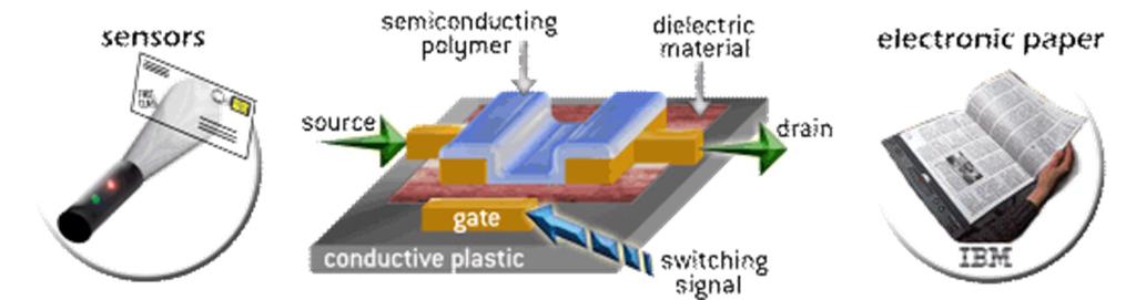
20 molecular orbitals (MO) of aromatic molecules: Benzol
21 Naming orbitals: HOMO and LUMO
22 Nobel Price Chemistry 2000: Alan J. Heeger
23 Doped polymers are conducting: PDOT : PSS poly(styrenesulfonate),


24 Nobel prices for aromatic and conjugated materials Graphene 2010 physics Polyacetylene 2000 chemistry Fullerenes 1996 chemistry
25
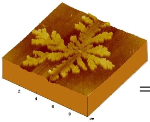
26
27 Linear acenes: HOMO LUMO band gap Bsp. Pentacene: Absorption
28 Translation valence band, conduction band, electron-hole pair, doping, traps for charge carriers, phonons, energy bands, Drude model, electroluminescence, surface states LUMO, HOMO, excitonic states, chemical impurities, vibrations, hopping, fluorescence and phosphorescence, singulets, triplets, anhilation, oxidation, reduction


29 The vision of organic electronics: mass printing
30 Status Quo... 90% of OLEDs, by far the most important application of organic electronics at the moment, are produced by vapor deposition of small molecules [Source: ICB 10 July 2008 ]
31 Organic materials deposition and growth
32 Record material: Pentacene C22H14 Properties: hole mobility larger than electron mobility forms well-ordered layers when evaporated in vacuum at RT gold contact are reasonably well matched


33 Pentacene-deposition by vacuum sublimation, accuracy ca. 0.1 nm (QMC)


34 Pentacene film growth H H H H H H Si OH OH OH OH OH OH SiO 2 Si mm 10 mm Phys. Rev. B (2003)
35 Diffusion limited Aggregation (DLA) diffusion nucleation surface modification = Diffusionsenergie = Diffusionskonstante temperature deposition rate island formation R = D / F

36 Molecular structure: Bragg-scattering APL (2004)

")
37 Pentacene growth (thick films)


38 Comparison: Coronene films 1.5µm 3µm M. Huth (LMU), diploma thesis (2006)


39 surface energy determines growth mode (Wulf construction)
40
41 Summary: Deposition and structure Growth mode of small molecules largely determined by molecular shape and surface energy molecular arrangement can be determined by x-ray experiments
42 Carrier mobility


43
44 little overlap - bands are flat mass of the carriers is high mobility is low scattering time depends on sample quality
 Charge carriers are generated at the surface due to adsorption 2.")
45 Measurement of mobility: Time-Of-Flight: Kepler & LeBlanc 1960 for Anthracene crystals TOF-Geometry 1. Generation of elektron-eole pairs by hard light pulse ( pulse 0.76ns) Charge carriers are generated at the surface due to adsorption 2. measurement of displacement current Experiment injection free method electron and hole current separately

46 typical mobility for organics m = 1 cm 2 /Vs same as amorphous Si
47 traps reduce mobility (Shockley-Read-Hall) µ 0 (T): intrinsic mobility E T : trap energy N T /N 0 : trapping vs. conduction states mobility, in the presence of shallow traps: m(t) = where m 0 (T) ~ T -n N T m 0 (T) 1 + [exp( ) -1] N 0 E T k B T n depending on material, scattering mechanisms, etc.
48 grain boundaries reduce mobility Horowitz Adv. Mat. (2000)
![Comparison of organic and inorganic Semiconductors E [ev] 0 E vac narrow bands ( ca. 100meV at 300K ) 2.2 E gap E cb high mass E F 5.](/docs-images/88/115901702/images/49-0.jpg "8 E vb x bandgap E gap 3.6eV (diamond E gap = 5.")
49 Comparison of organic and inorganic Semiconductors E [ev] 0 E vac narrow bands ( ca. 100meV at 300K ) 2.2 E gap E cb high mass E F 5.8 E vb x bandgap E gap 3.6eV (diamond E gap = 5.5eV) k B T = 26meV at 300K Compared to tetracene: no free carriers in thermal equilibrium strong influence of traps
50 Summary electronic properties conjugated and aromatic molecules have delocalized electrons (p electrons) small organic molecules form highly ordered crystals, while polymer films are only partially ordered Details of the arrangement of the molecular orbitals and symmetry determine the electronic properties of organic crystals organic molecules have large band gaps (typically 2 ev), few or no intrinsic carriers at RT bands are flat, dispersion typically 100 mev crystal quality matters for mobility (grain boundaries, traps)
51 Thin-film devices transistors p-n contacts (diodes, solar cells, oleds)
52 Thin film transistors
( C ox 1.")
 200 µm 250 µm")

53 Thin film transistors - design -8 2 Thermal SiO 2 (200nm)( C ox F / cm ) ~ 48 nm Pentacene Gold-structure(bottom-contact) 200 µm 250 µm 750 µm Contacts (60 nm Au + 3nm Ti) w = 10 µm l = 20 µm Channel Transistor channel Pentacene on SiO µm 2.5 µm 25 µm 5 µm
54 Field effect-transistors from pentacene molecules
55 Organic field effect transistors (see blackboard for characteristic curve) Precise saturation behaviour Linear regime I SD * 10-5 [A] V G = 0 V V G = -10 V V G = -20 V V G = -30 V Ohmic contacts V SD [V] p-type pentacene bottom-contact OTFTs
56 Pentacene TFTs : trap density 1st measurement last measurement Threshold shift V T deep traps Energy level far from HOMO level Fixed interface charges Hysteresis V shallow traps Energy level near HOMO level Can be released thermally ID 0099: ID 0099: M. Fiebig (LMU, LS Kotthaus), Diploma thesis 2005
57 Diodes, solar cells
58 Optical excitations in organic crystals Singlet excitons diffuse within the organic crystal until they decay fluorescent or radiationless. Lifetime is very short (fs-ps), therefore diffusion length is only nm.


59 Si the p/n- junction energy band deformation by doping


60 Exciton splitting at hetero-junctions Appl. Phys. Lett. 48, 183 (1986) Two layer organic photovoltaic cell C. W. Tang Modellsystem: Pentacene/C60 (C60 erst ab 1985 bekannt) p n

61 Organic solar cells e h
62 Summary active elements (diode, transistor) made from organic electronics materials: OLEDs, solar cells, field-effect-transistors (FETs) materials science aspects have huge influence on performance: structural defects, chemical impurities, lifetime and stability need to be optimized the molecular character is usually not completely lost in crystals: strongly bound excitons, low epsilon
63 Organic Electronics summer term 18 Pentacene Linear Acenes:
64 Comparison Pentacene-Gold MOSFET Metal-Oxide-Semiconductor field-effect-transistor here: p-type, normally off similar: MISFET (metal insulator...) IGFET (insulator-gate...)
65 working principle of an OFET plate capacitor gate electrode contact + semicond. film
66 I-V curve of a MOSFET conceptionally, L>>d (channel length >> oxide thickness) Moors law requires thin oxides as main technological challenge for small MosFETS with Si with organic FETs, parasitic problems dominate so far: contact barriers, traps, contaminations,...
67 linear range: amplifier saturation regime: logic
68
Semiconductor Polymer
 Semiconductor Polymer Organic Semiconductor for Flexible Electronics Introduction: An organic semiconductor is an organic compound that possesses similar properties to inorganic semiconductors with hole
Organic Electronic Devices
 Organic Electronic Devices Week 5: Organic Light-Emitting Devices and Emerging Technologies Lecture 5.5: Course Review and Summary Bryan W. Boudouris Chemical Engineering Purdue University 1 Understanding
Basic cell design. Si cell
 Basic cell design Si cell 1 Concepts needed to describe photovoltaic device 1. energy bands in semiconductors: from bonds to bands 2. free carriers: holes and electrons, doping 3. electron and hole current:
1 Name: Student number: DEPARTMENT OF PHYSICS AND PHYSICAL OCEANOGRAPHY MEMORIAL UNIVERSITY OF NEWFOUNDLAND. Fall :00-11:00
 1 Name: DEPARTMENT OF PHYSICS AND PHYSICAL OCEANOGRAPHY MEMORIAL UNIVERSITY OF NEWFOUNDLAND Final Exam Physics 3000 December 11, 2012 Fall 2012 9:00-11:00 INSTRUCTIONS: 1. Answer all seven (7) questions.
Plastic Electronics. Joaquim Puigdollers.
 Plastic Electronics Joaquim Puigdollers Joaquim.puigdollers@upc.edu Nobel Prize Chemistry 2000 Origins Technological Interest First products.. MONOCROMATIC PHILIPS Today Future Technological interest Low
Organic Device Simulation Using Silvaco Software. Silvaco Taiwan September 2005
 Organic Device Simulation Using Silvaco Software Silvaco Taiwan September 2005 Organic Devices Simulation: Contents Introduction Silvaco TCAD Simulator Theory Models OTFT Simulation v.s Measurement OLED
Photovoltaics. Lecture 7 Organic Thin Film Solar Cells Photonics - Spring 2017 dr inż. Aleksander Urbaniak
 Photovoltaics Lecture 7 Organic Thin Film Solar Cells Photonics - Spring 2017 dr inż. Aleksander Urbaniak Barcelona, Spain Perpignan train station, France source: pinterest Why organic solar cells? 1.
Physics of Organic Semiconductor Devices: Materials, Fundamentals, Technologies and Applications
 Physics of Organic Semiconductor Devices: Materials, Fundamentals, Technologies and Applications Dr. Alex Zakhidov Assistant Professor, Physics Department Core faculty at Materials Science, Engineering
ESE370: Circuit-Level Modeling, Design, and Optimization for Digital Systems
 ESE370: Circuit-Level Modeling, Design, and Optimization for Digital Systems Lec 6: September 14, 2015 MOS Model You are Here: Transistor Edition! Previously: simple models (0 and 1 st order) " Comfortable
Quiz #1 Practice Problem Set
 Name: Student Number: ELEC 3908 Physical Electronics Quiz #1 Practice Problem Set? Minutes January 22, 2016 - No aids except a non-programmable calculator - All questions must be answered - All questions
Mesoporous titanium dioxide electrolyte bulk heterojunction
 Mesoporous titanium dioxide electrolyte bulk heterojunction The term "bulk heterojunction" is used to describe a heterojunction composed of two different materials acting as electron- and a hole- transporters,
EE130: Integrated Circuit Devices
 EE130: Integrated Circuit Devices (online at http://webcast.berkeley.edu) Instructor: Prof. Tsu-Jae King (tking@eecs.berkeley.edu) TA s: Marie Eyoum (meyoum@eecs.berkeley.edu) Alvaro Padilla (apadilla@eecs.berkeley.edu)
ELECTRONIC DEVICES AND CIRCUITS SUMMARY
 ELECTRONIC DEVICES AND CIRCUITS SUMMARY Classification of Materials: Insulator: An insulator is a material that offers a very low level (or negligible) of conductivity when voltage is applied. Eg: Paper,
Classification of Solids
 Classification of Solids Classification by conductivity, which is related to the band structure: (Filled bands are shown dark; D(E) = Density of states) Class Electron Density Density of States D(E) Examples
Enhanced Optical and Electrical Properties of Organic Field Effect Transistor using Metal Nanoparticles
 University of Miami Scholarly Repository Open Access Theses Electronic Theses and Dissertations 2014-07-28 Enhanced Optical and Electrical Properties of Organic Field Effect Transistor using Metal Nanoparticles
Surfaces, Interfaces, and Layered Devices
 Surfaces, Interfaces, and Layered Devices Building blocks for nanodevices! W. Pauli: God made solids, but surfaces were the work of Devil. Surfaces and Interfaces 1 Interface between a crystal and vacuum
Semiconductor Physical Electronics
 Semiconductor Physical Electronics Sheng S. Li Department of Electrical Engineering University of Florida Gainesville, Florida Plenum Press New York and London Contents CHAPTER 1. Classification of Solids
3.1 Introduction to Semiconductors. Y. Baghzouz ECE Department UNLV
 3.1 Introduction to Semiconductors Y. Baghzouz ECE Department UNLV Introduction In this lecture, we will cover the basic aspects of semiconductor materials, and the physical mechanisms which are at the
Sheng S. Li. Semiconductor Physical Electronics. Second Edition. With 230 Figures. 4) Springer
 Springer") Sheng S. Li Semiconductor Physical Electronics Second Edition With 230 Figures 4) Springer Contents Preface 1. Classification of Solids and Crystal Structure 1 1.1 Introduction 1 1.2 The Bravais Lattice
Sheng S. Li Semiconductor Physical Electronics Second Edition With 230 Figures 4) Springer Contents Preface 1. Classification of Solids and Crystal Structure 1 1.1 Introduction 1 1.2 The Bravais Lattice
Fabrication Technology, Part I
 EEL5225: Principles of MEMS Transducers (Fall 2004) Fabrication Technology, Part I Agenda: Microfabrication Overview Basic semiconductor devices Materials Key processes Oxidation Thin-film Deposition Reading:
Halbleiter Prof. Yong Lei Prof. Thomas Hannappel
 Halbleiter Prof. Yong Lei Prof. Thomas Hannappel yong.lei@tu-ilmenau.de thomas.hannappel@tu-ilmenau.de http://www.tu-ilmenau.de/nanostruk/ Organic Semiconductors & Organic Electronics Organic semiconductors
Energetic particles and their detection in situ (particle detectors) Part II. George Gloeckler
 Part II. George Gloeckler") Energetic particles and their detection in situ (particle detectors) Part II George Gloeckler University of Michigan, Ann Arbor, MI University of Maryland, College Park, MD Simple particle detectors Gas-filled
Energetic particles and their detection in situ (particle detectors) Part II George Gloeckler University of Michigan, Ann Arbor, MI University of Maryland, College Park, MD Simple particle detectors Gas-filled
ESE370: Circuit-Level Modeling, Design, and Optimization for Digital Systems
 ESE370: Circuit-Level Modeling, Design, and Optimization for Digital Systems Lec 6: September 18, 2017 MOS Model You are Here: Transistor Edition! Previously: simple models (0 and 1 st order) " Comfortable
Organic solar cells. State of the art and outlooks. Gilles Horowitz LPICM, UMR7647 CNRS - Ecole Polytechnique
 Organic solar cells. State of the art and outlooks Gilles Horowitz LPICM, UMR7647 CNRS - Ecole Polytechnique Solar energy Solar energy on earth: 75,000 tep/year 6000 times the world consumption in 2007
PHOTOVOLTAICS Fundamentals
 PHOTOVOLTAICS Fundamentals PV FUNDAMENTALS Semiconductor basics pn junction Solar cell operation Design of silicon solar cell SEMICONDUCTOR BASICS Allowed energy bands Valence and conduction band Fermi
Lecture 7: Extrinsic semiconductors - Fermi level
 Lecture 7: Extrinsic semiconductors - Fermi level Contents 1 Dopant materials 1 2 E F in extrinsic semiconductors 5 3 Temperature dependence of carrier concentration 6 3.1 Low temperature regime (T < T
Lecture 2. Introduction to semiconductors Structures and characteristics in semiconductors
 Lecture 2 Introduction to semiconductors Structures and characteristics in semiconductors Semiconductor p-n junction Metal Oxide Silicon structure Semiconductor contact Literature Glen F. Knoll, Radiation
Solid State Device Fundamentals
 Solid State Device Fundamentals ENS 345 Lecture Course by Alexander M. Zaitsev alexander.zaitsev@csi.cuny.edu Tel: 718 982 2812 Office 4N101b 1 Outline - Goals of the course. What is electronic device?
Electronics The basics of semiconductor physics
 Electronics The basics of semiconductor physics Prof. Márta Rencz, Gergely Nagy BME DED September 16, 2013 The basic properties of semiconductors Semiconductors conductance is between that of conductors
! Previously: simple models (0 and 1 st order) " Comfortable with basic functions and circuits. ! This week and next (4 lectures)
 Comfortable with basic functions and circuits. ! This week and next (4 lectures)") ESE370: CircuitLevel Modeling, Design, and Optimization for Digital Systems Lec 6: September 14, 2015 MOS Model You are Here: Transistor Edition! Previously: simple models (0 and 1 st order) " Comfortable
ESE370: CircuitLevel Modeling, Design, and Optimization for Digital Systems Lec 6: September 14, 2015 MOS Model You are Here: Transistor Edition! Previously: simple models (0 and 1 st order) " Comfortable
Organic Molecular Solids
 Markus Schwoerer, Hans Christoph Wolf Organic Molecular Solids BICENTENNIAL BICENTENNIAL WILEY-VCH Verlag GmbH & Co. KGaA VII Contents 1 Introduction 1 1.1 What are Organic Solids? 1 1.2 What are the Special
Supporting Information
 Supporting Information Oh et al. 10.1073/pnas.0811923106 SI Text Hysteresis of BPE-PTCDI MW-TFTs. Fig. S9 represents bidirectional transfer plots at V DS 100VinN 2 atmosphere for transistors constructed
GaN based transistors
 GaN based transistors S FP FP dielectric G SiO 2 Al x Ga 1-x N barrier i-gan Buffer i-sic D Transistors "The Transistor was probably the most important invention of the 20th Century The American Institute
Flexible Organic Photovoltaics Employ laser produced metal nanoparticles into the absorption layer 1. An Introduction
 Flexible Organic Photovoltaics Employ laser produced metal nanoparticles into the absorption layer 1. An Introduction Among the renewable energy sources that are called to satisfy the continuously increased
Chapter 4: Bonding in Solids and Electronic Properties. Free electron theory
 Chapter 4: Bonding in Solids and Electronic Properties Free electron theory Consider free electrons in a metal an electron gas. regards a metal as a box in which electrons are free to move. assumes nuclei
Chemistry Instrumental Analysis Lecture 8. Chem 4631
 Chemistry 4631 Instrumental Analysis Lecture 8 UV to IR Components of Optical Basic components of spectroscopic instruments: stable source of radiant energy transparent container to hold sample device
ESE370: Circuit-Level Modeling, Design, and Optimization for Digital Systems. Today MOS MOS. Capacitor. Idea
 ESE370: Circuit-Level Modeling, Design, and Optimization for Digital Systems Day 9: September 26, 2011 MOS Model Today MOS Structure Basic Idea Semiconductor Physics Metals, insulators Silicon lattice
ET3034TUx Utilization of band gap energy
 ET3034TUx - 3.3.1 - Utilization of band gap energy In the last two weeks we have discussed the working principle of a solar cell and the external parameters that define the performance of a solar cell.
Final Examination EE 130 December 16, 1997 Time allotted: 180 minutes
 Final Examination EE 130 December 16, 1997 Time allotted: 180 minutes Problem 1: Semiconductor Fundamentals [30 points] A uniformly doped silicon sample of length 100µm and cross-sectional area 100µm 2
Initial Stages of Growth of Organic Semiconductors on Graphene
 Initial Stages of Growth of Organic Semiconductors on Graphene Presented by: Manisha Chhikara Supervisor: Prof. Dr. Gvido Bratina University of Nova Gorica Outline Introduction to Graphene Fabrication
Semiconductors and Optoelectronics. Today Semiconductors Acoustics. Tomorrow Come to CH325 Exercises Tours
 Semiconductors and Optoelectronics Advanced Physics Lab, PHYS 3600 Don Heiman, Northeastern University, 2017 Today Semiconductors Acoustics Tomorrow Come to CH325 Exercises Tours Semiconductors and Optoelectronics
Enhancing the Performance of Organic Thin-Film Transistor using a Buffer Layer
 Proceedings of the 9th International Conference on Properties and Applications of Dielectric Materials July 19-23, 29, Harbin, China L-7 Enhancing the Performance of Organic Thin-Film Transistor using
Section 12: Intro to Devices
 Section 12: Intro to Devices Extensive reading materials on reserve, including Robert F. Pierret, Semiconductor Device Fundamentals EE143 Ali Javey Bond Model of Electrons and Holes Si Si Si Si Si Si Si
Theory of Electrical Characterization of Semiconductors
 Theory of Electrical Characterization of Semiconductors P. Stallinga Universidade do Algarve U.C.E.H. A.D.E.E.C. OptoElectronics SELOA Summer School May 2000, Bologna (It) Overview Devices: bulk Schottky
R. Ludwig and G. Bogdanov RF Circuit Design: Theory and Applications 2 nd edition. Figures for Chapter 6
 R. Ludwig and G. Bogdanov RF Circuit Design: Theory and Applications 2 nd edition Figures for Chapter 6 Free electron Conduction band Hole W g W C Forbidden Band or Bandgap W V Electron energy Hole Valence
Section 12: Intro to Devices
 Section 12: Intro to Devices Extensive reading materials on reserve, including Robert F. Pierret, Semiconductor Device Fundamentals Bond Model of Electrons and Holes Si Si Si Si Si Si Si Si Si Silicon
ELEMENTARY BAND THEORY
 ELEMENTARY BAND THEORY PHYSICIST Solid state band Valence band, VB Conduction band, CB Fermi energy, E F Bloch orbital, delocalized n-doping p-doping Band gap, E g Direct band gap Indirect band gap Phonon
EE143 Fall 2016 Microfabrication Technologies. Evolution of Devices
 EE143 Fall 2016 Microfabrication Technologies Prof. Ming C. Wu wu@eecs.berkeley.edu 511 Sutardja Dai Hall (SDH) 1-1 Evolution of Devices Yesterday s Transistor (1947) Today s Transistor (2006) 1-2 1 Why
! Previously: simple models (0 and 1 st order) " Comfortable with basic functions and circuits. ! This week and next (4 lectures)
 Comfortable with basic functions and circuits. ! This week and next (4 lectures)") ESE370: CircuitLevel Modeling, Design, and Optimization for Digital Systems Lec 6: September 18, 2017 MOS Model You are Here: Transistor Edition! Previously: simple models (0 and 1 st order) " Comfortable
ESE370: CircuitLevel Modeling, Design, and Optimization for Digital Systems Lec 6: September 18, 2017 MOS Model You are Here: Transistor Edition! Previously: simple models (0 and 1 st order) " Comfortable
Solid State Device Fundamentals
 Solid State Device Fundamentals ENS 345 Lecture Course by Alexander M. Zaitsev alexander.zaitsev@csi.cuny.edu Tel: 718 982 2812 Office 4N101b 1 Outline - Goals of the course. What is electronic device?
an introduction to Semiconductor Devices
 an introduction to Semiconductor Devices Donald A. Neamen Chapter 6 Fundamentals of the Metal-Oxide-Semiconductor Field-Effect Transistor Introduction: Chapter 6 1. MOSFET Structure 2. MOS Capacitor -
Semiconductor device structures are traditionally divided into homojunction devices
 0. Introduction: Semiconductor device structures are traditionally divided into homojunction devices (devices consisting of only one type of semiconductor material) and heterojunction devices (consisting
EECS143 Microfabrication Technology
 EECS143 Microfabrication Technology Professor Ali Javey Introduction to Materials Lecture 1 Evolution of Devices Yesterday s Transistor (1947) Today s Transistor (2006) Why Semiconductors? Conductors e.g
CHARGE CARRIERS PHOTOGENERATION. Maddalena Binda Organic Electronics: principles, devices and applications Milano, November 23-27th, 2015
 CHARGE CARRIERS PHOTOGENERATION Maddalena Binda Organic Electronics: principles, devices and applications Milano, November 23-27th, 2015 Charge carriers photogeneration: what does it mean? Light stimulus
Electrons are shared in covalent bonds between atoms of Si. A bound electron has the lowest energy state.
 Photovoltaics Basic Steps the generation of light-generated carriers; the collection of the light-generated carriers to generate a current; the generation of a large voltage across the solar cell; and
Structure Property Relationships of. Organic Light-Emitting Diodes. Michael Kochanek May 19, 2006 MS&E 542 Flexible Electronics
 Structure Property Relationships of Organic Light-Emitting Diodes Michael Kochanek May 19, 2006 MS&E 542 Flexible Electronics Introduction Many of today s solid-state inorganic microelectronic devices
The Study of Charge Carrier Transports in the Calamitic Liquid Crystals 5, 5 -di-(decyl-pyridin-yl) - 2 Bithiophene.
 - 2 Bithiophene.") The Study of Charge Carrier Transports in the Calamitic Liquid Crystals 5, 5 -di-(decyl-pyridin-yl) - 2 Bithiophene Naresh Shakya * C. Pokhrel* and B. Ellman* Y. Getmanenko** and R. J. Twieg** *Department
The Study of Charge Carrier Transports in the Calamitic Liquid Crystals 5, 5 -di-(decyl-pyridin-yl) - 2 Bithiophene Naresh Shakya * C. Pokhrel* and B. Ellman* Y. Getmanenko** and R. J. Twieg** *Department
Conductivity and Semi-Conductors
 Conductivity and Semi-Conductors J = current density = I/A E = Electric field intensity = V/l where l is the distance between two points Metals: Semiconductors: Many Polymers and Glasses 1 Electrical Conduction
CME 300 Properties of Materials. ANSWERS: Homework 9 November 26, As atoms approach each other in the solid state the quantized energy states:
 CME 300 Properties of Materials ANSWERS: Homework 9 November 26, 2011 As atoms approach each other in the solid state the quantized energy states: are split. This splitting is associated with the wave
Electron Energy, E E = 0. Free electron. 3s Band 2p Band Overlapping energy bands. 3p 3s 2p 2s. 2s Band. Electrons. 1s ATOM SOLID.
 Electron Energy, E Free electron Vacuum level 3p 3s 2p 2s 2s Band 3s Band 2p Band Overlapping energy bands Electrons E = 0 1s ATOM 1s SOLID In a metal the various energy bands overlap to give a single
MENA9510 characterization course: Capacitance-voltage (CV) measurements
 measurements") MENA9510 characterization course: Capacitance-voltage (CV) measurements 30.10.2017 Halvard Haug Outline Overview of interesting sample structures Ohmic and schottky contacts Why C-V for solar cells? The
MENA9510 characterization course: Capacitance-voltage (CV) measurements 30.10.2017 Halvard Haug Outline Overview of interesting sample structures Ohmic and schottky contacts Why C-V for solar cells? The
Lecture 1. OUTLINE Basic Semiconductor Physics. Reading: Chapter 2.1. Semiconductors Intrinsic (undoped) silicon Doping Carrier concentrations
 silicon Doping Carrier concentrations") Lecture 1 OUTLINE Basic Semiconductor Physics Semiconductors Intrinsic (undoped) silicon Doping Carrier concentrations Reading: Chapter 2.1 EE105 Fall 2007 Lecture 1, Slide 1 What is a Semiconductor? Low
Lecture 1 OUTLINE Basic Semiconductor Physics Semiconductors Intrinsic (undoped) silicon Doping Carrier concentrations Reading: Chapter 2.1 EE105 Fall 2007 Lecture 1, Slide 1 What is a Semiconductor? Low
EECS130 Integrated Circuit Devices
 EECS130 Integrated Circuit Devices Professor Ali Javey 10/02/2007 MS Junctions, Lecture 2 MOS Cap, Lecture 1 Reading: finish chapter14, start chapter16 Announcements Professor Javey will hold his OH at
Molecular Electronics For Fun and Profit(?)
") Molecular Electronics For Fun and Profit(?) Prof. Geoffrey Hutchison Department of Chemistry University of Pittsburgh geoffh@pitt.edu July 22, 2009 http://hutchison.chem.pitt.edu Moore s Law: Transistor
Molecular Electronics For Fun and Profit(?) Prof. Geoffrey Hutchison Department of Chemistry University of Pittsburgh geoffh@pitt.edu July 22, 2009 http://hutchison.chem.pitt.edu Moore s Law: Transistor
Electronics with 2D Crystals: Scaling extender, or harbinger of new functions?
 Electronics with 2D Crystals: Scaling extender, or harbinger of new functions? 1 st Workshop on Data Abundant Systems Technology Stanford, April 2014 Debdeep Jena (djena@nd.edu) Electrical Engineering,
Surfaces, Interfaces, and Layered Devices
 Surfaces, Interfaces, and Layered Devices Building blocks for nanodevices! W. Pauli: God made solids, but surfaces were the work of Devil. Surfaces and Interfaces 1 Role of surface effects in mesoscopic
Introduction to Semiconductor Physics. Prof.P. Ravindran, Department of Physics, Central University of Tamil Nadu, India
 Introduction to Semiconductor Physics 1 Prof.P. Ravindran, Department of Physics, Central University of Tamil Nadu, India http://folk.uio.no/ravi/cmp2013 Review of Semiconductor Physics Semiconductor fundamentals
Lecture 12: MOS Capacitors, transistors. Context
 Lecture 12: MOS Capacitors, transistors Context In the last lecture, we discussed PN diodes, and the depletion layer into semiconductor surfaces. Small signal models In this lecture, we will apply those
Triplet state diffusion in organometallic and organic semiconductors
 Triplet state diffusion in organometallic and organic semiconductors Prof. Anna Köhler Experimental Physik II University of Bayreuth Germany From materials properties To device applications Organic semiconductors
SEMICONDUCTOR PHYSICS REVIEW BONDS,
 SEMICONDUCTOR PHYSICS REVIEW BONDS, BANDS, EFFECTIVE MASS, DRIFT, DIFFUSION, GENERATION, RECOMBINATION February 3, 2011 The University of Toledo, Department of Physics and Astronomy SSARE, PVIC Principles
Lecture 2. Introduction to semiconductors Structures and characteristics in semiconductors
 Lecture 2 Introduction to semiconductors Structures and characteristics in semiconductors Semiconductor p-n junction Metal Oxide Silicon structure Semiconductor contact Literature Glen F. Knoll, Radiation
Semiconductor Detectors
 Semiconductor Detectors Summary of Last Lecture Band structure in Solids: Conduction band Conduction band thermal conductivity: E g > 5 ev Valence band Insulator Charge carrier in conductor: e - Charge
Sébastien FORGET. Laboratoire de Physique des Lasers Université Paris Nord P13. www-lpl.univ-paris13.fr:8088/lumen/
 OLEDs Basic principles, technology and applications Sébastien FORGET Laboratoire de Physique des Lasers Université Paris Nord P13 www-lpl.univ-paris13.fr:8088/lumen/ Paris Nord University (Paris 13) This
ORGANIC SEMICONDUCTOR 3,4,9,10-Perylenetetracarboxylic dianhydride (PTCDA)
") ORGANIC SEMICONDUCTOR 3,4,9,10-Perylenetetracarboxylic dianhydride (PTCDA) Suvranta Tripathy Department of Physics University of Cincinnati Cincinnati, Ohio 45221 March 8, 2002 Abstract In the last decade
ORGANIC SEMICONDUCTOR 3,4,9,10-Perylenetetracarboxylic dianhydride (PTCDA) Suvranta Tripathy Department of Physics University of Cincinnati Cincinnati, Ohio 45221 March 8, 2002 Abstract In the last decade
Fundamentals of the Metal Oxide Semiconductor Field-Effect Transistor
 Triode Working FET Fundamentals of the Metal Oxide Semiconductor Field-Effect Transistor The characteristics of energy bands as a function of applied voltage. Surface inversion. The expression for the
Calculating Band Structure
 Calculating Band Structure Nearly free electron Assume plane wave solution for electrons Weak potential V(x) Brillouin zone edge Tight binding method Electrons in local atomic states (bound states) Interatomic
Unit IV Semiconductors Engineering Physics
 Introduction A semiconductor is a material that has a resistivity lies between that of a conductor and an insulator. The conductivity of a semiconductor material can be varied under an external electrical
Current mechanisms Exam January 27, 2012
 Current mechanisms Exam January 27, 2012 There are four mechanisms that typically cause currents to flow: thermionic emission, diffusion, drift, and tunneling. Explain briefly which kind of current mechanisms
Electrostatics of Nanowire Transistors
 Electrostatics of Nanowire Transistors Jing Guo, Jing Wang, Eric Polizzi, Supriyo Datta and Mark Lundstrom School of Electrical and Computer Engineering Purdue University, West Lafayette, IN, 47907 ABSTRACTS
Semiconductor-Detectors
 Semiconductor-Detectors 1 Motivation ~ 195: Discovery that pn-- junctions can be used to detect particles. Semiconductor detectors used for energy measurements ( Germanium) Since ~ 3 years: Semiconductor
Dynamics and Structure-Property Relationships in Organic Single Crystal Electrical Double Layer Transistors
 Dynamics and Structure-Property Relationships in Organic Single Crystal Electrical Double Layer Transistors A Dissertation SUBMITTED TO THE FACULTY OF UNIVERSITY OF MINNESOTA BY Elliot Schmidt IN PARTIAL
Lecture 1. Introduction to Electronic Materials. Reading: Pierret 1.1, 1.2, 1.4,
 Lecture 1 Introduction to Electronic Materials Reading: Pierret 1.1, 1.2, 1.4, 2.1-2.6 Atoms to Operational Amplifiers The goal of this course is to teach the fundamentals of non-linear circuit elements
Lecture 2. Introduction to semiconductors Structures and characteristics in semiconductors. Fabrication of semiconductor sensor
 Lecture 2 Introduction to semiconductors Structures and characteristics in semiconductors Semiconductor p-n junction Metal Oxide Silicon structure Semiconductor contact Fabrication of semiconductor sensor
Resonant photo-ionization of point defects in HfO 2 thin films observed by second-harmonic generation.
 Optics of Surfaces & Interfaces - VIII September 10 th, 2009 Resonant photo-ionization of point defects in HfO 2 thin films observed by second-harmonic generation. Jimmy Price and Michael C. Downer Physics
Crystal Properties. MS415 Lec. 2. High performance, high current. ZnO. GaN
 Crystal Properties Crystal Lattices: Periodic arrangement of atoms Repeated unit cells (solid-state) Stuffing atoms into unit cells Determine mechanical & electrical properties High performance, high current
How does a polymer LED OPERATE?
 How does a polymer LED OPERATE? Now that we have covered many basic issues we can try and put together a few concepts as they appear in a working device. We start with an LED:. Charge injection a. Hole
KATIHAL FİZİĞİ MNT-510
 KATIHAL FİZİĞİ MNT-510 YARIİLETKENLER Kaynaklar: Katıhal Fiziği, Prof. Dr. Mustafa Dikici, Seçkin Yayıncılık Katıhal Fiziği, Şakir Aydoğan, Nobel Yayıncılık, Physics for Computer Science Students: With
ECE 340 Lecture 39 : MOS Capacitor II
 ECE 340 Lecture 39 : MOS Capacitor II Class Outline: Effects of Real Surfaces Threshold Voltage MOS Capacitance-Voltage Analysis Things you should know when you leave Key Questions What are the effects
Microwave Absorption by Light-induced Free Carriers in Silicon
 Microwave Asorption y Light-induced Free Carriers in Silicon T. Sameshima and T. Haa Tokyo University of Agriculture and Technology, Koganei, Tokyo 184-8588, Japan E-mail address: tsamesim@cc.tuat.ac.jp
Stretching the Barriers An analysis of MOSFET Scaling. Presenters (in order) Zeinab Mousavi Stephanie Teich-McGoldrick Aseem Jain Jaspreet Wadhwa
 Zeinab Mousavi Stephanie Teich-McGoldrick Aseem Jain Jaspreet Wadhwa") Stretching the Barriers An analysis of MOSFET Scaling Presenters (in order) Zeinab Mousavi Stephanie Teich-McGoldrick Aseem Jain Jaspreet Wadhwa Why Small? Higher Current Lower Gate Capacitance Higher
Stretching the Barriers An analysis of MOSFET Scaling Presenters (in order) Zeinab Mousavi Stephanie Teich-McGoldrick Aseem Jain Jaspreet Wadhwa Why Small? Higher Current Lower Gate Capacitance Higher
A. OTHER JUNCTIONS B. SEMICONDUCTOR HETEROJUNCTIONS -- MOLECULES AT INTERFACES: ORGANIC PHOTOVOLTAIC BULK HETEROJUNCTION DYE-SENSITIZED SOLAR CELL
 A. OTHER JUNCTIONS B. SEMICONDUCTOR HETEROJUNCTIONS -- MOLECULES AT INTERFACES: ORGANIC PHOTOVOLTAIC BULK HETEROJUNCTION DYE-SENSITIZED SOLAR CELL March 24, 2015 The University of Toledo, Department of
Chapter 12: Electrical Properties. RA l
 Charge carriers and conduction: Chapter 12: Electrical Properties Charge carriers include all species capable of transporting electrical charge, including electrons, ions, and electron holes. The latter
(a) (b) Supplementary Figure 1. (a) (b) (a) Supplementary Figure 2. (a) (b) (c) (d) (e)
 (b) Supplementary Figure 1. (a) (b) (a) Supplementary Figure 2. (a) (b) (c) (d) (e)") (a) (b) Supplementary Figure 1. (a) An AFM image of the device after the formation of the contact electrodes and the top gate dielectric Al 2 O 3. (b) A line scan performed along the white dashed line
(a) (b) Supplementary Figure 1. (a) An AFM image of the device after the formation of the contact electrodes and the top gate dielectric Al 2 O 3. (b) A line scan performed along the white dashed line
ESE 372 / Spring 2013 / Lecture 5 Metal Oxide Semiconductor Field Effect Transistor
 Metal Oxide Semiconductor Field Effect Transistor V G V G 1 Metal Oxide Semiconductor Field Effect Transistor We will need to understand how this current flows through Si What is electric current? 2 Back
Semiconductor Device Physics
 1 Semiconductor Device Physics Lecture 1 http://zitompul.wordpress.com 2 0 1 3 2 Semiconductor Device Physics Textbook: Semiconductor Device Fundamentals, Robert F. Pierret, International Edition, Addison
MTLE-6120: Advanced Electronic Properties of Materials. Intrinsic and extrinsic semiconductors. Reading: Kasap:
 MTLE-6120: Advanced Electronic Properties of Materials 1 Intrinsic and extrinsic semiconductors Reading: Kasap: 5.1-5.6 Band structure and conduction 2 Metals: partially filled band(s) i.e. bands cross
Electronic Devices & Circuits
 Electronic Devices & Circuits For Electronics & Communication Engineering By www.thegateacademy.com Syllabus Syllabus for Electronic Devices Energy Bands in Intrinsic and Extrinsic Silicon, Carrier Transport,
Observation of electron injection in an organic field-effect transistor with electroluminescence *
 Materials Science-Poland, Vol. 27, No. 3, 2009 Observation of electron injection in an organic field-effect transistor with electroluminescence * Y. OHSHIMA **, H. KOHN, E. LIM, T. MANAKA, M. IWAMOTO Department
Appendix 1: List of symbols
 Appendix 1: List of symbols Symbol Description MKS Units a Acceleration m/s 2 a 0 Bohr radius m A Area m 2 A* Richardson constant m/s A C Collector area m 2 A E Emitter area m 2 b Bimolecular recombination
High Performance, Low Operating Voltage n-type Organic Field Effect Transistor Based on Inorganic-Organic Bilayer Dielectric System
 Journal of Physics: Conference Series PAPER OPEN ACCESS High Performance, Low Operating Voltage n-type Organic Field Effect Transistor Based on Inorganic-Organic Bilayer Dielectric System To cite this