Self-assembly and Nanotechnology
|
|
|
- Lindsay West
- 5 years ago
- Views:
Transcription
1 Self-assembly and Nanotechnology Instructor: Dr. Zhiyong Gu Office: Perry Hall 222 Office Phone: Office hours: Mon 11:00am-12:30pm; Office hours: Mon 11:00am-12:30pm; Wed 11:00am-12:30pm, and by appointment
2 Why Together? Self-assembly Nanotechnology Self-assembly and Nanotechnology
3 What s Nanotechnology?????? Nanomaterials Nanoscience Nanoengineering i Nanotechnology Nanomanufacturing Nano-xxxxxxx Your answers Nanotechnology is the understanding and control of matter at dimensions of roughly 1 to 100 nanometers, where unique phenomena enable novel applications. Encompassing nanoscale science, engineering and technology, nanotechnology involves imaging, measuring, modeling, and manipulating matter at this length scale. National Nanotechnology Initiative (NNI): (One nanometer (nm) is one billionth, or 10-9 of a meter) Self-assembly and Nanotechnology
4 Size Scales From Gracias, Micro- and Nanotechnology
5 John Carruthers, Portland State University
6 Self-assembly and Nanotechnology John Carruthers, Portland State University
7 John Carruthers, Portland State University
8 Feynman s Talk of Nanotechnology in 1959 I would like to describe a field, in which little has been done, but in which an enormous amount can be done in principle. This field is not quite the same as the others in that it will not tell us much of fundamental physics (in the sense of, ``What are the strange particles?'') but it is more like solid-state physics in the sense that it might tell us much of great interest about the strange phenomena that occur in complex situations. Furthermore, a point that is most important is that it would have an enormous number of technical applications. What I want to talk about is the problem of manipulating and controlling things on a small scale. There s plenty of room at the bottom; by Richard P. Feynman 1965 Nobel Prize in Physics, for quantum electrodynamics Self-assembly and Nanotechnology

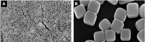
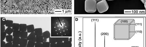
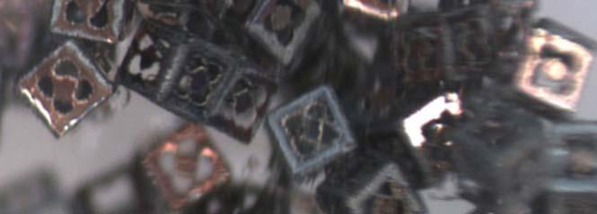
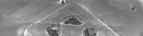
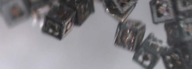
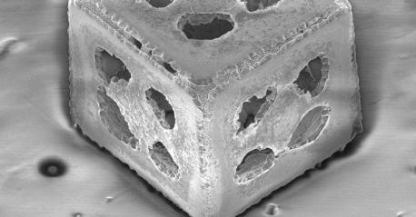
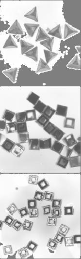
9 Spherical and Shaped Nanoparticles Nanodiamonds Nanocubes Sun & Xia, Science, 2002 Nature, 430, 2004, 190
10 Quantum Dots A quantum dot is a semiconductor nanostructure that confines the motion of conduction band electrons, valence band holes, or excitons (pairs of conduction band electrons and valence band holes) in all three spatial directions. Fluorescence induced by exposure to ultraviolet light in vials containing various sized Cadmium selenide (CdSe) quantum dots From: dots Self-assembly and Nanotechnology

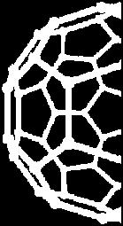
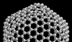
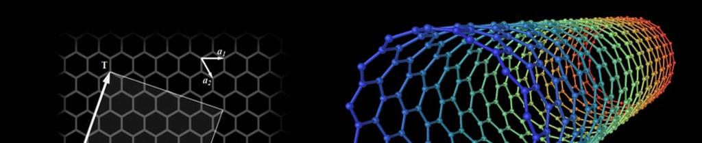
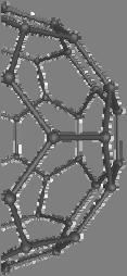
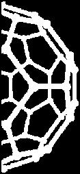
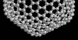
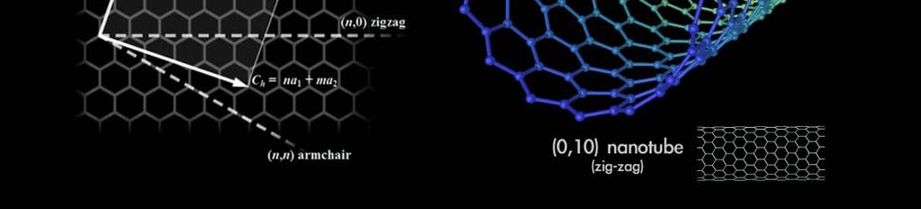
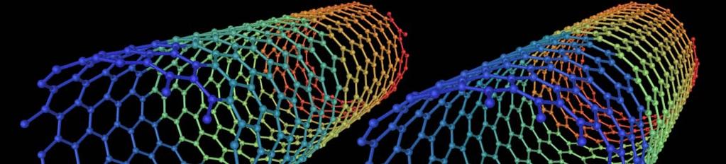
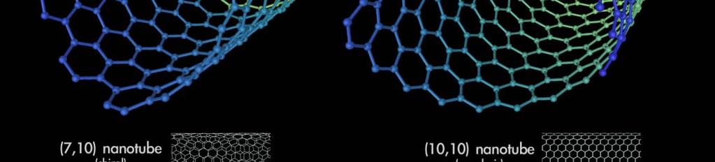
11 Carbon Nanotubes Buckyballs: C60 C540 Carbon nanotubes (CNTs) are an allotrope of carbon (Pictures from Wikipedia) Self-assembly and Nanotechnology
 Diameter 10-20 nm Iijima, S. Carbon nanotubes: past, present, and future.")
12 Single Wall and Multi Wall Carbon Nanotubes Up to cm long SWNT (single Wall nanotube) Diameter ~ 1.4 nm MWNT (multiwall) Diameter nm Iijima, S. Carbon nanotubes: past, present, and future. Physica B: Condensed Matter (2002), 323, 1-5
13 Potential applications of CNs


14 Graphenes Graphene is an atomic-scale honeycomb lattice made of carbon atoms. Optical property The Nobel Prize in Physics 2010 Andre Geim, Konstantin Novoselov
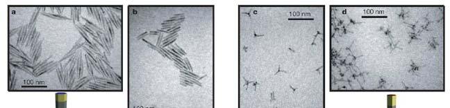
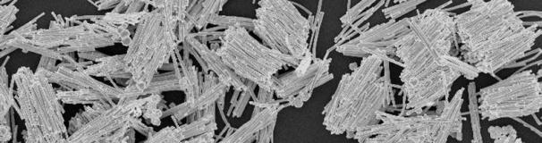
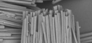
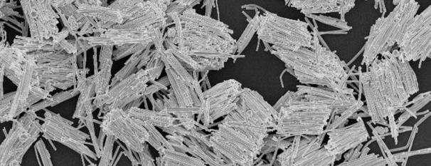
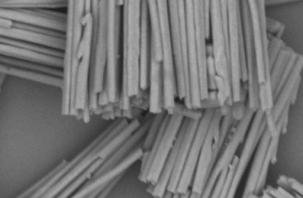
15 Nanowires/Nanorods One component nanowires Multicomponent nanowires Self-assembly and Nanotechnology
16 Optical Properties of Nanoparticles and Nanowires J. Phys. Chem. B, Vol. 109, 2005, Self-assembly and Nanotechnology
17 Molecular Nanostructures Supramolecular nanostructures Self-assembly and Nanotechnology Zeolites (Pictures from Wikipedia)
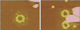
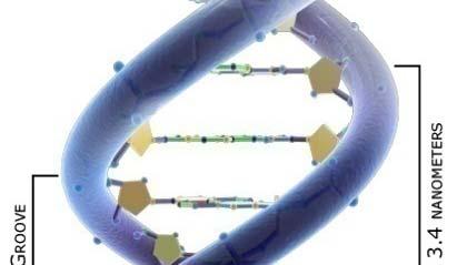
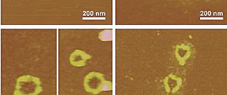
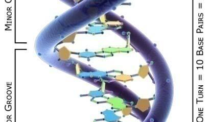
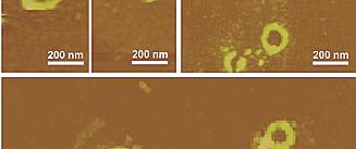

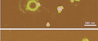
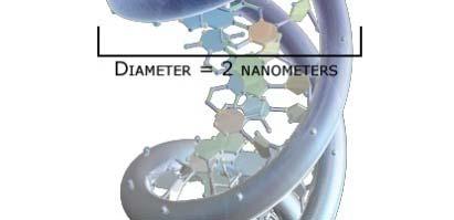
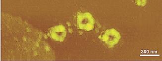
18 Biomolecules: Natural Nanostrucutres DNA (22 to 24 angstroms wide) M13 virus-based ring structures observed by AFM on mica surface Nano Letters, 4 (1), 23-27, 2004
 STM: a")


 The")
19 Scanning Tunneling Microscopy (STM) STM: a new method for confining electrons to artificial structures at the nanometer lengthscale Carbon Monoxide Man Carbon Monoxide on Platinum (111) Iron on Copper (111) The biginning Atom (in Chinese) Xenon on Nickel (110)
20 Dip Pen Nanolithography (DNP)
21 Applications of DPN


22 Nanomotors A nanomotor is a molecular device capable of converting energy into movement and forces on the order of the piconewtons. By attaching a gold plate (with dimensions i of order 100nm) to the outer shell of a suspended multiwall carbon nanotube (like nested carbon cylinders), they are able to electrostatically rotate the outer shell relative to the inner core. These bearings are very robust; Devices have been oscillated thousands of times with no indication of wear. The work was done in situ in an SEM. Nanomotor constructed at UC Berkeley. The motor is about 500nm across: 300 times smaller than the diameter of a human hair
23 Nanocars The nanocar consists of a chassis and axles made of well-defined organic groups with pivoting suspension and freely rotating axles. The wheels are buckyballs. Rice's vehicle is the first that actually functions like a car, rolling on four wheels in a direction perpendicular to its axles. Scanning tunneling microscopy (STM), provided the measurements and experimental evidence that verified the rolling movement

24 Nanotube Field-effect transistor (FET) Transistors are the basic building blocks of integrated circuits (ICs) Applied Physics Letters, vol 73, p (1998)
25 Nanowire-Based Biosensors Materials Today, 2005, 20


 on")

")


26 Nanobiotechnology and Nanomedicine Nanoparticles packed with targeting molecules (red) anchor to integrins (blue) on the outside of a tumor blood vessel cell before shuttling mutant DNA (green) inside Molecular switchs that can turn on and off enzyme Patterned carbon nanofibers control chemical release to cells


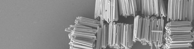
27 Nanowire Lasers and Photonics Nanowire lasers (Nature, Vol 421, 2003, 241) Nanowires for Integrated Multicolor Nanophotonics (Small, 2005, 1, 142)


28 Nanowire Dye-Sensitized Solar Cells The nanowire dye-sensitized cell, based on a ZnO wire array Nature Materials vol 4, 2005, 455
29 More and more applications in Nano-xxxxxx

30 Break! Nano-Break!!!
31 Section II: Self-assembly
32 What s self-assembly??? Self-assembly is the fundamental principle which generates structural organization on all scales from molecules to galaxies. It is defined as reversible processes in which pre-existing parts or disordered d d components of a preexisting system form structures t of patterns. Examples of self-assembling system include weather patterns, solar systems, histogenesis (formation of different tissues from undifferentiated cells ) and self-assembled monolayers. The most wellstudied subfield of self-assembly is molecular self-assembly From Wikipedia: Self-assembly and Nanotechnology
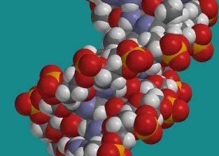
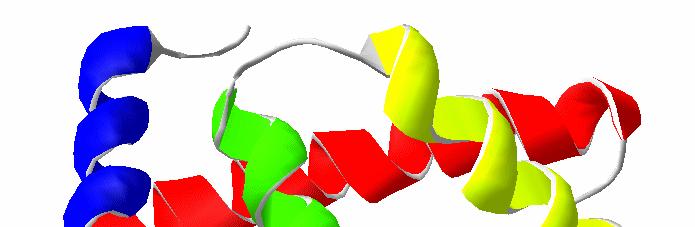
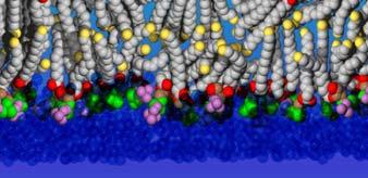
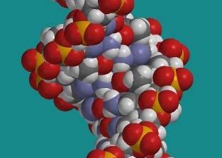
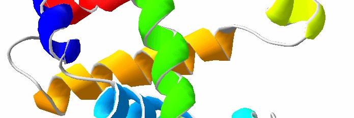
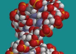

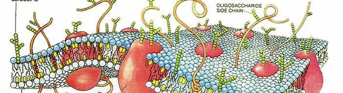
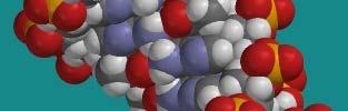
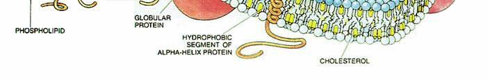
33 Self-Assembly in Living Systems Lipid bilayer DNA double-helix Protein: A representation of the 3D structure of myoglobin Protein folding Cell Membrane
34 Self-assembled Monolayers (SAMs) Surface modification Corrosion inhibition Biocompatibility Self-assembly and Nanotechnology

 Amphiphilic")
35 Self-Assembly of Molecules Surfactant micelles Complex block copolymer structures Sodium dodecylsulfate (SDS) Amphiphilic block copolymers


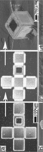
36 Self-Assembly of Electronic Systems Millimeter scale Gracias, Tien, Breen, Hsu, Whitesides. Science 2000, 289, μm scale Jacobs, Tao, Schwartz, Gracias, Whitesides. Science 2002, 296, 323. Self-assembly and Nanotechnology


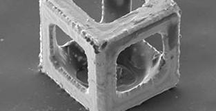
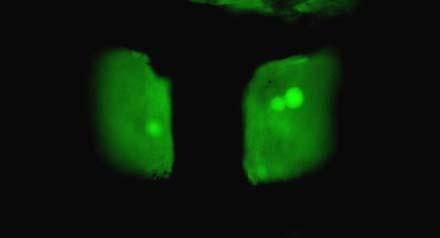
37 Self-Assembled Micro-Containers μm Gimi, Leong, Gu, Yang, Artemov, Bhujwalla, Gracias. Biomedical Microdevices 2005, 7, Self-assembly and Nanotechnology
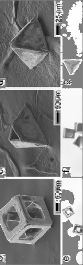
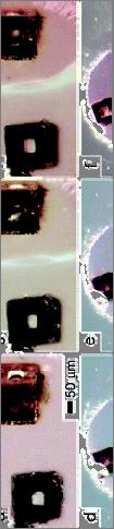
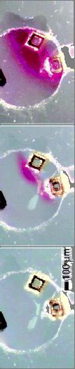
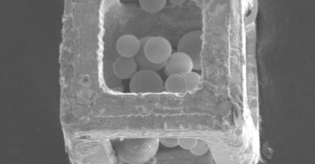
38 Self-Assembled Micro-Containers Leong, Gu, Koh, Gracias. JACS 2006, 128,


39 Self-Assembly of Nanowires Magnetic assembly Park, Lim, Chung, Mirkin. Science 2004, 303, 348 Love, Urbach, Prentiss, Whitesides. JACS, 2003, 125,
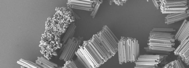
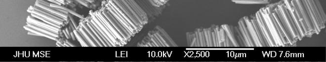
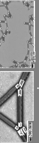
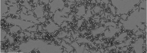
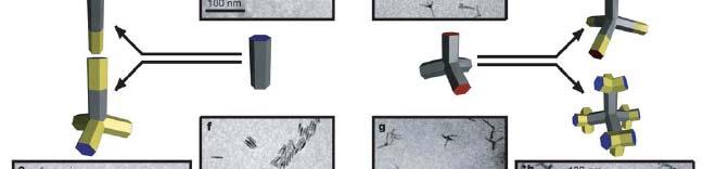
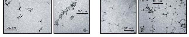
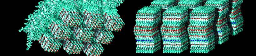
40 Self-Assembly of Nanowires Glued 3D bundles Large scale bundles during membrane dissolution Glued 2D networks Self-assembly and Nanotechnology Gu, Chen, Gracias. Langmuir 2004, 20,11308.
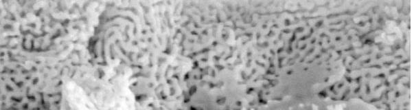
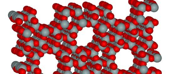
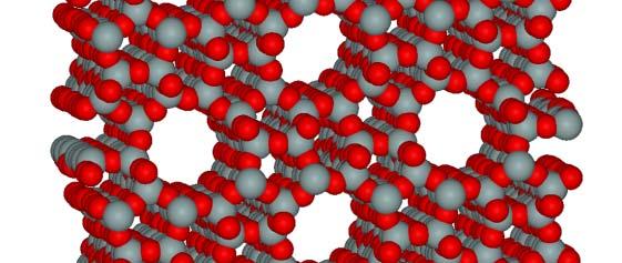
41 Self-assembly: Nanoporous Gold Erlebacher, Aziz, Karma, Dimitrov, Sieradzki. Nature 2001, 410, Self-assembly and Nanotechnology
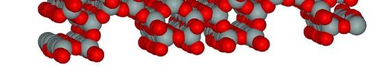
42 Self-assembly: Nanoporous AAO membranes Whatman Separation Nanowire, nanotube fabrication Biomedical engineering i nm pore size Self-assembly and Nanotechnology


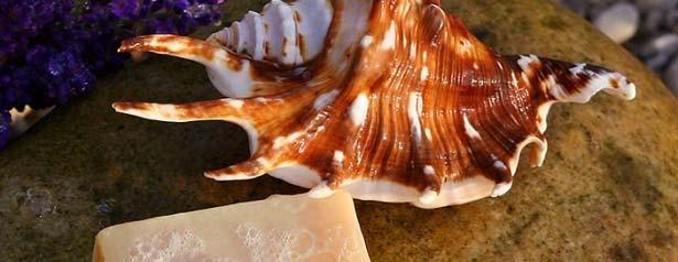
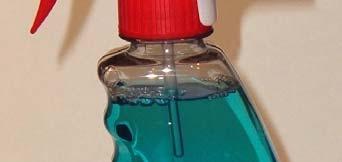
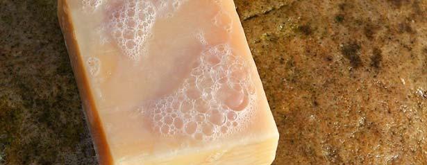

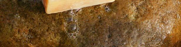

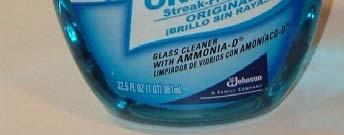
43 Personal and Home Products Soap Detergent Self-assembly and Nanotechnology


44 Pharmaceutical and Health Products For creams and lotions Emulsions 20 ml ampule of 1% propofol emulsion suitable for intravenous injection. The manufacturers emulsify the lipid soluble propofol in a mixture of water, soy oil and egg lecitin. Self-assembly and Nanotechnology
45 Self-assembly: Molecular Electronics Nanowires are assembled into crossbars (left). Organic molecules between crossing wires serve as transistors (right) Self-assembly and Nanotechnology
46 Self-assembly: New Structures and New Materials Hierarchically ordered oxide through a combination of microchannel, microsphere, and block-copolymer templating Ozin and Arsenault. Nanochemistry: A Chemical Approach to Nanomaterials. RSC Publishing, 2005
47 Self-assembling route to Nanotechnology A flowchart delineating the factors that must be considered when approaching the self-assembly of a nanoscale system Ozin and Arsenault. Nanochemistry: A Chemical Approach to Nanomaterials. RSC Publishing, 2005
48 Self-assembly and Nanotechnology New materials, new technologies Self-assembly Nanotechnology New applications, new products Self-assembly and Nanotechnology


49 Perspectives, Potentials and Challenges Trillions of dollars business in the next ten years or so Energy Information storage Does everything have to be nano?? Is nano good or not? Nanotoxicity Environment, health and safety Self-assembly and Nanotechnology
50 Course Project Literature search methods; 1-page Abstract/Outline, due on Feb. 6 (third week), preferred by Literature review due, Feb. 27 Project update presentation and discussion, Progress report (I) due, March 27. Final presentations, May 1 Final Report Due on exam day, sent by Self-assembly and Nanotechnology
29: Nanotechnology. What is Nanotechnology? Properties Control and Understanding. Nanomaterials
 29: Nanotechnology What is Nanotechnology? Properties Control and Understanding Nanomaterials Making nanomaterials Seeing at the nanoscale Quantum Dots Carbon Nanotubes Biology at the Nanoscale Some Applications
Nanotechnology. Yung Liou P601 Institute of Physics Academia Sinica
 Nanotechnology Yung Liou P601 yung@phys.sinica.edu.tw Institute of Physics Academia Sinica 1 1st week Definition of Nanotechnology The Interagency Subcommittee on Nanoscale Science, Engineering and Technology
RAJASTHAN TECHNICAL UNIVERSITY, KOTA
 RAJASTHAN TECHNICAL UNIVERSITY, KOTA (Electronics & Communication) Submitted By: LAKSHIKA SOMANI E&C II yr, IV sem. Session: 2007-08 Department of Electronics & Communication Geetanjali Institute of Technical
Nanotechnology? Source: National Science Foundation (NSF), USA
, USA") 2 2 Nanotechnology? Ability to work at the atomic, molecular and even sub-molecular levels in order to create and use material structures, devices and systems with new properties and functions Source:
2 2 Nanotechnology? Ability to work at the atomic, molecular and even sub-molecular levels in order to create and use material structures, devices and systems with new properties and functions Source:
In the name of Allah
 In the name of Allah Nano chemistry- 4 th stage Lecture No. 1 History of nanotechnology 16-10-2016 Assistance prof. Dr. Luma Majeed Ahmed lumamajeed2013@gmail.com, luma.ahmed@uokerbala.edu.iq Nano chemistry-4
PHYS 3313 Section 001 Lecture #21 Monday, Nov. 26, 2012
 PHYS 3313 Section 001 Lecture #21 Monday, Nov. 26, 2012 Superconductivity Theory, The Cooper Pair Application of Superconductivity Semi-Conductor Nano-technology Graphene 1 Announcements Your presentations
Nanotechnology Fabrication Methods.
 Nanotechnology Fabrication Methods. 10 / 05 / 2016 1 Summary: 1.Introduction to Nanotechnology:...3 2.Nanotechnology Fabrication Methods:...5 2.1.Top-down Methods:...7 2.2.Bottom-up Methods:...16 3.Conclusions:...19
Home News Nano Databases Nano Business Nano Jobs Resources Introduction to Nanotechnology
 1 of 7 7/18/2013 2:54 PM Open menu Home News Nano Databases Nano Business Nano Jobs Resources Introduction to Nanotechnology The latest news from academia, regulators research labs and other things of
Nanotechnology. Gavin Lawes Department of Physics and Astronomy
 Nanotechnology Gavin Lawes Department of Physics and Astronomy Earth-Moon distance 4x10 8 m (courtesy NASA) Length scales (Part I) Person 2m Magnetic nanoparticle 5x10⁻⁹ m 10 10 m 10 5 m 1 m 10-5 m 10-10
Nanostructures. Lecture 13 OUTLINE
 Nanostructures MTX9100 Nanomaterials Lecture 13 OUTLINE -What is quantum confinement? - How can zero-dimensional materials be used? -What are one dimensional structures? -Why does graphene attract so much
Nanomaterials and their Optical Applications
 Nanomaterials and their Optical Applications Winter Semester 2013 Lecture 02 rachel.grange@uni-jena.de http://www.iap.uni-jena.de/multiphoton Lecture 2: outline 2 Introduction to Nanophotonics Theoretical
Nanotechnology where size matters
 Nanotechnology where size matters J Emyr Macdonald Overview Ways of seeing very small things What is nanotechnology and why is it important? Building nanostructures What we can do with nanotechnology?
Final Reading Assignment: Travels to the Nanoworld: pages pages pages
 Final Reading Assignment: Travels to the Nanoworld: pages 152-164 pages 201-214 pages 219-227 Bottom-up nanofabrication Can we assemble nanomachines manually? What are the components (parts)? nanoparticles
Like space travel and the Internet before it, the possibilities of the nano world catches the imagination of school children and scientists alike.
 The Nano World Preface Nano is the cool thing and it s the buzzword Like space travel and the Internet before it, the possibilities of the nano world catches the imagination of school children and scientists
CHAPTER 11 Semiconductor Theory and Devices
 CHAPTER 11 Semiconductor Theory and Devices 11.1 Band Theory of Solids 11.2 Semiconductor Theory 11.3 Semiconductor Devices 11.4 Nanotechnology It is evident that many years of research by a great many
SPECIFIC USES OR APPLICATIONS OF NANOSTRUCTURES; MEASUREMENT OR ANALYSIS OF NANOSTRUCTURES; MANUFACTURE OR TREATMENT OF NANOSTRUCTURES
 CPC - B82Y - 2017.08 B82Y SPECIFIC USES OR APPLICATIONS OF NANOSTRUCTURES; MEASUREMENT OR ANALYSIS OF NANOSTRUCTURES; MANUFACTURE OR TREATMENT OF NANOSTRUCTURES Definition statement This place covers:
NANOMEDICINE. WILEY A John Wiley and Sons, Ltd., Publication DESIGN AND APPLICATIONS OF MAGNETIC NANOMATERIALS, NANOSENSORS AND NANOSYSTEMS
 NANOMEDICINE DESIGN AND APPLICATIONS OF MAGNETIC NANOMATERIALS, NANOSENSORS AND NANOSYSTEMS Vijay K. Varadan Linfeng Chen Jining Xie WILEY A John Wiley and Sons, Ltd., Publication Preface About the Authors
PV Tutorial Allen Hermann, Ph. D. Professor of Physics Emeritus, and Professor of Music Adjunct, University of Colorado, Boulder, Colorado, USA and
 PV Tutorial Allen Hermann, Ph. D. Professor of Physics Emeritus, and Professor of Music Adjunct, University of Colorado, Boulder, Colorado, USA and Vice-president, NanoTech Inc. Lexington, Kentucky, USA
In today s lecture, we will cover:
 In today s lecture, we will cover: Metal and Metal oxide Nanoparticles Semiconductor Nanocrystals Carbon Nanotubes 1 Week 2: Nanoparticles Goals for this section Develop an understanding of the physical
Seminars in Nanosystems - I
 Seminars in Nanosystems - I Winter Semester 2011/2012 Dr. Emanuela Margapoti Emanuela.Margapoti@wsi.tum.de Dr. Gregor Koblmüller Gregor.Koblmueller@wsi.tum.de Seminar Room at ZNN 1 floor Topics of the
NANOSCIENCE AND NANOTECHNOLOGY
 NANOSCIENCE AND NANOTECHNOLOGY Yuehe Lin WHAT IS NANOTECHNOLOGY Nanotechnology is the understanding and control of matter at dimensions of roughly 1 to 100 nanometers, where unique phenomena enable novel
PHYS 3313 Section 001 Lecture #24 Monday, Apr. 21, 2014
 PHYS 3313 Section 001 Lecture #24 Monday, Apr. 21, 2014 Liquid Helium Superconductivity Theory, The Cooper Pair Application of Superconductivity Nano-technology Graphene 1 Announcements Reminder Homework
672 Advanced Solid State Physics. Scanning Tunneling Microscopy
 672 Advanced Solid State Physics Scanning Tunneling Microscopy Biao Hu Outline: 1. Introduction to STM 2. STM principle & working modes 3. STM application & extension 4. STM in our group 1. Introduction
CHEM 6342 Nanotechnology Fundamentals and Applications. Dieter Cremer, 325 FOSC, ext ,
 D. Cremer, CHEM 6342, Nanotechnology - Fundamentals and Applications 1 CHEM 6342 Nanotechnology Fundamentals and Applications Class location: Lectures, time and location: Lab times and location: Instructor:
Introduction to Nanoscience and Nanotechnology
 Introduction to Nanoscience and Nanotechnology ENS 463 by Alexander M. Zaitsev alexander.zaitsev@csi.cuny.edu Tel: 718 982 2812 Office 4N101b 1 What is the size for a nano? 10-3 m, (milli) Macroobjects,
Nanobiotechnology. Place: IOP 1 st Meeting Room Time: 9:30-12:00. Reference: Review Papers. Grade: 40% midterm, 60% final report (oral + written)
") Nanobiotechnology Place: IOP 1 st Meeting Room Time: 9:30-12:00 Reference: Review Papers Grade: 40% midterm, 60% final report (oral + written) Midterm: 5/18 Oral Presentation 1. 20 minutes each person
Nanobiotechnology Place: IOP 1 st Meeting Room Time: 9:30-12:00 Reference: Review Papers Grade: 40% midterm, 60% final report (oral + written) Midterm: 5/18 Oral Presentation 1. 20 minutes each person
not to be confused with using the materials to template nanostructures
 Zeolites as Templates: continued Synthesis: Most zeolite syntheses are performed by using template-synthesis not to be confused with using the materials to template nanostructures templates are often surfactants
LECTURE 1 : INTRODUCTION TO NANOMECHANICS
 I LECTURE 1 : INTRODUCTION TO NANOMECHANICS Outline : NANOTECHNOLOGY / NANOMECHANICS DEFINITIONS... 2 WHY IS NANO INTERESTING?... 3 HISTORY OF NANOTECHNOLOGY/NANOMECHANICS : TIME LINE... 4 The First Talk
Nanoparticles, nanorods, nanowires
 Nanoparticles, nanorods, nanowires Nanoparticles, nanocrystals, nanospheres, quantum dots, etc. Drugs, proteins, etc. Nanorods, nanowires. Optical and electronic properties. Organization using biomolecules.
Understanding the properties and behavior of groups of interacting atoms more than simple molecules
 Condensed Matter Physics Scratching the Surface Understanding the properties and behavior of groups of interacting atoms more than simple molecules Solids and fluids in ordinary and exotic states low energy
There's Plenty of Room at the Bottom
 There's Plenty of Room at the Bottom 12/29/1959 Feynman asked why not put the entire Encyclopedia Britannica (24 volumes) on a pin head (requires atomic scale recording). He proposed to use electron microscope
NANOTECHNOLOGY. Students will gain an understanding of nanoscale dimensions and nanotechnology.
 NANOTECHNOLOGY By Anna M. Waldron and Carl A. Batt, Nanobiotechnology Center, Cornell University Subjects: Nanotechnology, Chemistry, Physics Time: Two class periods (approximately 90 minutes) Objective:
Subject Index. See https://pubs.acs.org/sharingguidelines for options on how to legitimately share published articles.
 Subject Index Downloaded via 148.251.232.83 on July 22, 2018 at 01:11:58 (UTC). See https://pubs.acs.org/sharingguidelines for options on how to legitimately share published articles. A American Chemical
Chapter 1 Introduction
 Chapter 1 Introduction A nanometer (nm) is one billionth (10-9 ) of a meter. Nanoscience can be defined as the science of objects and phenomena occurring at the scale of 1 to 100 nm. The range of 1 100
1.1. Introduction to Nanoscience and Nanotechnology
 1.1. Introduction to Nanoscience and Nanotechnology 1.1.1. A Brief Historical Overview Before trying to understand and discuss about synthesis, characterization and application of nanomaterials, it is
Lesson 4: Tools of the Nanosciences. Student Materials
 Lesson 4: Tools of the Nanosciences Student Materials Contents Black Box Lab Activity: Student Instructions and Worksheet Seeing and Building Small Things: Student Reading Seeing and Building Small Things:
SELF-ASSEMBLY AND NANOTECHNOLOGY A Force Balance Approach
 SELF-ASSEMBLY AND NANOTECHNOLOGY A Force Balance Approach Yoon S. Lee Scientific Information Analyst Chemical Abstracts Service A Division of the American Chemical Society Columbus, Ohio WILEY A JOHN WILEY
Electrochemically Synthesized Multi-block
 Electrochemically Synthesized Multi-block Nanorods Sungho Park SungKyunKwan University, Department of Chemistry & SKKU Advanced Institute of Nanotechnology (SAINT) J. Am. Chem. Soc. 2003, 125, 2282-2290
Lecture 2. Methods and Techniques for Self-assembly
 10.524 Lecture 2. Methods and Techniques for Self-assembly Instructor: Prof. Zhiyong Gu (Chemical Engineering & UML CHN/NCOE Nanomanufacturing Center) Lecture 2: Methods and Techniques for Self-assembly
master thesis STM studies of molecules for molecular electronics
 STM studies of molecules for molecular electronics Experimental study of single organic molecules by Scanning Tunneling Microscope (STM) and spectroscopy at low temperature Experimental STM images of Aza-BODIPY
Nanotubes and Nanowires - One-dimensional Materials
 NCLT July 13th, 2006 Nanotubes and Nanowires - One-dimensional Materials Tim Sands Materials Engineering and Electrical & Computer Engineering Birck Nanotechnology Center Purdue University 100 nm Si/SiGe
26.542: COLLOIDAL NANOSCIENCE & NANOSCALE ENGINEERING Fall 2013
 26.542: COLLOIDAL NANOSCIENCE & NANOSCALE ENGINEERING Fall 2013 Classes: Thurs, 6-9 pm; Ball Hall Room 208 Professor: Dr. B. Budhlall Office: Ball Hall 203B, Phone: 978-934-3414 Email: Bridgette_Budhlall@uml.edu
Carbon Nanomaterials: Nanotubes and Nanobuds and Graphene towards new products 2030
 Carbon Nanomaterials: Nanotubes and Nanobuds and Graphene towards new products 2030 Prof. Dr. Esko I. Kauppinen Helsinki University of Technology (TKK) Espoo, Finland Forecast Seminar February 13, 2009
CH676 Physical Chemistry: Principles and Applications. CH676 Physical Chemistry: Principles and Applications
 CH676 Physical Chemistry: Principles and Applications History of Nanotechnology: Time Line Democritus in ancient Greece: concept of atom 1900 : Rutherford : discovery of atomic nucleus The first TEM was
SYLLABUS FINDING NANO Syllabus NanoSCI DISCOVERING NANOTECHNOLOGY AND CULTURE IN GERMANY
 1. Syllabus NanoSCI Course title: NanoSCI - Electronic Properties of Nanoengineered Materials Catalog description: Physics and technology of nanoengineered materials and devices. Semiconductor nanostructures.
Lecture 2. Fundamentals and Theories of Self-Assembly
 10.524 Lecture 2. Fundamentals and Theories of Self-Assembly Instructor: Prof. Zhiyong Gu (Chemical Engineering & UML CHN/NCOE Nanomanufacturing Center) Lecture 2: Fundamentals and Theories of Self-Assembly
Electrical and Optical Properties. H.Hofmann
 Introduction to Nanomaterials Electrical and Optical Properties H.Hofmann Electrical Properties Ohm: G= σw/l where is the length of the conductor, measured in meters [m], A is the cross-section area of
There s plenty of room at the bottom! - R.P. Feynman, Nanostructure: a piece of material with at least one dimension less than 100 nm in extent.
 Nanostructures and Nanotechnology There s plenty of room at the bottom! - R.P. Feynman, 1959 Materials behave differently when structured at the nm scale than they do in bulk. Technologies now exist that
EN2912C: Future Directions in Computing Lecture 08: Overview of Near-Term Emerging Computing Technologies
 EN2912C: Future Directions in Computing Lecture 08: Overview of Near-Term Emerging Computing Technologies Prof. Sherief Reda Division of Engineering Brown University Fall 2008 1 Near-term emerging computing
3-month progress Report
 3-month progress Report Graphene Devices and Circuits Supervisor Dr. P.A Childs Table of Content Abstract... 1 1. Introduction... 1 1.1 Graphene gold rush... 1 1.2 Properties of graphene... 3 1.3 Semiconductor
1. Nanotechnology & nanomaterials -- Functional nanomaterials enabled by nanotechnologies.
 Novel Nano-Engineered Semiconductors for Possible Photon Sources and Detectors NAI-CHANG YEH Department of Physics, California Institute of Technology 1. Nanotechnology & nanomaterials -- Functional nanomaterials
Course file PPY15204 Nanoscience and Nanomaterials Table of Contents
 Department Physics Nanotechnology : M.sc Physics Course file PPY15204 Table Contents Second Year MSc Physics (2015-2016 Regulation) Detailed Lesson Plan UNIT-I: INTRODUCTION TO NANOTECHNOLOGY History Importance
Special Topics in Semiconductor Nanotechnology ECE 598XL
 Special Topics in Semiconductor Nanotechnology ECE 598XL Fall 2009 ECE 598XL Syllabus Overview: size matters Formation Process Characterization SOA device applications and potentials Homework or quizzes
Carbon Nanomaterials
 Carbon Nanomaterials STM Image 7 nm AFM Image Fullerenes C 60 was established by mass spectrographic analysis by Kroto and Smalley in 1985 C 60 is called a buckminsterfullerene or buckyball due to resemblance
Nanostrukturphysik (Nanostructure Physics)
") Nanostrukturphysik (Nanostructure Physics) Prof. Yong Lei & Dr. Huaping Zhao Fachgebiet Angewandte Nanophysik, Institut für Physik Contact: yong.lei@tu-ilmenau.de; huaping.zhao@tu-ilmenau.de Office: Unterpoerlitzer
Nanostrukturphysik (Nanostructure Physics) Prof. Yong Lei & Dr. Huaping Zhao Fachgebiet Angewandte Nanophysik, Institut für Physik Contact: yong.lei@tu-ilmenau.de; huaping.zhao@tu-ilmenau.de Office: Unterpoerlitzer
Nanotechnology Nanofabrication of Functional Materials. Marin Alexe Max Planck Institute of Microstructure Physics, Halle - Germany
 Nanotechnology Nanofabrication of Functional Materials Marin Alexe Max Planck Institute of Microstructure Physics, Halle - Germany Contents Part I History and background to nanotechnology Nanoworld Nanoelectronics
2 Symmetry. 2.1 Structure of carbon nanotubes
 2 Symmetry Carbon nanotubes are hollow cylinders of graphite sheets. They can be viewed as single molecules, regarding their small size ( nm in diameter and µm length), or as quasi-one dimensional crystals
CH676 Physical Chemistry: Principles and Applications. CH676 Physical Chemistry: Principles and Applications
 CH676 Physical Chemistry: Principles and Applications Contact Information Professor Chia-Kuang (Frank) Tsung Email: frank.tsung@bc.edu Office: Merkert 224; Phone: (617) 552-8927 Office Hours: Monday 5-6
Figure 1: Some examples of objects at different size scales ( 2001, CMP Científica, [2])
![Figure 1: Some examples of objects at different size scales ( 2001, CMP Científica, [2])](/thumbs/85/91872790.jpg "Figure 1: Some examples of objects at different size scales ( 2001, CMP Científica, [2])") Top-Down vs. Bottom-Up Nanomanufacturing Prof. Derek J. Hansford, Biomedical Engineering Program and Department of Materials Science & Engineering Learning Objectives: This module should expose the student
Top-Down vs. Bottom-Up Nanomanufacturing Prof. Derek J. Hansford, Biomedical Engineering Program and Department of Materials Science & Engineering Learning Objectives: This module should expose the student
What is the role of simulation in nanoscience research?
 ChE/MSE 557 Intro part 2 What is the role of simulation in nanoscience research? 1 Opportunities for Simulation Simulation Simulation complements both experiment and theory. Extends window of observation
NANOSCIENCE: TECHNOLOGY AND ADVANCED MATERIALS
 UNIVERSITY OF SOUTHAMPTON PHYS6014W1 SEMESTER 2 EXAMINATIONS 2012-2013 NANOSCIENCE: TECHNOLOGY AND ADVANCED MATERIALS DURATION 120 MINS (2 Hours) This paper contains 8 questions Answer ALL questions in
Materials. Definitions of nanotechnology. The term nanotechnology was invented by Professor Norio Taniguchi at the University of Tokyo in 1971.
 Materials Definitions of nanotechnology The term nanotechnology was invented by Professor Norio Taniguchi at the University of Tokyo in 1971. The original definition, translated into English Nano-technology'
Lectures Graphene and
 Lectures 15-16 Graphene and carbon nanotubes Graphene is atomically thin crystal of carbon which is stronger than steel but flexible, is transparent for light, and conducts electricity (gapless semiconductor).
Nanotechnology 5 th lecture
 Nanotechnology 5 th lecture (c) http://www.nccr-nano.org/nccr_data/ gallery/gallery_01/gallery_01_03/pics_06/ internet/nanotube_spiral.jpg Plan for today: http://www.nccr-nano.org/nccr_data/gallery/ gallery_01/gallery_01_03/pics_04/internet/
CSCI 2570 Introduction to Nanocomputing
 CSCI 2570 Introduction to Nanocomputing The Emergence of Nanotechnology John E Savage Purpose of the Course The end of Moore s Law is in sight. Researchers are now exploring replacements for standard methods
Physics and Material Science of Semiconductor Nanostructures
 Physics and Material Science of Semiconductor Nanostructures PHYS 570P Prof. Oana Malis Email: omalis@purdue.edu Course website: http://www.physics.purdue.edu/academic_programs/courses/phys570p/ 1 Course
NANOTECHNOLOGY SOLID WASTE IMPLICATIONS. Gurumurthy Ramachandran. University of Minnesota
 NANOTECHNOLOGY SOLID WASTE IMPLICATIONS Gurumurthy Ramachandran University of Minnesota Engineering at the Atomic Level: Scanning Tunneling Microscopy Manipulating atoms Writing with atoms. D.M. Eigler,
Nanostrukturphysik (Nanostructure Physics)
") Nanostrukturphysik (Nanostructure Physics) Prof. Yong Lei & Dr. Yang Xu Fachgebiet 3D-Nanostrukturierung, Institut für Physik Contact: yong.lei@tu-ilmenau.de; yang.xu@tu-ilmenau.de Office: Unterpoerlitzer
Nanostrukturphysik (Nanostructure Physics) Prof. Yong Lei & Dr. Yang Xu Fachgebiet 3D-Nanostrukturierung, Institut für Physik Contact: yong.lei@tu-ilmenau.de; yang.xu@tu-ilmenau.de Office: Unterpoerlitzer
Welcome to NANO* 2000
 Lecture Zero Welcome to NANO* 2000 First - the "big picture" of the course and the course outline -grading scheme - exam schedule - review paper - lab (Jay) last revision September 4 2013: MDB 0-1 NANO*
ME 4875/MTE C/18. Introduction to Nanomaterials and Nanotechnology. Lecture 1 - Introduction
 ME 4875/MTE 575 - C/18 Introduction to Nanomaterials and Nanotechnology Lecture 1 - Introduction 1 Course Information Syllabus uploaded to Canvas Schedule: Lectures MT-RF 10:00-10:50 pm in Olin Hall 223
Quantized Electrical Conductance of Carbon nanotubes(cnts)
") Quantized Electrical Conductance of Carbon nanotubes(cnts) By Boxiao Chen PH 464: Applied Optics Instructor: Andres L arosa Abstract One of the main factors that impacts the efficiency of solar cells is
Quantized Electrical Conductance of Carbon nanotubes(cnts) By Boxiao Chen PH 464: Applied Optics Instructor: Andres L arosa Abstract One of the main factors that impacts the efficiency of solar cells is
LAYER BY LAYER (LbL) SELF-ASSEMBLY STRATEGY AND ITS APPLICATIONS
 SELF-ASSEMBLY STRATEGY AND ITS APPLICATIONS") LAYER BY LAYER (LbL) SELF-ASSEMBLY STRATEGY AND ITS APPLICATIONS A. Z. Cheng 1, R. Swaminathan 2 1 Nanotechnology Engineering, University of Waterloo, azcheng@uwaterloo.ca; 2 Nanotechnology Engineering,
LAYER BY LAYER (LbL) SELF-ASSEMBLY STRATEGY AND ITS APPLICATIONS A. Z. Cheng 1, R. Swaminathan 2 1 Nanotechnology Engineering, University of Waterloo, azcheng@uwaterloo.ca; 2 Nanotechnology Engineering,
Scripts for High School Visits to the Herman Group at Columbia University
 Scripts for High School Visits to the Herman Group at Columbia University Evan Spotte-Smith, Jiayang Hu, and Irving P. Herman April, 2017; updated June, 2017 These presentations were developed for visits
Inorganic compounds that semiconduct tend to have an average of 4 valence electrons, and their conductivity may be increased by doping.
 Chapter 12 Modern Materials 12.1 Semiconductors Inorganic compounds that semiconduct tend to have an average of 4 valence electrons, and their conductivity may be increased by doping. Doping yields different
Summerschool 2014 Nanophysics
 Summerschool 2014 Nanophysics For numerical applications one may (crudely) assume the following values: Reduced Planck constant hbar=h/2π=10-34 S.I. Electron charge e=10-19 C Boltzmann constant k B =10-23
ME 4875/MTE C/16. Introduction to Nanomaterials and Nanotechnology. Lecture 1 - Introduction
 ME 4875/MTE 575 - C/16 Introduction to Nanomaterials and Nanotechnology Lecture 1 - Introduction 1 Course Information Syllabus uploaded to mywpi Schedule: Lectures MT-RF 2:00-2:50 pm in Salisbury Labs
Fabrication Methods: Chapter 4. Often two methods are typical. Top Down Bottom up. Begins with atoms or molecules. Begins with bulk materials
 Fabrication Methods: Chapter 4 Often two methods are typical Top Down Bottom up Begins with bulk materials Begins with atoms or molecules Reduced in size to nano By thermal, physical Chemical, electrochemical
Jeopardy Q $100 Q $100 Q $100 Q $100 Q $100 Q $200 Q $200 Q $200 Q $200 Q $200 Q $300 Q $300 Q $300 Q $300 Q $300 Q $400 Q $400 Q $400 Q $400 Q $400
 Jeopardy Size and Scale Nano Products Tools Structure Of Matter Science and Society Q $100 Q $200 Q $300 Q $400 Q $500 Q $100 Q $100 Q $100 Q $100 Q $200 Q $200 Q $200 Q $200 Q $300 Q $300 Q $300 Q $300
Graphene The Search For Two Dimensions. Christopher Scott Friedline Arizona State University
 Graphene The Search For Two Dimensions Christopher Scott Friedline Arizona State University What Is Graphene? Single atomic layer of graphite arranged in a honeycomb crystal lattice Consists of sp 2 -bonded
Surface Plasmon Resonance in Metallic Nanoparticles and Nanostructures
 Surface Plasmon Resonance in Metallic Nanoparticles and Nanostructures Zhi-Yuan Li Optical Physics Laboratory, Institute of Physics, CAS Beijing 18, China January 5-9, 7, Fudan University, Shanghai Challenges
Dip-Pen Lithography 1
 Dip-Pen Lithography 1 A Brief History of Writing Instruments From Quills and Bamboos to fountain pens and brushes M. Klein and Henry W. Wynne received US patent #68445 in 1867 for an ink chamber and delivery
Carbon Nanotubes: The Hub Of Nanoelectronics
 Carbon Nanotubes: The Hub Of Nanoelectronics P.I. Okwu 1 and I.N. Onyeje 2 1 Deputy Director, Electronics Development Institute (ELDI) Awka, Nigeria 2 Department of Electrical/Electronic Engineering, Anambra
Supporting Information for
 Supporting Information for Multilayer CuO@NiO Hollow Spheres: Microwave-Assisted Metal-Organic-Framework Derivation and Highly Reversible Structure-Matched Stepwise Lithium Storage Wenxiang Guo, Weiwei
Novel Nanoparticles for Ultrasensitive Detection and Spectroscopy
 Final Technical Report (DOE-FG02-98ER14873) Project Officer: Dr. Richard Gordon / Dr. John Miller Novel Nanoparticles for Ultrasensitive Detection and Spectroscopy Shuming Nie Indiana University P. 0.
Nanostrukturphysik (Nanostructure Physics)
") Nanostrukturphysik (Nanostructure Physics) Prof. Yong Lei & Dr. Yang Xu Fachgebiet 3D-Nanostrukturierung, Institut für Physik Contact: yong.lei@tu-ilmenau.de; yang.xu@tu-ilmenau.de Office: Unterpoerlitzer
Nanostrukturphysik (Nanostructure Physics) Prof. Yong Lei & Dr. Yang Xu Fachgebiet 3D-Nanostrukturierung, Institut für Physik Contact: yong.lei@tu-ilmenau.de; yang.xu@tu-ilmenau.de Office: Unterpoerlitzer
Techniken der Oberflächenphysik (Technique of Surface Physics)
") Techniken der Oberflächenphysik (Technique of Surface Physics) Yong Lei & Fabian Grote Fachgebiet 3D-Nanostrukturierung, Institut für Physik Contact: yong.lei@tu-ilmenau.de; fabian.grote@tu-ilmenau.de
Techniken der Oberflächenphysik (Technique of Surface Physics) Yong Lei & Fabian Grote Fachgebiet 3D-Nanostrukturierung, Institut für Physik Contact: yong.lei@tu-ilmenau.de; fabian.grote@tu-ilmenau.de
Unconventional Nano-patterning. Peilin Chen
 Unconventional Nano-patterning Peilin Chen Reference Outlines History of patterning Traditional Nano-patterning Unconventional Nano-patterning Ancient Patterning "This is the Elks' land". A greeting at
FACULTY OF ENGINEERING ALEXANDRIA UNVERSITY. Solid State lab. Instructors Dr. M. Ismail El-Banna Dr. Mohamed A. El-Shimy TA Noha Hanafy
 FACULTY OF ENGINEERING ALEXANDRIA UNVERSITY Solid State lab Instructors Dr. M. Ismail El-Banna Dr. Mohamed A. El-Shimy TA Noha Hanafy 2017-2018 first term A. Experiments 1- Relationship between the intensity
Investigating Nano-Space
 Name Partners Date Visual Quantum Mechanics The Next Generation Investigating Nano-Space Goal You will apply your knowledge of tunneling to understand the operation of the scanning tunneling microscope.
Lesson 1: Introduction to Nanoscience. Teacher Materials
 Lesson 1: Introduction to Nanoscience Teacher Materials Contents Introduction to Nanoscience: Teacher Lesson Plan Introduction to Nanoscience: PowerPoint with Teacher Notes Introduction to Nanoscience
Nanoscale Modeling and Simulation. George C. Schatz Northwestern University
 Nanoscale Modeling and Simulation George C. Schatz Northwestern University Where can simulation play a role in nanoscience, both now and in the future? 1. Structures of disordered nanomaterials: peptide
Introduction to Nano-Science and Technology
 Introduction to Nano-Science and Technology (Emphasis on Nanostructured Materials) Taeghwan Hyeon School of Chemical and Biological Engineering, Seoul National University, Seoul 151-744, Korea Background
Carbon based Nanoscale Electronics
 Carbon based Nanoscale Electronics 09 02 200802 2008 ME class Outline driving force for the carbon nanomaterial electronic properties of fullerene exploration of electronic carbon nanotube gold rush of
Wafer-scale fabrication of graphene
 Wafer-scale fabrication of graphene Sten Vollebregt, MSc Delft University of Technology, Delft Institute of Mircosystems and Nanotechnology Delft University of Technology Challenge the future Delft University
materials, devices and systems through manipulation of matter at nanometer scale and exploitation of novel phenomena which arise because of the
 Nanotechnology is the creation of USEFUL/FUNCTIONAL materials, devices and systems through manipulation of matter at nanometer scale and exploitation of novel phenomena which arise because of the nanometer
High-resolution Characterization of Organic Ultrathin Films Using Atomic Force Microscopy
 High-resolution Characterization of Organic Ultrathin Films Using Atomic Force Microscopy Jing-jiang Yu Nanotechnology Measurements Division Agilent Technologies, Inc. Atomic Force Microscopy High-Resolution
ME 4875/MTE C16. Introduction to Nanomaterials and Nanotechnology. Lecture 2 - Applications of Nanomaterials + Projects
 ME 4875/MTE 575 - C16 Introduction to Nanomaterials and Nanotechnology Lecture 2 - Applications of Nanomaterials + Projects 1 Project Teams of 4 students each Literature review of one application of nanotechnology
Nanolithography Techniques
 Nanolithography Techniques MSE 505 / MSNT 505 P. Coane Outline What Is Nanotechnology? The Motivation For Going Small Nanofabrication Technologies Basic Techniques Nano Lithography NANOTECHNOLOGY Nanotechnology
Surface atoms/molecules of a material act as an interface to its surrounding environment;
 1 Chapter 1 Thesis Overview Surface atoms/molecules of a material act as an interface to its surrounding environment; their properties are often complicated by external adsorbates/species on the surface
NanoBioTechnology with DNA-nanoparticle conjugates: Nano to Bio. Bio to Nano
 JENA Electrical DNA detection and molecular nanotechnology based on DNA- conjugated metal nanoparticles Wolfgang Fritzsche Institute for Physical High Technology (IPHT) Jena NanoBioTechnology with DNA-nanoparticle