PV Tutorial Allen Hermann, Ph. D. Professor of Physics Emeritus, and Professor of Music Adjunct, University of Colorado, Boulder, Colorado, USA and
|
|
|
- Iris Douglas
- 6 years ago
- Views:
Transcription
1 PV Tutorial Allen Hermann, Ph. D. Professor of Physics Emeritus, and Professor of Music Adjunct, University of Colorado, Boulder, Colorado, USA and Vice-president, NanoTech Inc. Lexington, Kentucky, USA
2
3
4
5
6

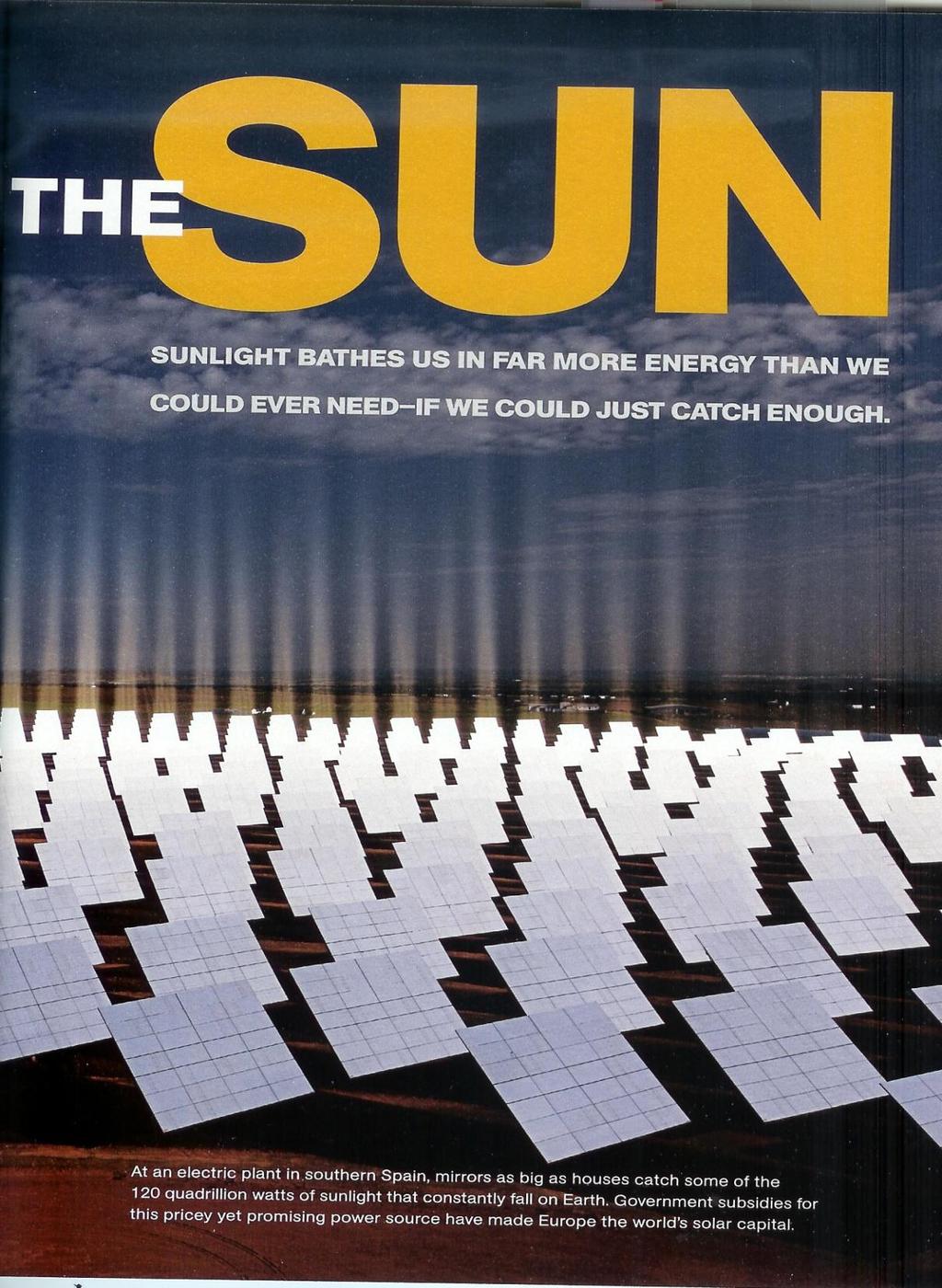
7 Background and Cost Photovoltaics convert sunlight directly to electric power Carbon-neutral Highly abundant the earth receives 120 quadrillion watts of power from the sun, humans currently use about 13 trillion watts Costs Module cost Balance of system cost Power conditioning cost Lewis, et al. Basic Research Needs for Solar Energy Utilization. Currently about $0.30/kWh, a factor of 5-10 behind total cost of fossil fuel generation
8 Lecture 1 Semiconductors and Physics at the Nano-scale Electronic Properties of Solids: Free-electron Fermi gas Energy bands in solids Semiconductors and doping pn junctions Amorphous semiconductors Nano-scale Physics: Background Quantum confinement
9
10
11 Review of Electronic Properties of Solids Free Electron Fermi Gas
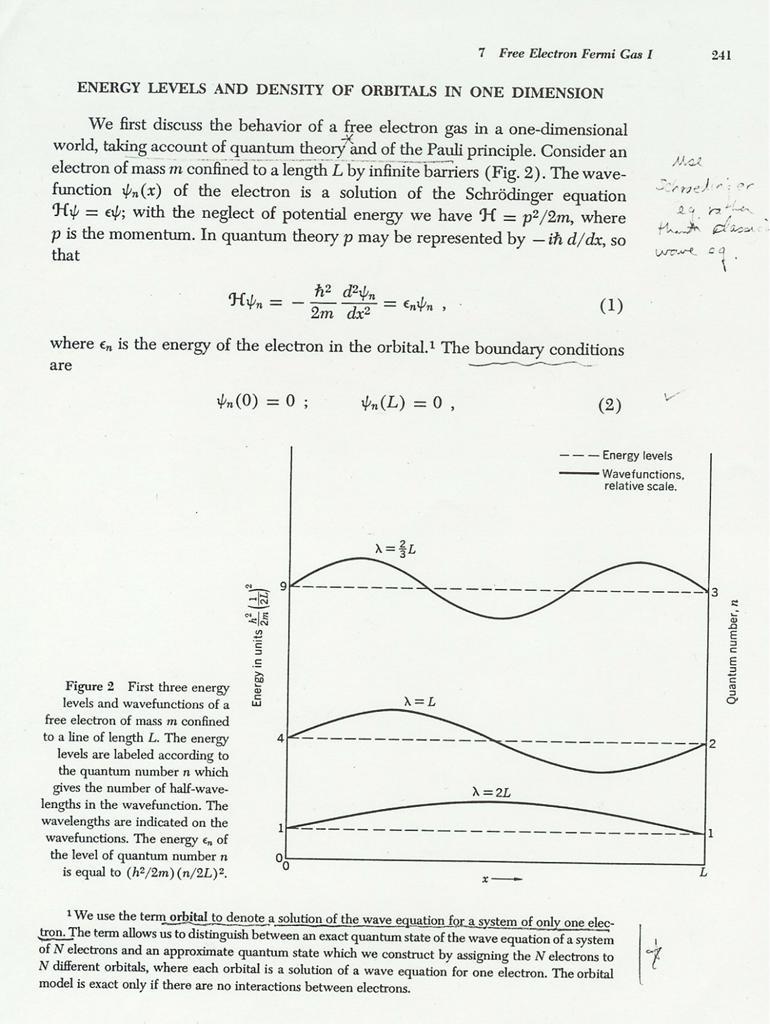
12
13
14
15 Energy Bands, Semiconductors, Doping
16 Hydrogen Molecule
17
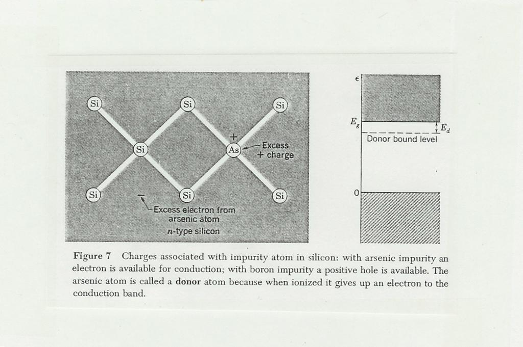
18
19 energy-states energy-states in solids: Band-Pattern Atom Molecule/Solid Clemson Summer School Dr. Karl Molter / FH Trier / molter@fhtrier.de 19
20 energy-states in solids: Insulator electron-energy conduction-band Clemson Summer School Dr. Karl Molter / FH Trier / molter@fhtrier.de Fermilevel E F bandgap E G (> 5 ev) valence-band
21
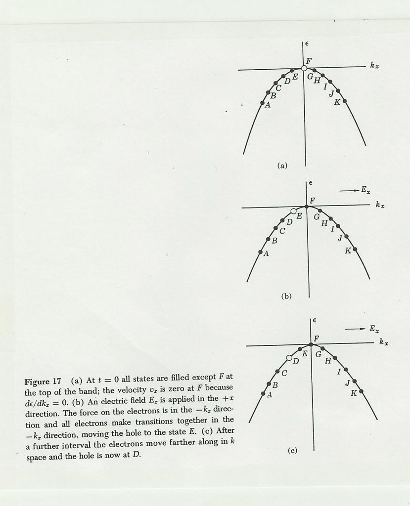
22 Figure 7.1. Schematic plot of the single particle energy spectrum in a bulk semiconductor for both the electron and hole states on the left side of the panel with appropriate electron (e) and hole (h) discrete quantum states shown on the right. The upper parabolic band is the conduction band, the lower the valence.
23
24 Figure A valence electron jumping across the energy gap in pure silicon resulting in the generation of a free electron and hole in the crystal: (a) energy band model, (b) bond model.
25 Figure Extrinsic n-type silicon doped with P donor atoms. (a) Energy band diagram and (b) Bond model.
26 Figure Extrinsic p-type silicon doped with B acceptor atoms. (a) Energy band diagram and (b) Bond model.
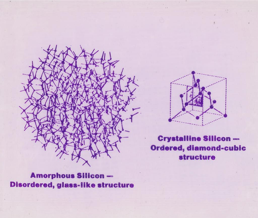
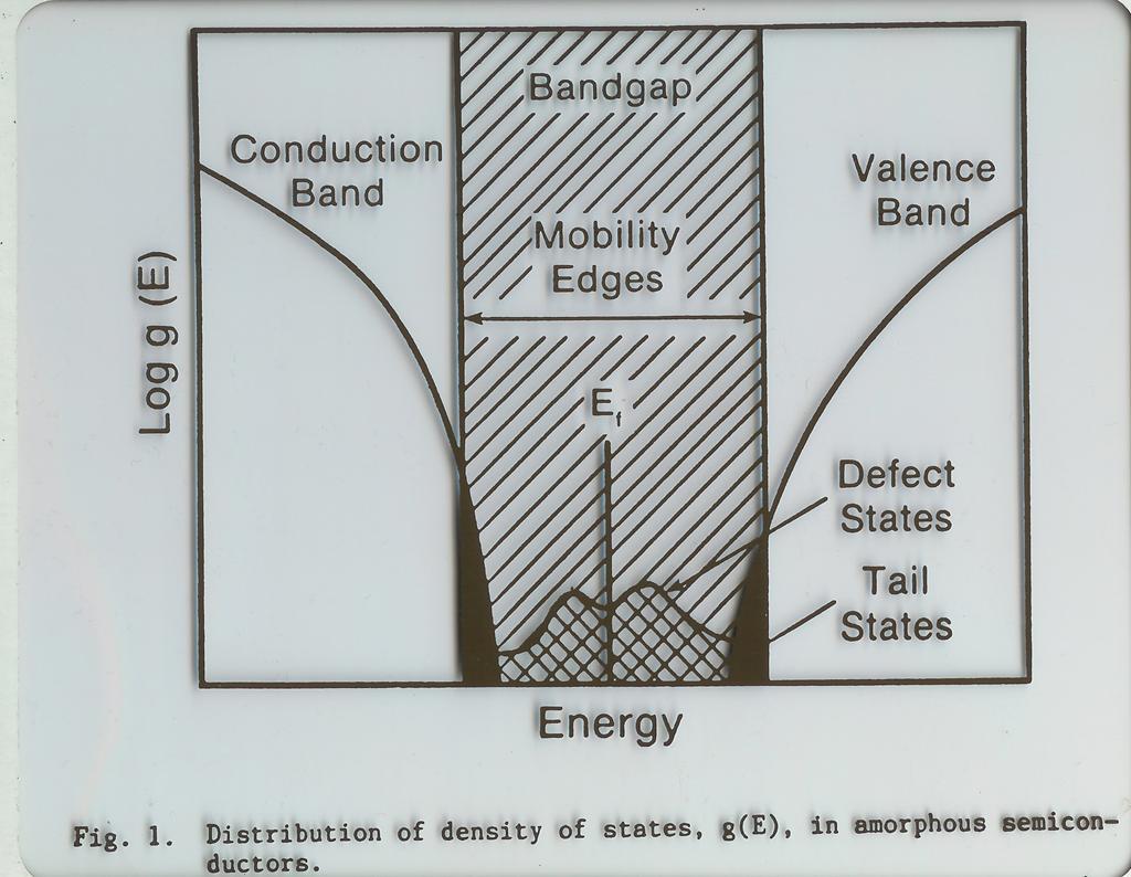
27
28 energy-states in solids : metal / conductor electron-energy Clemson Summer School Dr. Karl Molter / FH Trier / molter@fhtrier.de Fermilevel E F conduction-band
29 energy-states in solids: semiconductor electron-energy conduction-band Clemson Summer School Dr. Karl Molter / FH Trier / molter@fhtrier.de Fermilevel E F bandgap E G ( 0,5 2 ev) valence-band
30
31 Introduction to pn Junctions
32
33
34 Amorphous Semiconductors
35
36
37
38 Nanoscale Physics Background
39 10,000 Kilometers
40 1000 Kilometers
41 100 Kilometers

42 10 Kilometers
43 10 Kilometers

44 1 Kilometer

45 Oak trees 100 Meters
46
47
48
49
50
51
52
53
54
55
56
57 What is Nanotechnology? Research and technology development at the atomic, molecular or macromolecular levels, in the length scale of approximately nanometers. Creating and using structures, devices and systems that have novel properties and functions because of their small and/or intermediate size. Ability to control processes at a few nm-range for advanced material processing and manufacturing.


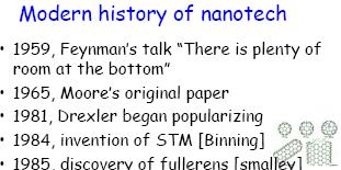
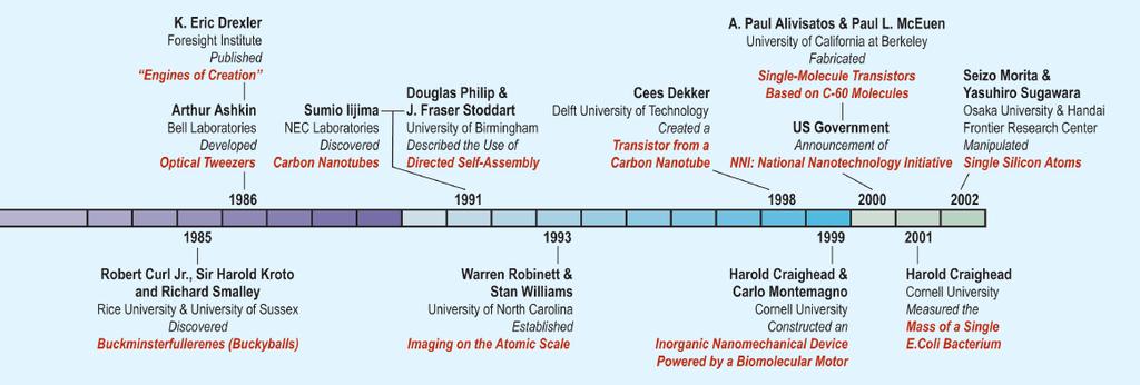
58 History of Nanotechnology As early as 500 AD, glass artisans were making stained glass windows with vibrant reds and yellows. These colours were much more luminous and durable than dyes could produce, and were the products of coinage metal nanoparticles imbedded in the glass. As these nanoparticles get smaller, the colours shift from red, through yellow and green, to blue. 58

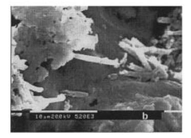
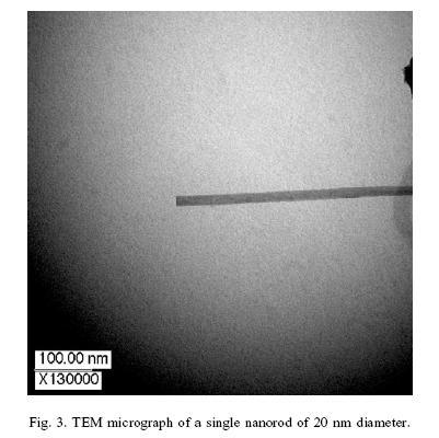
59
60
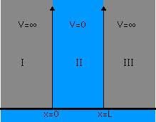
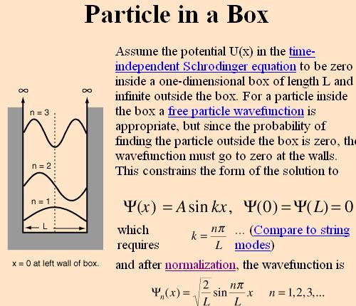
61
62


 devices 10-100 mm")


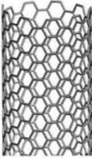
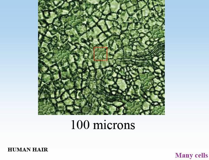
63 Soft x-ray Nanoworld Microworld Ultraviolet Visible Infrared Microwave The Scale of Things Nanometers and More Things Natural 10-2 m 1 cm 10 mm Things Manmade Head of a pin 1-2 mm The Challenge Ant ~ 5 mm 10-3 m 1,000,000 nanometers = 1 millimeter (mm) Dust mite 200 mm 10-4 m 0.1 mm 100 mm MicroElectroMechanical (MEMS) devices mm wide Human hair ~ mm wide Red blood cells (~7-8 mm) Fly ash ~ mm 10-5 m 10-6 m 0.01 mm 10 mm 1,000 nanometers = 1 micrometer (mm) Pollen grain Red blood cells Zone plate x-ray lens Outer ring spacing ~35 nm O O S P O O O O O O O O O O O O O O O O O O O O O S S S S S S S 10-7 m 0.1 mm 100 nm Fabricate and combine nanoscale building blocks to make useful devices, e.g., a photosynthetic reaction center with integral semiconductor storage. ~10 nm diameter ATP synthase 10-8 m 0.01 mm 10 nm Self-assembled, Nature-inspired structure Many 10s of nm Nanotube electrode DNA ~2-1/2 nm diameter Atoms of silicon spacing ~tenths of nm 10-9 m m 1 nanometer (nm) 0.1 nm Quantum corral of 48 iron atoms on copper surface positioned one at a time with an STM tip Corral diameter 14 nm Carbon buckyball ~1 nm diameter Carbon nanotube ~1.3 nm diameter
64
65

66 20 nm nanorods of MnO 2 for positive electrodes in Li ion batteries
67
68 Quantum Confinement One Dimension
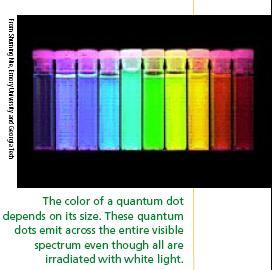
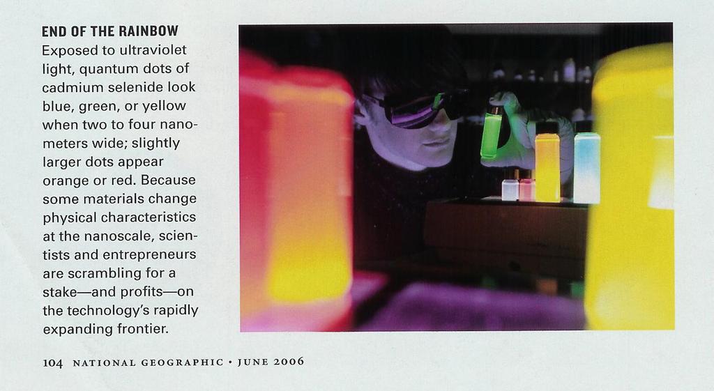
69
70
71
72
73
74 Quantum Confinement Three Dimensions
75
76

77 Figure 7.2. Solutions of quantum dots of varying size. Note the variation in color of each solution illustrating the particle size dependence of the optical absorption for each sample. Note that the smaller particles are in the red solution (absorbs blue), and that the larger ones are in the blue (absorbs red).
78
79
80
81
82
83
84
85
86
87
672 Advanced Solid State Physics. Scanning Tunneling Microscopy
 672 Advanced Solid State Physics Scanning Tunneling Microscopy Biao Hu Outline: 1. Introduction to STM 2. STM principle & working modes 3. STM application & extension 4. STM in our group 1. Introduction
Nanotubes and Nanowires - One-dimensional Materials
 NCLT July 13th, 2006 Nanotubes and Nanowires - One-dimensional Materials Tim Sands Materials Engineering and Electrical & Computer Engineering Birck Nanotechnology Center Purdue University 100 nm Si/SiGe
Electrons are shared in covalent bonds between atoms of Si. A bound electron has the lowest energy state.
 Photovoltaics Basic Steps the generation of light-generated carriers; the collection of the light-generated carriers to generate a current; the generation of a large voltage across the solar cell; and
Lecture 1. OUTLINE Basic Semiconductor Physics. Reading: Chapter 2.1. Semiconductors Intrinsic (undoped) silicon Doping Carrier concentrations
 silicon Doping Carrier concentrations") Lecture 1 OUTLINE Basic Semiconductor Physics Semiconductors Intrinsic (undoped) silicon Doping Carrier concentrations Reading: Chapter 2.1 EE105 Fall 2007 Lecture 1, Slide 1 What is a Semiconductor? Low
Lecture 1 OUTLINE Basic Semiconductor Physics Semiconductors Intrinsic (undoped) silicon Doping Carrier concentrations Reading: Chapter 2.1 EE105 Fall 2007 Lecture 1, Slide 1 What is a Semiconductor? Low
PHY313 - CEI544 The Mystery of Matter From Quarks to the Cosmos Fall 2005
 PHY313 - CEI544 The Mystery of Matter From Quarks to the Cosmos Fall 2005 Peter Paul Office Physics D-143 www.physics.sunysb.edu then click on PHY313 or CEI544 Peter Paul 09/1/05 PHY313-CEI544 Fall-05
Nanotechnology and Solar Energy. Solar Electricity Photovoltaics. Fuel from the Sun Photosynthesis Biofuels Split Water Fuel Cells
 Nanotechnology and Solar Energy Solar Electricity Photovoltaics Fuel from the Sun Photosynthesis Biofuels Split Water Fuel Cells Solar cell A photon from the Sun generates an electron-hole pair in a semiconductor.
Introduction to Photovoltaics
 INTRODUCTION Objectives Understand the photovoltaic effect. Understand the properties of light. Describe frequency and wavelength. Understand the factors that determine available light energy. Use software
Lecture 3b. Bonding Model and Dopants. Reading: (Cont d) Notes and Anderson 2 sections
 Notes and Anderson 2 sections") Lecture 3b Bonding Model and Dopants Reading: (Cont d) Notes and Anderson 2 sections 2.3-2.7 The need for more control over carrier concentration Without help the total number of carriers (electrons and
Lecture 3b Bonding Model and Dopants Reading: (Cont d) Notes and Anderson 2 sections 2.3-2.7 The need for more control over carrier concentration Without help the total number of carriers (electrons and
Nanotechnology. Gavin Lawes Department of Physics and Astronomy
 Nanotechnology Gavin Lawes Department of Physics and Astronomy Earth-Moon distance 4x10 8 m (courtesy NASA) Length scales (Part I) Person 2m Magnetic nanoparticle 5x10⁻⁹ m 10 10 m 10 5 m 1 m 10-5 m 10-10
ME 4875/MTE C/18. Introduction to Nanomaterials and Nanotechnology. Lecture 1 - Introduction
 ME 4875/MTE 575 - C/18 Introduction to Nanomaterials and Nanotechnology Lecture 1 - Introduction 1 Course Information Syllabus uploaded to Canvas Schedule: Lectures MT-RF 10:00-10:50 pm in Olin Hall 223
ME 4875/MTE C/16. Introduction to Nanomaterials and Nanotechnology. Lecture 1 - Introduction
 ME 4875/MTE 575 - C/16 Introduction to Nanomaterials and Nanotechnology Lecture 1 - Introduction 1 Course Information Syllabus uploaded to mywpi Schedule: Lectures MT-RF 2:00-2:50 pm in Salisbury Labs
Photovoltaic Energy Conversion. Frank Zimmermann
 Photovoltaic Energy Conversion Frank Zimmermann Solar Electricity Generation Consumes no fuel No pollution No greenhouse gases No moving parts, little or no maintenance Sunlight is plentiful & inexhaustible
EECS130 Integrated Circuit Devices
 EECS130 Integrated Circuit Devices Professor Ali Javey 8/30/2007 Semiconductor Fundamentals Lecture 2 Read: Chapters 1 and 2 Last Lecture: Energy Band Diagram Conduction band E c E g Band gap E v Valence
Semiconductor Devices and Circuits Fall Midterm Exam. Instructor: Dr. Dietmar Knipp, Professor of Electrical Engineering. Name: Mat. -Nr.
 Semiconductor Devices and Circuits Fall 2003 Midterm Exam Instructor: Dr. Dietmar Knipp, Professor of Electrical Engineering Name: Mat. -Nr.: Guidelines: Duration of the Midterm: 1 hour The exam is a closed
KATIHAL FİZİĞİ MNT-510
 KATIHAL FİZİĞİ MNT-510 YARIİLETKENLER Kaynaklar: Katıhal Fiziği, Prof. Dr. Mustafa Dikici, Seçkin Yayıncılık Katıhal Fiziği, Şakir Aydoğan, Nobel Yayıncılık, Physics for Computer Science Students: With
The Dielectric Function of a Metal ( Jellium )
") The Dielectric Function of a Metal ( Jellium ) Total reflection Plasma frequency p (10 15 Hz range) Why are Metals Shiny? An electric field cannot exist inside a metal, because metal electrons follow the
The Dielectric Function of a Metal ( Jellium ) Total reflection Plasma frequency p (10 15 Hz range) Why are Metals Shiny? An electric field cannot exist inside a metal, because metal electrons follow the
EECS143 Microfabrication Technology
 EECS143 Microfabrication Technology Professor Ali Javey Introduction to Materials Lecture 1 Evolution of Devices Yesterday s Transistor (1947) Today s Transistor (2006) Why Semiconductors? Conductors e.g
EE 446/646 Photovoltaic Devices I. Y. Baghzouz
 EE 446/646 Photovoltaic Devices I Y. Baghzouz What is Photovoltaics? First used in about 1890, the word has two parts: photo, derived from the Greek word for light, volt, relating to electricity pioneer
Chemistry Instrumental Analysis Lecture 8. Chem 4631
 Chemistry 4631 Instrumental Analysis Lecture 8 UV to IR Components of Optical Basic components of spectroscopic instruments: stable source of radiant energy transparent container to hold sample device
PHOTOVOLTAICS Fundamentals
 PHOTOVOLTAICS Fundamentals PV FUNDAMENTALS Semiconductor basics pn junction Solar cell operation Design of silicon solar cell SEMICONDUCTOR BASICS Allowed energy bands Valence and conduction band Fermi
Lecture 2 Solar Cell theory: pn junctions under Illumination Homojunctions Open-circuit voltage, short-circuit current, fill factor, IV curve,
 Lecture 2 Solar Cell theory: pn junctions under Illumination Homojunctions Open-circuit voltage, short-circuit current, fill factor, IV curve, Solar-toelectric Conversion Efficiency Carrier Generation
Plasmonics. The long wavelength of light ( μm) creates a problem for extending optoelectronics into the nanometer regime.
 creates a problem for extending optoelectronics into the nanometer regime.") Plasmonics The long wavelength of light ( μm) creates a problem for extending optoelectronics into the nanometer regime. A possible way out is the conversion of light into plasmons. They have much shorter
Plasmonics The long wavelength of light ( μm) creates a problem for extending optoelectronics into the nanometer regime. A possible way out is the conversion of light into plasmons. They have much shorter
Quantum Dot Solar Cells
 Quantum Dot Solar Cells 2 INTRODUCTION: As industrialization speeds up in developing and under-developed countries with an alarming rise in population, global power consumption has become a big question
CHAPTER 11 Semiconductor Theory and Devices
 CHAPTER 11 Semiconductor Theory and Devices 11.1 Band Theory of Solids 11.2 Semiconductor Theory 11.3 Semiconductor Devices 11.4 Nanotechnology It is evident that many years of research by a great many
Review of Optical Properties of Materials
 Review of Optical Properties of Materials Review of optics Absorption in semiconductors: qualitative discussion Derivation of Optical Absorption Coefficient in Direct Semiconductors Photons When dealing
Charge Carriers in Semiconductor
 Charge Carriers in Semiconductor To understand PN junction s IV characteristics, it is important to understand charge carriers behavior in solids, how to modify carrier densities, and different mechanisms
David J. Starling Penn State Hazleton PHYS 214
 Being virtually killed by a virtual laser in a virtual space is just as effective as the real thing, because you are as dead as you think you are. -Douglas Adams, Mostly Harmless David J. Starling Penn
EE143 Fall 2016 Microfabrication Technologies. Evolution of Devices
 EE143 Fall 2016 Microfabrication Technologies Prof. Ming C. Wu wu@eecs.berkeley.edu 511 Sutardja Dai Hall (SDH) 1-1 Evolution of Devices Yesterday s Transistor (1947) Today s Transistor (2006) 1-2 1 Why
CLASS 12th. Semiconductors
 CLASS 12th Semiconductors 01. Distinction Between Metals, Insulators and Semi-Conductors Metals are good conductors of electricity, insulators do not conduct electricity, while the semiconductors have
In the name of Allah
 In the name of Allah Nano chemistry- 4 th stage Lecture No. 1 History of nanotechnology 16-10-2016 Assistance prof. Dr. Luma Majeed Ahmed lumamajeed2013@gmail.com, luma.ahmed@uokerbala.edu.iq Nano chemistry-4
First-Hand Investigation: Modeling of Semiconductors
 perform an investigation to model the behaviour of semiconductors, including the creation of a hole or positive charge on the atom that has lost the electron and the movement of electrons and holes in
NANO TECHNOLOGY IN POLYMER SOLAR CELLS. Mayur Padharia, Hardik Panchal, Keval Shah, *Neha Patni, Shibu.G.Pillai
 NANO TECHNOLOGY IN POLYMER SOLAR CELLS Mayur Padharia, Hardik Panchal, Keval Shah, *Neha Patni, Shibu.G.Pillai Department of Chemical Engineering, Institute of Technology, Nirma University, S. G. Highway,
Section 2: The Science of Solar Energy
 Section 2: The Science of Solar Energy SECTION 2: THE SCIENCE OF SOLAR ENERGY Solar Radiation 9 Solar radiation outside the earth s atmosphere is called extraterrestrial radiation. On average the extraterrestrial
ELECTRONIC DEVICES AND CIRCUITS SUMMARY
 ELECTRONIC DEVICES AND CIRCUITS SUMMARY Classification of Materials: Insulator: An insulator is a material that offers a very low level (or negligible) of conductivity when voltage is applied. Eg: Paper,
Chapter 12 - Modern Materials
 Chapter 12 - Modern Materials 12.1 Semiconductors Inorganic compounds that semiconduct tend to have chemical formulas related to Si and Ge valence electron count of four. Semiconductor conductivity can
Challenges in to-electric Energy Conversion: an Introduction
 Challenges in Solar-to to-electric Energy Conversion: an Introduction Eray S. Aydil Chemical Engineering and Materials Science Department Acknowledgements: National Science Foundation Minnesota Initiative
Chapter 1. Solar energy conversion: from amorphous silicon to Dye-Sensitized Solar Cells. 1.1 Photovoltaic history.
 Chapter 1 Solar energy conversion: from amorphous silicon to Dye-Sensitized Solar Cells 1.1 Photovoltaic history. 1.2 Operation of traditional photovoltaic devices. 1.3 Thin film solar cells. 1.4 Multijunction
From here we define metals, semimetals, semiconductors and insulators
 Topic 11-1: Heat and Light for Intrinsic Semiconductors Summary: In this video we aim to discover how intrinsic semiconductors respond to heat and light. We first look at the response of semiconductors
Nanostructures. Lecture 13 OUTLINE
 Nanostructures MTX9100 Nanomaterials Lecture 13 OUTLINE -What is quantum confinement? - How can zero-dimensional materials be used? -What are one dimensional structures? -Why does graphene attract so much
Inorganic compounds that semiconduct tend to have an average of 4 valence electrons, and their conductivity may be increased by doping.
 Chapter 12 Modern Materials 12.1 Semiconductors Inorganic compounds that semiconduct tend to have an average of 4 valence electrons, and their conductivity may be increased by doping. Doping yields different
Electro - Principles I
 Electro - Principles I Page 10-1 Atomic Theory It is necessary to know what goes on at the atomic level of a semiconductor so the characteristics of the semiconductor can be understood. In many cases a
Electronic Circuits for Mechatronics ELCT 609 Lecture 2: PN Junctions (1)
") Electronic Circuits for Mechatronics ELCT 609 Lecture 2: PN Junctions (1) Assistant Professor Office: C3.315 E-mail: eman.azab@guc.edu.eg 1 Electronic (Semiconductor) Devices P-N Junctions (Diodes): Physical
Electronic Circuits for Mechatronics ELCT 609 Lecture 2: PN Junctions (1) Assistant Professor Office: C3.315 E-mail: eman.azab@guc.edu.eg 1 Electronic (Semiconductor) Devices P-N Junctions (Diodes): Physical
Qualitative Picture of the Ideal Diode. G.R. Tynan UC San Diego MAE 119 Lecture Notes
 Qualitative Picture of the Ideal Diode G.R. Tynan UC San Diego MAE 119 Lecture Notes Band Theory of Solids: From Single Attoms to Solid Crystals Isolated Li atom (conducting metal) Has well-defined, isolated
Engineering 2000 Chapter 8 Semiconductors. ENG2000: R.I. Hornsey Semi: 1
 Engineering 2000 Chapter 8 Semiconductors ENG2000: R.I. Hornsey Semi: 1 Overview We need to know the electrical properties of Si To do this, we must also draw on some of the physical properties and we
Introduction to Nanotechnology Chapter 5 Carbon Nanostructures Lecture 1
 Introduction to Nanotechnology Chapter 5 Carbon Nanostructures Lecture 1 ChiiDong Chen Institute of Physics, Academia Sinica chiidong@phys.sinica.edu.tw 02 27896766 Carbon contains 6 electrons: (1s) 2,
A. OTHER JUNCTIONS B. SEMICONDUCTOR HETEROJUNCTIONS -- MOLECULES AT INTERFACES: ORGANIC PHOTOVOLTAIC BULK HETEROJUNCTION DYE-SENSITIZED SOLAR CELL
 A. OTHER JUNCTIONS B. SEMICONDUCTOR HETEROJUNCTIONS -- MOLECULES AT INTERFACES: ORGANIC PHOTOVOLTAIC BULK HETEROJUNCTION DYE-SENSITIZED SOLAR CELL March 24, 2015 The University of Toledo, Department of
Nanomaterials - Quantum Dots, Nanowires and Nanotubes
 NCLT July 15th, 2005 Nanomaterials - Quantum Dots, Nanowires and Nanotubes 100 nm Tim Sands Materials Engineering and Electrical & Computer Engineering Birck Nanotechnology Center Purdue University Si/SiGe
VALLIAMMAI ENGINEERING COLLEGE
 VALLIAMMAI ENGINEERING COLLEGE SRM Nagar, Kattankulathur 603 203 DEPARTMENT OF PHYSICS QUESTION BANK II SEMESTER PH8252 - PHYSICS FOR INFORMATION SCIENCE (Common to CSE & IT) Regulation 2017 Academic Year
PRESENTED BY: PROF. S. Y. MENSAH F.A.A.S; F.G.A.A.S UNIVERSITY OF CAPE COAST, GHANA.
 SOLAR CELL AND ITS APPLICATION PRESENTED BY: PROF. S. Y. MENSAH F.A.A.S; F.G.A.A.S UNIVERSITY OF CAPE COAST, GHANA. OUTLINE OF THE PRESENTATION Objective of the work. A brief introduction to Solar Cell
ECE 442. Spring, Lecture -2
 ECE 442 Power Semiconductor Devices and Integrated circuits Spring, 2006 University of Illinois at Chicago Lecture -2 Semiconductor physics band structures and charge carriers 1. What are the types of
Semiconductors. Semiconductors also can collect and generate photons, so they are important in optoelectronic or photonic applications.
 Semiconductors Semiconducting materials have electrical properties that fall between true conductors, (like metals) which are always highly conducting and insulators (like glass or plastic or common ceramics)
Senior Project Thesis Senior Project Committee, Department of Physics, Case Western Reserve University
 Liquid Crystal Semiconductor Nanostructures Richard Metzger,Department of Physics, Case Western Reserve University Nick Lind, Department of Physics, Case Western Reserve University Professor K. Singer,
ESE370: Circuit-Level Modeling, Design, and Optimization for Digital Systems
 ESE370: Circuit-Level Modeling, Design, and Optimization for Digital Systems Lec 6: September 14, 2015 MOS Model You are Here: Transistor Edition! Previously: simple models (0 and 1 st order) " Comfortable
Nanotechnology Fabrication Methods.
 Nanotechnology Fabrication Methods. 10 / 05 / 2016 1 Summary: 1.Introduction to Nanotechnology:...3 2.Nanotechnology Fabrication Methods:...5 2.1.Top-down Methods:...7 2.2.Bottom-up Methods:...16 3.Conclusions:...19
Basic cell design. Si cell
 Basic cell design Si cell 1 Concepts needed to describe photovoltaic device 1. energy bands in semiconductors: from bonds to bands 2. free carriers: holes and electrons, doping 3. electron and hole current:
Processing of Semiconducting Materials Prof. Pallab Banerji Department of Material Science Indian Institute of Technology, Kharagpur
 Processing of Semiconducting Materials Prof. Pallab Banerji Department of Material Science Indian Institute of Technology, Kharagpur Lecture - 4 Doping in Semiconductors Good morning. Let us start with
Tuesday, December 11th. To be handed in both as a hard copy (in my mailbox in LGRT 1127A) and on SPARK (as a turnitin assignment).
 and on SPARK (as a turnitin assignment).") Tuesday, December 11th. Announcements. Homework 10 (paper/project topics, etc.) due on Thursday (last class). Final papers/projects will be due by 5PM on Friday, December 21st. To be handed in both as
Tuesday, December 11th. Announcements. Homework 10 (paper/project topics, etc.) due on Thursday (last class). Final papers/projects will be due by 5PM on Friday, December 21st. To be handed in both as
smal band gap Saturday, April 9, 2011
 small band gap upper (conduction) band empty small gap valence band filled 2s 2p 2s 2p hybrid (s+p)band 2p no gap 2s (depend on the crystallographic orientation) extrinsic semiconductor semi-metal electron
Bohr s Model, Energy Bands, Electrons and Holes
 Dual Character of Material Particles Experimental physics before 1900 demonstrated that most of the physical phenomena can be explained by Newton's equation of motion of material particles or bodies and
29: Nanotechnology. What is Nanotechnology? Properties Control and Understanding. Nanomaterials
 29: Nanotechnology What is Nanotechnology? Properties Control and Understanding Nanomaterials Making nanomaterials Seeing at the nanoscale Quantum Dots Carbon Nanotubes Biology at the Nanoscale Some Applications
Basic Semiconductor Physics
 6 Basic Semiconductor Physics 6.1 Introduction With this chapter we start with the discussion of some important concepts from semiconductor physics, which are required to understand the operation of solar
UNIT I: Electronic Materials.
 SIDDHARTH INSTITUTE OF ENGINEERING & TECHNOLOGY :: PUTTUR Siddharth Nagar, Narayanavanam Road 517583 QUESTION BANK (DESCRIPTIVE) Subject with Code: SEMICONDUCTOR PHYSICS (18HS0851) Course & Branch: B.Tech
Two-dimensional lattice
 1 Two-dimensional lattice a 1 *, k x k x = 0, k y = 0 X M a 2, y a 1, x Γ X a 2 *, k y k x = 0.5 a 1 *, k y = 0 k x = 0, k y = 0.5 a 2 * Γ k x = 0.5 a 1 *, k y = 0.5 a 2 * X X M k x = 0.25 a 1 *, k y =
5. Semiconductors and P-N junction
 5. Semiconductors and P-N junction Thomas Zimmer, University of Bordeaux, France Summary Learning Outcomes... 2 Physical background of semiconductors... 2 The silicon crystal... 2 The energy bands... 3
Semiconductor physics I. The Crystal Structure of Solids
 Lecture 3 Semiconductor physics I The Crystal Structure of Solids 1 Semiconductor materials Types of solids Space lattices Atomic Bonding Imperfection and doping in SOLIDS 2 Semiconductor Semiconductors
e - Galvanic Cell 1. Voltage Sources 1.1 Polymer Electrolyte Membrane (PEM) Fuel Cell
 Fuel Cell") Galvanic cells convert different forms of energy (chemical fuel, sunlight, mechanical pressure, etc.) into electrical energy and heat. In this lecture, we are interested in some examples of galvanic cells.
Galvanic cells convert different forms of energy (chemical fuel, sunlight, mechanical pressure, etc.) into electrical energy and heat. In this lecture, we are interested in some examples of galvanic cells.
Nanotechnology. Yung Liou P601 Institute of Physics Academia Sinica
 Nanotechnology Yung Liou P601 yung@phys.sinica.edu.tw Institute of Physics Academia Sinica 1 1st week Definition of Nanotechnology The Interagency Subcommittee on Nanoscale Science, Engineering and Technology
Solid State Device Fundamentals
 Solid State Device Fundamentals ENS 345 Lecture Course by Alexander M. Zaitsev alexander.zaitsev@csi.cuny.edu Tel: 718 982 2812 Office 4N101b 1 The free electron model of metals The free electron model
Module 1 Units 3,4,5
 Module 1 Units 3,4,5 1. What is matter? Anything that occupies space or has mass 2. What are the two general categories of substances? Elements and compounds 3. How many naturally occurring elements are
DO PHYSICS ONLINE ELECTRIC CURRENT FROM IDEAS TO IMPLEMENTATION ATOMS TO TRANSISTORS ELECTRICAL PROPERTIES OF SOLIDS
 DO PHYSICS ONLINE FROM IDEAS TO IMPLEMENTATION 9.4.3 ATOMS TO TRANSISTORS ELECTRICAL PROPERTIES OF SOLIDS ELECTRIC CURRENT Different substances vary considerably in their electrical properties. It is a
Atoms? All matters on earth made of atoms (made up of elements or combination of elements).
.") Chapter 1 Atoms? All matters on earth made of atoms (made up of elements or combination of elements). Atomic Structure Atom is the smallest particle of an element that can exist in a stable or independent
Chapter 1 Atoms? All matters on earth made of atoms (made up of elements or combination of elements). Atomic Structure Atom is the smallest particle of an element that can exist in a stable or independent
In today s lecture, we will cover:
 In today s lecture, we will cover: Metal and Metal oxide Nanoparticles Semiconductor Nanocrystals Carbon Nanotubes 1 Week 2: Nanoparticles Goals for this section Develop an understanding of the physical
EE301 Electronics I , Fall
 EE301 Electronics I 2018-2019, Fall 1. Introduction to Microelectronics (1 Week/3 Hrs.) Introduction, Historical Background, Basic Consepts 2. Rewiev of Semiconductors (1 Week/3 Hrs.) Semiconductor materials
The Electromagnetic Properties of Materials
 The Electromagnetic Properties of Materials Electrical conduction Metals Semiconductors Insulators (dielectrics) Superconductors Magnetic materials Ferromagnetic materials Others Photonic Materials (optical)
ESE370: Circuit-Level Modeling, Design, and Optimization for Digital Systems
 ESE370: Circuit-Level Modeling, Design, and Optimization for Digital Systems Lec 6: September 18, 2017 MOS Model You are Here: Transistor Edition! Previously: simple models (0 and 1 st order) " Comfortable
Lecture 7: Extrinsic semiconductors - Fermi level
 Lecture 7: Extrinsic semiconductors - Fermi level Contents 1 Dopant materials 1 2 E F in extrinsic semiconductors 5 3 Temperature dependence of carrier concentration 6 3.1 Low temperature regime (T < T
Charge Excitation. Lecture 4 9/20/2011 MIT Fundamentals of Photovoltaics 2.626/2.627 Fall 2011 Prof. Tonio Buonassisi
 Charge Excitation Lecture 4 9/20/2011 MIT Fundamentals of Photovoltaics 2.626/2.627 Fall 2011 Prof. Tonio Buonassisi 1 2.626/2.627 Roadmap You Are Here 2 2.626/2.627: Fundamentals Every photovoltaic device
Two-dimensional lattice
 Two-dimensional lattice a 1 *, k x k x =0,k y =0 X M a 2, y Γ X a 2 *, k y a 1, x Reciprocal lattice Γ k x = 0.5 a 1 *, k y =0 k x = 0, k y = 0.5 a 2 * k x =0.5a 1 *, k y =0.5a 2 * X X M k x = 0.25 a 1
High efficiency silicon and perovskite-silicon solar cells for electricity generation
 High efficiency silicon and perovskite-silicon solar cells for electricity generation Ali Dabirian Email: dabirian@ipm.ir 1 From Solar Energy to Electricity 2 Global accumulative PV installed In Iran it
Solutions for Assignment-8
 Solutions for Assignment-8 Q1. The process of adding impurities to a pure semiconductor is called: [1] (a) Mixing (b) Doping (c) Diffusing (d) None of the above In semiconductor production, doping intentionally
Electron Energy, E E = 0. Free electron. 3s Band 2p Band Overlapping energy bands. 3p 3s 2p 2s. 2s Band. Electrons. 1s ATOM SOLID.
 Electron Energy, E Free electron Vacuum level 3p 3s 2p 2s 2s Band 3s Band 2p Band Overlapping energy bands Electrons E = 0 1s ATOM 1s SOLID In a metal the various energy bands overlap to give a single
Goal for next generation solar cells: Efficiencies greater than Si with low cost (low temperature) processing
 processing") Multi-junction cells MBE growth > 40% efficient Expensive Single crystal Si >20% efficient expensive Thin film cells >10% efficient Less expensive Toxic materials Polymers
Multi-junction cells MBE growth > 40% efficient Expensive Single crystal Si >20% efficient expensive Thin film cells >10% efficient Less expensive Toxic materials Polymers
Semiconductor Theory and Devices
 Semiconductor Theory and Devices Band Theory of Solids Semiconductor Theory Semiconductor Devices Nanotechnology It is evident that many years of research by a great many people, both before and after
Introduction. Katarzyna Skorupska. Silicon will be used as the model material however presented knowledge applies to other semiconducting materials
 Introduction Katarzyna Skorupska Silicon will be used as the model material however presented knowledge applies to other semiconducting materials 2 June 26 Intrinsic and Doped Semiconductors 3 July 3 Optical
The Opto-Electronic Physics That Just Broke the Efficiency Record in Solar Cells
 The Opto-Electronic Physics That Just Broke the Efficiency Record in Solar Cells Solar Energy Mini-Series Jen-Hsun Huang Engineering Center Stanford, California Sept. 26, 2011 Owen D. Miller & Eli Yablonovitch
3.23 Electrical, Optical, and Magnetic Properties of Materials
 MIT OpenCourseWare http://ocw.mit.edu 3.23 Electrical, Optical, and Magnetic Properties of Materials Fall 2007 For information about citing these materials or our Terms of Use, visit: http://ocw.mit.edu/terms.
Transparent TiO 2 nanotube/nanowire arrays on TCO coated glass substrates: Synthesis and application to solar energy conversion
 Transparent TiO 2 nanotube/nanowire arrays on TCO coated glass substrates: Synthesis and application to solar energy conversion Craig A. Grimes Department of Electrical Engineering Center for Solar Nanomaterials
A. OTHER JUNCTIONS B. SEMICONDUCTOR HETEROJUNCTIONS -- MOLECULES AT INTERFACES: ORGANIC PHOTOVOLTAIC BULK HETEROJUNCTION DYE-SENSITIZED SOLAR CELL
 A. OTHER JUNCTIONS B. SEMICONDUCTOR HETEROJUNCTIONS -- MOLECULES AT INTERFACES: ORGANIC PHOTOVOLTAIC BULK HETEROJUNCTION DYE-SENSITIZED SOLAR CELL March 20, 2014 The University of Toledo, Department of
Lesson 4: Tools of the Nanosciences. Student Materials
 Lesson 4: Tools of the Nanosciences Student Materials Contents Black Box Lab Activity: Student Instructions and Worksheet Seeing and Building Small Things: Student Reading Seeing and Building Small Things:
UNIT - IV SEMICONDUCTORS AND MAGNETIC MATERIALS
 1. What is intrinsic If a semiconductor is sufficiently pure, then it is known as intrinsic semiconductor. ex:: pure Ge, pure Si 2. Mention the expression for intrinsic carrier concentration of intrinsic
Chapter 1 Overview of Semiconductor Materials and Physics
 Chapter 1 Overview of Semiconductor Materials and Physics Professor Paul K. Chu Conductivity / Resistivity of Insulators, Semiconductors, and Conductors Semiconductor Elements Period II III IV V VI 2 B
NANOSCIENCE: TECHNOLOGY AND ADVANCED MATERIALS
 UNIVERSITY OF SOUTHAMPTON PHYS6014W1 SEMESTER 2 EXAMINATIONS 2012-2013 NANOSCIENCE: TECHNOLOGY AND ADVANCED MATERIALS DURATION 120 MINS (2 Hours) This paper contains 8 questions Answer ALL questions in
Free Electron Model for Metals
 Free Electron Model for Metals Metals are very good at conducting both heat and electricity. A lattice of in a sea of electrons shared between all nuclei (moving freely between them): This is referred
Lecture Number - 01 Metals, Semiconductors and Insulators
 Electronic Materials, Devices and Fabrication Dr. S. Parasuraman Department of Metallurgical and Materials Engineering Indian Institute of Technology, Madras Lecture Number - 01 Metals, Semiconductors
Quantum Dot Technology for Low-Cost Space Power Generation for Smallsats
 SSC06-VI- Quantum Dot Technology for Low-Cost Space Power Generation for Smallsats Theodore G. DR Technologies, Inc. 7740 Kenamar Court, San Diego, CA 92020 (858)677-230 tstern@drtechnologies.com The provision
Figure 3.1 (p. 141) Figure 3.2 (p. 142)
 Figure 3.2 (p. 142)") Figure 3.1 (p. 141) Allowed electronic-energy-state systems for two isolated materials. States marked with an X are filled; those unmarked are empty. System 1 is a qualitative representation of a metal;
Figure 3.1 (p. 141) Allowed electronic-energy-state systems for two isolated materials. States marked with an X are filled; those unmarked are empty. System 1 is a qualitative representation of a metal;
TECHNICAL INFORMATION. Quantum Dot
 Quantum Dot Quantum Dot is the nano meter sized semiconductor crystal with specific optical properties originates from the phenomenon which can be explained by the quantum chemistry and quantum mechanics.
NANOTECHNOLOGY. Students will gain an understanding of nanoscale dimensions and nanotechnology.
 NANOTECHNOLOGY By Anna M. Waldron and Carl A. Batt, Nanobiotechnology Center, Cornell University Subjects: Nanotechnology, Chemistry, Physics Time: Two class periods (approximately 90 minutes) Objective:
Photovoltaics. Lecture 7 Organic Thin Film Solar Cells Photonics - Spring 2017 dr inż. Aleksander Urbaniak
 Photovoltaics Lecture 7 Organic Thin Film Solar Cells Photonics - Spring 2017 dr inż. Aleksander Urbaniak Barcelona, Spain Perpignan train station, France source: pinterest Why organic solar cells? 1.
Quantum Dots and Colors Worksheet Answers
 Quantum Dots and Colors Worksheet Answers Background Quantum dots are semiconducting nanoparticles that are able to confine electrons in small, discrete spaces. Also known as zero-dimensional electronic