Is Nanoelectronics the Future?
|
|
|
- Andra Atkins
- 5 years ago
- Views:
Transcription
1 Is Nanoelectronics the Future? By Anurag Srivastava Semiconductor Physics


2 Nano World

3
4 Nano: From the Greek nanos - meaning "dwarf, this prefix is used in the metric system to mean 10-9 or 1/1,000,000,000.


5 ww.mathworks.com Nanoscale? Fullerenes C 60 12,756 Km m 22 cm 0.7 nm 0.22 m m 10 millions times smaller 1 billion times smaller
6 Nano is Different: Size Matters Bulk Gold = Yellow Nano Gold = Red Quantum Dots for Imaging and Diagnostics Optical properties change with size. Depending on their size CdSe particles can appear green or red in colour. nanocrystals absorb all energies higher than their band gap, they can also be used as color converters. Sizes of biological molecules are also on the order of a few nanometers. 2 nm 5 nm Quantum dot size can be controlled during their synthesis


7 Why Is Nanotechnology So Cool? Bulk Gold mp = 1064 C Color = gold 1 nm gold particles mp = 700 C l max = 420 nm Color = brown-yellow 20 nm gold particles mp = ~1000 C l max = 521 nm Color = red 100 nm gold particles mp = ~1000 C l max = 575 nm Color = purple-pink
8 Nano- and Micro-domains


 devices 10-100 mm")


 10-6")


9 Soft x-ray Nanoworld Microworld Ultraviolet Visible Infrared Microwave The Scale of Things Nanometers and More Things Natural m cm 10 mm 10-3 m 1,000,000 nm = 1 mm Things Man made Head of a pin 1-2 mm Challenges Dust mite 200 mm Ant ~ 5 mm 10-4 m 0.1 mm 100 mm MicroElectroMechanical (MEMS) devices mm wide Human hair ~ mm wide Fly ash ~ mm 10-5 m 0.01 mm 10 mm O P O O O O O O O O O O O O O O Red blood cells (~7-8 mm) 10-6 m 1,000 nm = 1 (mm) Pollen grain Red blood cells Zone plate x-ray lens Outer ring spacing ~35 nm O S O S O S O S O S O S O S O S 10-7 m 0.1 mm 100 nm Fabricate and combine nanoscale building blocks to make useful devices, e.g., a photosynthetic reaction center with integral semiconductor storage. ~10 nm diameter ATP synthase 10-8 m 0.01 mm 10 nm Self-assembled, Nature-inspired structure Many 10s of nm Nanotube electrode DNA ~2-1/2 nm diameter Atoms of silicon spacing ~tenths of nm 10-9 m 1 nm ABV- m IIITM-Gwalior 0.1 nm (MP) Quantum India corral of 48 iron atoms on copper surface positioned one at a time with an STM tip Corral diameter 14 nm Carbon buckyball ~1 nm diameter Carbon nanotube ~1.3 nm diameter
10 Nanoscience is the study of phenomena and manipulations of materials at atomic(~ 0.5 nm), molecular (~1-5nm) and macromolecular (~5-100 nm) scales, where properties differ significantly from those of the bulk materials. Nanotechnology concerns design, characterization, production and application of structures, devices and systems by controlling shape and size at nanometer scale. Nanotechnology is the creation of functional materials, devices, and systems through control of matter on the nanometer (1 to 100 nm) length scale and the exploitation of novel properties and phenomena developed at that scale. Source: Nanoscience and nanotechnologies: opportunities and uncertainties, The Royal Society & the Royal Academy of Engineering, London-2004.
11 Nanoscience and Nanotechnology are truly interdisciplinary, where physicists, chemists, engineers, biologists, computer scientists, environmentalists, industrialists, and policy makers have to work together.


12 Nanoscience? When people talk about Nanoscience, they start by describing things in their own way Physicists and Material Scientists point to things like new nanocarbon materials: They effuse about nanocarbon s strength and electrical properties Graphene Carbon Nanotube C60 Buckminster Fullerene
13 Nanotechnology is Not just new products a new means of production Manufacturing systems that make more manufacturing systems exponential proliferation Vastly accelerated product improvement cheap rapid prototyping Affects all industries and economic sectors general-purpose technology Inexpensive raw materials, potentially negligible capital cost economic discontinuity Portable, desktop-size factories social disruption Impacts will cross borders global transformation

14 Nano-bio Biologists counter that nanocarbon is a recent discovery THEY VE been studying DNA and RNA for much longer (And are already using it to transform our world)
15 What is Nanoelectronics? Nanoelectronics refer to the use of nanotechnology on electronic components, especially transistors. Although the term nanotechnology is generally defined as utilizing technology less than 100 nm in size, nanoelectronics often refer to transistor devices that are so small that inter-atomic interactions and quantum mechanical properties need to be studied extensively. As a result, present transistors do not fall under this category, even though these devices are manufactured with 45 nm, 32 nm, or 22 nm technology. Semiconductor Physics
16 Is this technology new? In one sense there is nothing new Whether we knew it or not, every piece of technology has involved the manipulation of atoms at some level. Many existing technologies depend crucially on processes that take place on the nanometer scale. Ex: Photography & Catalysis Nanotechnology, like any other branch of science, is primarily concerned with understanding how nature works.
17 Why is this length scale so important? There are five reasons: 1. The wavelike properties of electrons inside matter are influenced by variations on the nanometer scale. By patterning matter on the nanometer length, it is possible to vary fundamental properties of materials (for instance, melting temperature, magnetization, charge capacity) without changing the chemical composition. 2. The systematic organization of matter on the nanometer length scale is a key feature of biological systems. Nanotechnology promises to allow us to place artificial components and assemblies inside cells, and to make new materials using the self-assembly methods of nature.
18 Why is this length scale so important? 3. Nanoscale components have very high surface areas, making them ideal for use in composite materials, reacting systems, drug delivery, and energy storage. 4. The finite size of material entities, as compared to the molecular scale, determine an increase of the relative importance of surface tension and local electromagnetic effects, making nanostructured materials harder and less brittle. 5. The interaction wavelength scales of various external wave phenomena become comparable to the material entity size, making materials suitable for various opto-electronic applications.
19 How Small We can make the grains? Because of high surface areas conventional powders methods reach their limits at 10-6 m (1 micron) Smaller particles can be made but special methods are needed!
20 Working at the nanoscale Working in the nanoworld was first proposed by Richard Feynman back in But it's only true in the last decade. The world of the ultra small, in practical terms, is a distant place. We can't see or touch it. Because, optical microscopes can't provide images of anything smaller than the wavelength of visible light (ie, nothing smaller than 380 nanometres).
21 Some Nano definitions Cluster A collection of units (atoms or reactive molecules) of up to about 50 units Colloids A stable liquid phase containing particles in the nm range. A colloid particle is one such nm particle. Nanoparticle A solid particle in the nm range that could be nonocrystalline, an aggregate of crystallites or a single crystallite Nanocrystal A solid particle that is a single crystal in the nanometer range
22 What is so special about nanoscale Atoms and molecules are generally less than a nm. Size-dependent properties Surface to volume ratio A 3 nm iron particle has 50% atoms on the surface A 10 nm particle 20% on the surface A 30 nm particle only 5% on the surface Not just size reduction but phenomena intrinsic to nanoscale Size confinement Dominance of interfacial phenomena Quantum mechanics New behavior at nanoscale is not necessarily predictable from what we know at macroscales


23 Nanostructures Noble Metal Nanoparticles Carbon Nanotubes Sun, Y.; Xia, Y. Science 2002, 298, Courtesy of the Van Duyne group CdSe Quantum Dots Baughman, R. H.; Zakhidov, A. A.; de Heer, W. A. Science 2002, 297, 787 Courtesy of Liza Babayon Vigolo, B; Penicuad, A.; Coulon, C.; Sauder, C.; Pailler, R Journey, C.; Bernier, P. Poulin, P. Science 2000, 290, 1331
24 Size Matters As the size of an object becomes smaller and smaller, approaching nanoscale, the surface molecules become increasingly important relative to internal molecules Because of the increasing proportion of surface molecules relative to internal molecules Thus, the surface properties of materials of nanoscale objects become more influential in determining the behavior of the objects And the influence of bulk properties is reduced
25 Properties vary with the size of the material (Bulk) Gold is a shiny yellow metal Nanoscopic gold, i.e. clusters of gold atoms measuring 1 nm across, appears red Bulk gold does not exhibit catalytic properties Au nanocrystal is an excellent low temperature catalyst. Therefore, if we can control the processes that make a nanoscopic material, then we can control the material s properties.
26 Size Dependent Properties Chemical properties reactivity, catalysis Thermal properties melting temperature Mechanical properties adhesion, capillary forces Optical properties absorption and scattering of light Electrical properties tunneling current Magnetic properties superparamagnetic effect
27 Some Size Effects: Atomic Bonding Two types of atomic bonds: 1. Primary bonds combining atoms into molecules 2. Secondary bonds attraction between molecules to form bulk materials Secondary bonds become more important for nanoscale objects because their shapes and properties depend on these secondary bonding forces Thus, material properties and behavior of nanoscale objects are different from those of much larger objects
28 Size Effects: Quantum Mechanics Branch of physics concerned with the notion that all forms of energy occur in discrete units when observed on a small enough scale Example: electricity is conducted in units of electrons Quantum mechanics are significant for nanoscale entities One implication: As microelectronic devices reach nanoscale, we approach the limits of technological feasibility of current fabrication processes for integrated circuits Properties of nanostructured materials are size dependant. Properties can be tuned simply by adjusting the size, shape or extent of agglomeration.
29 Unique Properties of Nanoscale Materials Quantum size effects result in unique mechanical, electronic, photonic, and magnetic properties of nanoscale materials Chemical reactivity of nanoscale materials greatly different from more macroscopic form, e.g., gold Vastly increased surface area per unit mass, e.g., upwards of 1000 m 2 per gram New chemical forms of common chemical elements, e.g., fullerenes, nanotubes of carbon, titanium oxide, zinc oxide, other layered compounds
30 Nanofabrication Top-down Approach Bottom-up Approach
31 Top-down vs Bottom-up Top-down techniques take a bulk material, machine it, modify it into the desired shape and product classic example is manufacturing of integrated circuits using a sequence of steps sush as crystal growth, lithography, deposition, etching, Chemical Mechanical Planarization, ion implantation (Microelectronic/Nanoelectronics Fabrication Approach) Bottom-up techniques build something from basic materials assembling from the atoms/molecules up not completely proven in manufacturing yet Examples: Self-assembly Sol-gel technology Deposition (old but is used to obtain nanotubes, nanowires, nanoscale films ) Manipulators (AFM, STM,.)

32 Top-down From large items to smaller ones. The most common method are electron beam lithography (EBL) and scanning probe lithography (SPL). The approach involves molding or etching materials into smaller components. Making IC? Starting with a thin sheet Si wafer, cleaned, coated, preferentially etched using highly focused optics in as many as 100 separate operations before the final IC is complete.

33 Bottom-up A general approach going from small items to bigger ones. Building larger, more complex objects by integration of smaller building blocks or components. The sketch shows the essence of bottom-up manufacturing. Self-assembly from the gaseous phase. Two principle vapor-phase technologies that are useful and widely practiced: molecular beam epitaxy (MBE) and vapor-deposition (PVD, CVD).
 Gold nanoparticles of different sizes used to produce different colors in")


34 History of Nanotechnology ~ 2000 Years Ago Sulfide nanocrystals used by Greeks and Romans to dye hair ~ 1000 Years Ago (Middle Ages) Gold nanoparticles of different sizes used to produce different colors in stained glass windows 1959 There is plenty of room at the bottom by R. Feynman 1974 Nanotechnology - Taniguchi uses the term nanotechnology for the first time 1981 IBM develops Scanning Tunneling Microscope 1985 Buckyball - Scientists at Rice University and University of Sussex discover C Engines of Creation - First book on nanotechnology by K. Eric Drexler. Atomic Force Microscope invented by Binnig, Quate and Gerbe 1989 IBM logo made with individual atoms 1993 Carbon nanotube discovered by S. Iijima 1999 Nanomedicine 1st nanomedicine book by R. Freitas 2000 National Nanotechnology Initiative launched 2010 Noble Prize to Graphene
35 Nanoscale Size Effect Realization of miniaturized devices and systems while providing more functionality Attainment of high surface area to volume ratio Manifestation of novel phenomena and properties, including changes in: - Physical Properties (e.g. melting point) - Chemical Properties (e.g. reactivity) - Electrical Properties (e.g. conductivity) - Mechanical Properties (e.g. strength) - Optical Properties (e.g. light emission)

36 Some Milestones Milestone - 1 In 1959, in APS lecture at California Institute of Technology, USA, Prof. Feymann said that: In great future, we can arrange the atoms, the way we want, devices will be made on atomic scale, materials will be with intelligence, the motors smaller than pin head will control every thing. Prof. R.P. Feynman Nobel Prize Winner
37 Milestone - 2 Today, Nanomaterials and Nanotechnology are at the center stage. Nanotechnology is regarded as a key Technology.

38 Milestone Moore s Law of continuous miniaturization has been a driver towards nanotechnology. Moore s Law states that number of active transistor elements per chip doubles every 18 months.


39

40 Transistor Scaling

41 Transistor Scaling and Research Roadmap

42 Milestone G. Bennig & H, Rohrer at IBM Zurich Laboratory developed the Scanning Tunneling Microscope. For surface studies 1984 G. Bennig developed the Atomic Force Microscope times powerful than STM


43 Milestone R. Smalley and H. Kroto, Robert F. Curl discovered fullerenes C 60 and jointly got Nobel Prize in Chemistry for this discovery in 1996.
 discovered single")
44 Milestone S. Iijima (NEC, Japan) discovered single walled carbon nanotube.
45 Milestone - 7 In the 1930s, Landau and Peierls (and Mermin, later)showed thermodynamics prevented 2-d crystals in free state. Melting temperature of thin films decreases rapidly with decreasing thickness. In 2004, experimental discovery of graphene- high quality 2-d crystals. The Nobel Price 2010 in physics has been awarded to two scientists at the Manchester University for discovering the graphene. Konstantin Novoselov and Andre Geim were born in Russia, then they moved to the Netherlands and finally joining the Manchester University.
46 Milestone 7 They came up with an experiment in 2004 when they used scotch tape and a block of carbon to strip oneatom thick layers of carbon. Their discoveries were amazing as the graphene layers were almost transparent, almost as strong as steel, great heat and electric conductors, and very stretchy. It has been considered the perfect material and nowadays it has enormous implications in electronic devices, however, they can also be used to study quantum mechanics among others.

47 Milestone 7
48 Opportunities Changed Behaviour of Nanomaterials When we decrease the size of a material its behaviour and properties changes drastically as the dimensions reach 100nm or so. The main reasons for this change in behaviour are an increased relative surface area increased chemical activity

49 Diamonds, Graphite, Fullerenes & Carbon Nanotubes

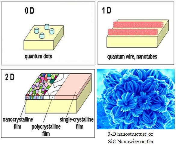
50 Carbon Nanotubes
51 Carbon Nanotubes
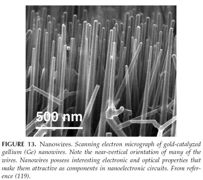
52 Nanowires

53 DNA Nanowires are the way out for connecting the transistors in the chip on a nanoscale. This is where DNA could come in as Metallic Nanowires.
54 Opportunities (contd.) Confining electrons within a space of a few nanometers causes them to exhibit quantum behaviour Discrete energy levels Changes in optical, magnetic and electrical properties. This provides us a basis for technologies for developing products with prescribed properties.

55 Self Organized Growth : Quantum Dot Self organized growth of semiconductor quantum dots A quantum dot A quantum dot is of semiconducting material with dimensions of the order of 10nm. A dot has an electronic energy level structure analogous to an atom and is also called an artificial atom.
56 Single Electron Transistor Quantum Dot Source Drain Conductance calculations Effect of Defects Quantum Dot Source Drain Defect
57 Type of nanomaterials


58 Why different properties at nanoscale? Quantum Confinement Surface to volume ratio
59 Quantum confinement is responsible for the increase of energy difference between energy states and band gap. A phenomenon tightly related with the optical and electronic properties of the materials. The quantum confinement effect can be observed once the diameter of the particle is of the same magnitude as the wavelength of the electron wave function. When materials are this small, their electronic and optical properties deviate substantially from those of bulk materials.
60 In order to understand quantum confinement, we need to go back to the very basics of quantum mechanics; namely the particle-in-a-box. All we need to worry about is, that the spacings between the energy levels increase as the length of the box decreases. Quantitatively, E n = n 2 h 2 /8mL 2. In the case of semiconductors this simply means that the band gap, starting from the bulk value, increases as the size of the nanocrystal decreases. In bulk solids the energy levels are closely spaced and thus form quasi-continuous bands. Going to the nano-regime the energy level separation increases and discrete energy levels are observed. Calculations on different systems show that quantum confinement effects are observable at sizes below 10 nm for most materials (~20 nm for Pb chalcogenides). Onset of confinement depends on a number of parameters such as the dielectric constant of the semiconductor and effective masses of the charge carriers.

61 Nanowires Nanowires: One-dimensional structures with two quantum confined directions and one unconfined direction for electrical conduction, which allows them to be used in various applications due to their unique electronic density of states. Nanowires: purely 1-D structures. Having widths or diameter tens of nm.

62 Nanowires: Year wise progress Yang et al. Nano Lett (2010)
63 Nanowires Applications Nanowires are subject of active research because IT industry is approaching the physical limits of conventional CMOS technology. Nanowires of GaN, AlN etc can be used for nano-leds. Nanowires of Si and Ge can be used for P-N junction Diodes. Use of nanowires as Solar cells Tian et al.nature 449, 885 (2007) Nanowires could be used to link tiny components into extremely small circuits. Quantum confinement in nanomaterials leads to quantum mechanical effects such as ballistic transport (Ballistic conduction or Ballistic transport is the transport of electrons in a medium with negligible electrical resistivity due to scattering. ) Realization of solar cells, efficient Li-ion batteries, sensors etc.
 Rice University scientists claim their miniscale wires are \"as small as such devices can possibly get,\" because each one comes complete with its")

64 Nanowires Applications Nanowire batteries now as 'small as possible,' could one day be included with nano toys. (Aug 4th 2011 ) Rice University scientists claim their miniscale wires are "as small as such devices can possibly get," because each one comes complete with its own anode, cathode and gel-like electrolyte coating Criss-crossed nanowires can compute (February 9 th 2011 Nature) Scientists have stitched together nanowires to create a microchip capable of basic computation. e-batteries-now-as-small-as-possible-couldone-day-be/ Researchers have used germanium wires to create a 'nanochip'
65 Nanoelectronic device? A very small devices to ovecome limits on scalability Examples: Single-Electron Transistors controlled electron tunneling to amplify current Resonance Tunneling Device quantum device use to control current
66 Problem of Making More Powerful Chips The number of transistors on a chip will approximately double every 18 to 24 months (Moore s Law). This law has given chip designers greater incentives to incorporate new features on silicon.
67 Problem of Making More Powerful Chips Moore's Law works largely through shrinking transistors, the circuits that carry electrical signals. By shrinking transistors, designers can squeeze more transistors into a chip.
68 Problem of Making More Powerful Chips However, more transistors means more electricity and heat compressed into a smaller space. Furthermore, smaller chips increase performance but also create the problem of complexity.
69 Problem of Making More Powerful Chips Band diagram when on A basic MOSFET
70 Problem of Making More Powerful Chips Quantum and coherence effects, high electric fields creating avalanche dielectric breakdowns, heat dissipation problems in closely packed structures as well as the nonuniformity of dopant atoms and the relevance of single atom defects are all roadblocks along the current road of miniaturization.
71 Problem of Making More Powerful Chips Problem 1: Carrier mobility decreases as channel length decrease and vertical electric fields increase.
72 Problem of Making More Powerful Chips Problem 2: Tunneling through gate oxide (off state current). E ox

73 Problem of Making More Powerful Chips Problem 3: Wattage/Area increases as density increases
74 Nanotechnology Potential Nanoparticles Nanomaterials Nanoelectronics Nanooptics Nanomagnetics Nanofluidics Nanobioelectronics
PV Tutorial Allen Hermann, Ph. D. Professor of Physics Emeritus, and Professor of Music Adjunct, University of Colorado, Boulder, Colorado, USA and
 PV Tutorial Allen Hermann, Ph. D. Professor of Physics Emeritus, and Professor of Music Adjunct, University of Colorado, Boulder, Colorado, USA and Vice-president, NanoTech Inc. Lexington, Kentucky, USA
Nanotechnology. Yung Liou P601 Institute of Physics Academia Sinica
 Nanotechnology Yung Liou P601 yung@phys.sinica.edu.tw Institute of Physics Academia Sinica 1 1st week Definition of Nanotechnology The Interagency Subcommittee on Nanoscale Science, Engineering and Technology
Nanotechnology Fabrication Methods.
 Nanotechnology Fabrication Methods. 10 / 05 / 2016 1 Summary: 1.Introduction to Nanotechnology:...3 2.Nanotechnology Fabrication Methods:...5 2.1.Top-down Methods:...7 2.2.Bottom-up Methods:...16 3.Conclusions:...19
In the name of Allah
 In the name of Allah Nano chemistry- 4 th stage Lecture No. 1 History of nanotechnology 16-10-2016 Assistance prof. Dr. Luma Majeed Ahmed lumamajeed2013@gmail.com, luma.ahmed@uokerbala.edu.iq Nano chemistry-4
672 Advanced Solid State Physics. Scanning Tunneling Microscopy
 672 Advanced Solid State Physics Scanning Tunneling Microscopy Biao Hu Outline: 1. Introduction to STM 2. STM principle & working modes 3. STM application & extension 4. STM in our group 1. Introduction
Nanostructures. Lecture 13 OUTLINE
 Nanostructures MTX9100 Nanomaterials Lecture 13 OUTLINE -What is quantum confinement? - How can zero-dimensional materials be used? -What are one dimensional structures? -Why does graphene attract so much
Seminars in Nanosystems - I
 Seminars in Nanosystems - I Winter Semester 2011/2012 Dr. Emanuela Margapoti Emanuela.Margapoti@wsi.tum.de Dr. Gregor Koblmüller Gregor.Koblmueller@wsi.tum.de Seminar Room at ZNN 1 floor Topics of the
Nanotechnology. Gavin Lawes Department of Physics and Astronomy
 Nanotechnology Gavin Lawes Department of Physics and Astronomy Earth-Moon distance 4x10 8 m (courtesy NASA) Length scales (Part I) Person 2m Magnetic nanoparticle 5x10⁻⁹ m 10 10 m 10 5 m 1 m 10-5 m 10-10
Like space travel and the Internet before it, the possibilities of the nano world catches the imagination of school children and scientists alike.
 The Nano World Preface Nano is the cool thing and it s the buzzword Like space travel and the Internet before it, the possibilities of the nano world catches the imagination of school children and scientists
Carbon Nanomaterials: Nanotubes and Nanobuds and Graphene towards new products 2030
 Carbon Nanomaterials: Nanotubes and Nanobuds and Graphene towards new products 2030 Prof. Dr. Esko I. Kauppinen Helsinki University of Technology (TKK) Espoo, Finland Forecast Seminar February 13, 2009
There's Plenty of Room at the Bottom
 There's Plenty of Room at the Bottom 12/29/1959 Feynman asked why not put the entire Encyclopedia Britannica (24 volumes) on a pin head (requires atomic scale recording). He proposed to use electron microscope
RAJASTHAN TECHNICAL UNIVERSITY, KOTA
 RAJASTHAN TECHNICAL UNIVERSITY, KOTA (Electronics & Communication) Submitted By: LAKSHIKA SOMANI E&C II yr, IV sem. Session: 2007-08 Department of Electronics & Communication Geetanjali Institute of Technical
Overview. Carbon in all its forms. Background & Discovery Fabrication. Important properties. Summary & References. Overview of current research
 Graphene Prepared for Solid State Physics II Pr Dagotto Spring 2009 Laurene Tetard 03/23/09 Overview Carbon in all its forms Background & Discovery Fabrication Important properties Overview of current
There s plenty of room at the bottom! - R.P. Feynman, Nanostructure: a piece of material with at least one dimension less than 100 nm in extent.
 Nanostructures and Nanotechnology There s plenty of room at the bottom! - R.P. Feynman, 1959 Materials behave differently when structured at the nm scale than they do in bulk. Technologies now exist that
1.1. Introduction to Nanoscience and Nanotechnology
 1.1. Introduction to Nanoscience and Nanotechnology 1.1.1. A Brief Historical Overview Before trying to understand and discuss about synthesis, characterization and application of nanomaterials, it is
Chapter 1 Introduction
 Chapter 1 Introduction A nanometer (nm) is one billionth (10-9 ) of a meter. Nanoscience can be defined as the science of objects and phenomena occurring at the scale of 1 to 100 nm. The range of 1 100
CHAPTER 11 Semiconductor Theory and Devices
 CHAPTER 11 Semiconductor Theory and Devices 11.1 Band Theory of Solids 11.2 Semiconductor Theory 11.3 Semiconductor Devices 11.4 Nanotechnology It is evident that many years of research by a great many
In today s lecture, we will cover:
 In today s lecture, we will cover: Metal and Metal oxide Nanoparticles Semiconductor Nanocrystals Carbon Nanotubes 1 Week 2: Nanoparticles Goals for this section Develop an understanding of the physical
Graphene. Tianyu Ye November 30th, 2011
 Graphene Tianyu Ye November 30th, 2011 Outline What is graphene? How to make graphene? (Exfoliation, Epitaxial, CVD) Is it graphene? (Identification methods) Transport properties; Other properties; Applications;
Final Reading Assignment: Travels to the Nanoworld: pages pages pages
 Final Reading Assignment: Travels to the Nanoworld: pages 152-164 pages 201-214 pages 219-227 Bottom-up nanofabrication Can we assemble nanomachines manually? What are the components (parts)? nanoparticles
CSCI 2570 Introduction to Nanocomputing
 CSCI 2570 Introduction to Nanocomputing The Emergence of Nanotechnology John E Savage Purpose of the Course The end of Moore s Law is in sight. Researchers are now exploring replacements for standard methods
PHYS 3313 Section 001 Lecture #21 Monday, Nov. 26, 2012
 PHYS 3313 Section 001 Lecture #21 Monday, Nov. 26, 2012 Superconductivity Theory, The Cooper Pair Application of Superconductivity Semi-Conductor Nano-technology Graphene 1 Announcements Your presentations
Nanotechnology Nanofabrication of Functional Materials. Marin Alexe Max Planck Institute of Microstructure Physics, Halle - Germany
 Nanotechnology Nanofabrication of Functional Materials Marin Alexe Max Planck Institute of Microstructure Physics, Halle - Germany Contents Part I History and background to nanotechnology Nanoworld Nanoelectronics
CH676 Physical Chemistry: Principles and Applications. CH676 Physical Chemistry: Principles and Applications
 CH676 Physical Chemistry: Principles and Applications History of Nanotechnology: Time Line Democritus in ancient Greece: concept of atom 1900 : Rutherford : discovery of atomic nucleus The first TEM was
Lesson 4: Tools of the Nanosciences. Student Materials
 Lesson 4: Tools of the Nanosciences Student Materials Contents Black Box Lab Activity: Student Instructions and Worksheet Seeing and Building Small Things: Student Reading Seeing and Building Small Things:
Physics and Material Science of Semiconductor Nanostructures
 Physics and Material Science of Semiconductor Nanostructures PHYS 570P Prof. Oana Malis Email: omalis@purdue.edu Course website: http://www.physics.purdue.edu/academic_programs/courses/phys570p/ 1 Course
Nanotubes and Nanowires - One-dimensional Materials
 NCLT July 13th, 2006 Nanotubes and Nanowires - One-dimensional Materials Tim Sands Materials Engineering and Electrical & Computer Engineering Birck Nanotechnology Center Purdue University 100 nm Si/SiGe
Carbon based Nanoscale Electronics
 Carbon based Nanoscale Electronics 09 02 200802 2008 ME class Outline driving force for the carbon nanomaterial electronic properties of fullerene exploration of electronic carbon nanotube gold rush of
29: Nanotechnology. What is Nanotechnology? Properties Control and Understanding. Nanomaterials
 29: Nanotechnology What is Nanotechnology? Properties Control and Understanding Nanomaterials Making nanomaterials Seeing at the nanoscale Quantum Dots Carbon Nanotubes Biology at the Nanoscale Some Applications
Wafer-scale fabrication of graphene
 Wafer-scale fabrication of graphene Sten Vollebregt, MSc Delft University of Technology, Delft Institute of Mircosystems and Nanotechnology Delft University of Technology Challenge the future Delft University
Chapter 10. Nanometrology. Oxford University Press All rights reserved.
 Chapter 10 Nanometrology Oxford University Press 2013. All rights reserved. 1 Introduction Nanometrology is the science of measurement at the nanoscale level. Figure illustrates where nanoscale stands
Special Topics in Semiconductor Nanotechnology ECE 598XL
 Special Topics in Semiconductor Nanotechnology ECE 598XL Fall 2009 ECE 598XL Syllabus Overview: size matters Formation Process Characterization SOA device applications and potentials Homework or quizzes
Graphene films on silicon carbide (SiC) wafers supplied by Nitride Crystals, Inc.
 wafers supplied by Nitride Crystals, Inc.") 9702 Gayton Road, Suite 320, Richmond, VA 23238, USA Phone: +1 (804) 709-6696 info@nitride-crystals.com www.nitride-crystals.com Graphene films on silicon carbide (SiC) wafers supplied by Nitride Crystals,
9702 Gayton Road, Suite 320, Richmond, VA 23238, USA Phone: +1 (804) 709-6696 info@nitride-crystals.com www.nitride-crystals.com Graphene films on silicon carbide (SiC) wafers supplied by Nitride Crystals,
MRSEC. Refrigerator Magnet Activity Guide. Quick Reference Activity Guide. a) b) c) = north = south. Activity Materials
 b) c) = north = south. Activity Materials") MRSEC Refrigerator Magnet Activity Guide Quick Reference Activity Guide Activity Materials Refrigerator magnet with removable probe strip Magnetic field diagrams Starting Points One of the great breakthroughs
MRSEC Refrigerator Magnet Activity Guide Quick Reference Activity Guide Activity Materials Refrigerator magnet with removable probe strip Magnetic field diagrams Starting Points One of the great breakthroughs
From nanophysics research labs to cell phones. Dr. András Halbritter Department of Physics associate professor
 From nanophysics research labs to cell phones Dr. András Halbritter Department of Physics associate professor Curriculum Vitae Birth: 1976. High-school graduation: 1994. Master degree: 1999. PhD: 2003.
ME 4875/MTE C16. Introduction to Nanomaterials and Nanotechnology. Lecture 2 - Applications of Nanomaterials + Projects
 ME 4875/MTE 575 - C16 Introduction to Nanomaterials and Nanotechnology Lecture 2 - Applications of Nanomaterials + Projects 1 Project Teams of 4 students each Literature review of one application of nanotechnology
1. Introduction : 1.2 New properties:
 Nanodevices In Electronics Rakesh Kasaraneni(PID : 4672248) Department of Electrical Engineering EEL 5425 Introduction to Nanotechnology Florida International University Abstract : This paper describes
Materials. Definitions of nanotechnology. The term nanotechnology was invented by Professor Norio Taniguchi at the University of Tokyo in 1971.
 Materials Definitions of nanotechnology The term nanotechnology was invented by Professor Norio Taniguchi at the University of Tokyo in 1971. The original definition, translated into English Nano-technology'
Chapter 12 - Modern Materials
 Chapter 12 - Modern Materials 12.1 Semiconductors Inorganic compounds that semiconduct tend to have chemical formulas related to Si and Ge valence electron count of four. Semiconductor conductivity can
Molecular Electronics For Fun and Profit(?)
") Molecular Electronics For Fun and Profit(?) Prof. Geoffrey Hutchison Department of Chemistry University of Pittsburgh geoffh@pitt.edu July 22, 2009 http://hutchison.chem.pitt.edu Moore s Law: Transistor
Molecular Electronics For Fun and Profit(?) Prof. Geoffrey Hutchison Department of Chemistry University of Pittsburgh geoffh@pitt.edu July 22, 2009 http://hutchison.chem.pitt.edu Moore s Law: Transistor
Nanotechnology where size matters
 Nanotechnology where size matters J Emyr Macdonald Overview Ways of seeing very small things What is nanotechnology and why is it important? Building nanostructures What we can do with nanotechnology?
Nanoelectronics. Topics
 Nanoelectronics Topics Moore s Law Inorganic nanoelectronic devices Resonant tunneling Quantum dots Single electron transistors Motivation for molecular electronics The review article Overview of Nanoelectronic
Chapter 1 Introduction
 Chapter 1 Introduction In our planet carbon forms the basis of all organic molecules which makes it the most important element of life. It is present in over 95% of the known chemical compounds overall
Nanomaterials and their Optical Applications
 Nanomaterials and their Optical Applications Winter Semester 2013 Lecture 02 rachel.grange@uni-jena.de http://www.iap.uni-jena.de/multiphoton Lecture 2: outline 2 Introduction to Nanophotonics Theoretical
Plasmonics. The long wavelength of light ( μm) creates a problem for extending optoelectronics into the nanometer regime.
 creates a problem for extending optoelectronics into the nanometer regime.") Plasmonics The long wavelength of light ( μm) creates a problem for extending optoelectronics into the nanometer regime. A possible way out is the conversion of light into plasmons. They have much shorter
Plasmonics The long wavelength of light ( μm) creates a problem for extending optoelectronics into the nanometer regime. A possible way out is the conversion of light into plasmons. They have much shorter
Nano-mechatronics. Presented by: György BudaváriSzabó (X0LY4M)
") Nano-mechatronics Presented by: György BudaváriSzabó (X0LY4M) Nano-mechatronics Nano-mechatronics is currently used in broader spectra, ranging from basic applications in robotics, actuators, sensors,
Nano-mechatronics Presented by: György BudaváriSzabó (X0LY4M) Nano-mechatronics Nano-mechatronics is currently used in broader spectra, ranging from basic applications in robotics, actuators, sensors,
SPECIFIC USES OR APPLICATIONS OF NANOSTRUCTURES; MEASUREMENT OR ANALYSIS OF NANOSTRUCTURES; MANUFACTURE OR TREATMENT OF NANOSTRUCTURES
 CPC - B82Y - 2017.08 B82Y SPECIFIC USES OR APPLICATIONS OF NANOSTRUCTURES; MEASUREMENT OR ANALYSIS OF NANOSTRUCTURES; MANUFACTURE OR TREATMENT OF NANOSTRUCTURES Definition statement This place covers:
The Dielectric Function of a Metal ( Jellium )
") The Dielectric Function of a Metal ( Jellium ) Total reflection Plasma frequency p (10 15 Hz range) Why are Metals Shiny? An electric field cannot exist inside a metal, because metal electrons follow the
The Dielectric Function of a Metal ( Jellium ) Total reflection Plasma frequency p (10 15 Hz range) Why are Metals Shiny? An electric field cannot exist inside a metal, because metal electrons follow the
Self-study problems and questions Processing and Device Technology, FFF110/FYSD13
 Self-study problems and questions Processing and Device Technology, FFF110/FYSD13 Version 2016_01 In addition to the problems discussed at the seminars and at the lectures, you can use this set of problems
materials, devices and systems through manipulation of matter at nanometer scale and exploitation of novel phenomena which arise because of the
 Nanotechnology is the creation of USEFUL/FUNCTIONAL materials, devices and systems through manipulation of matter at nanometer scale and exploitation of novel phenomena which arise because of the nanometer
Halbleiter. Prof. Yong Lei. Prof. Thomas Hannappel.
 Halbleiter Prof. Yong Lei Prof. Thomas Hannappel yong.lei@tu-ilemnau.de thomas.hannappel@tu-ilmenau.de Important Events in Semiconductors History 1833 Michael Faraday discovered temperature-dependent conductivity
ME 4875/MTE C/18. Introduction to Nanomaterials and Nanotechnology. Lecture 1 - Introduction
 ME 4875/MTE 575 - C/18 Introduction to Nanomaterials and Nanotechnology Lecture 1 - Introduction 1 Course Information Syllabus uploaded to Canvas Schedule: Lectures MT-RF 10:00-10:50 pm in Olin Hall 223
Carbon nanomaterials. Gavin Lawes Wayne State University.
 Carbon nanomaterials Gavin Lawes Wayne State University glawes@wayne.edu Outline 1. Carbon structures 2. Carbon nanostructures 3. Potential applications for Carbon nanostructures Periodic table from bpc.edu
.Fritjaf Capra, The Tao of Physics
 Probing inside the atom and investigating its structure, science transcended the limits of our sensory imagination. From this point on, it could no longer rely with absolute certainty on logic and common
Investigating Nano-Space
 Name Partners Date Visual Quantum Mechanics The Next Generation Investigating Nano-Space Goal You will apply your knowledge of tunneling to understand the operation of the scanning tunneling microscope.
ME 4875/MTE C/16. Introduction to Nanomaterials and Nanotechnology. Lecture 1 - Introduction
 ME 4875/MTE 575 - C/16 Introduction to Nanomaterials and Nanotechnology Lecture 1 - Introduction 1 Course Information Syllabus uploaded to mywpi Schedule: Lectures MT-RF 2:00-2:50 pm in Salisbury Labs
General concept and defining characteristics of AFM. Dina Kudasheva Advisor: Prof. Mary K. Cowman
 General concept and defining characteristics of AFM Dina Kudasheva Advisor: Prof. Mary K. Cowman Overview Introduction History of the SPM invention Technical Capabilities Principles of operation Examples
MSN551 LITHOGRAPHY II
 MSN551 Introduction to Micro and Nano Fabrication LITHOGRAPHY II E-Beam, Focused Ion Beam and Soft Lithography Why need electron beam lithography? Smaller features are required By electronics industry:
Nanotechnology: Today and tomorrow
 Nanotechnology: Today and tomorrow Horst-Günter Rubahn NanoSYD Mads Clausen Instituttet Syddansk Universitet Alsion 2 6400 Sønderborg Agenda Alsion A bit about nano Nanoproducts Top down vs. bottom up
EN2912C: Future Directions in Computing Lecture 08: Overview of Near-Term Emerging Computing Technologies
 EN2912C: Future Directions in Computing Lecture 08: Overview of Near-Term Emerging Computing Technologies Prof. Sherief Reda Division of Engineering Brown University Fall 2008 1 Near-term emerging computing
1.0 Introduction. 1.1 Nanotechnology Historical Developments
 1.0 Introduction 1.1 Nanotechnology Historical Developments Around 370BC, Democritus a Greek philosopher developed the atomic theory of matter. Nano in GREEK means DWARF. The prefix nano means a billionth
SYLLABUS FINDING NANO Syllabus NanoSCI DISCOVERING NANOTECHNOLOGY AND CULTURE IN GERMANY
 1. Syllabus NanoSCI Course title: NanoSCI - Electronic Properties of Nanoengineered Materials Catalog description: Physics and technology of nanoengineered materials and devices. Semiconductor nanostructures.
Lectures Graphene and
 Lectures 15-16 Graphene and carbon nanotubes Graphene is atomically thin crystal of carbon which is stronger than steel but flexible, is transparent for light, and conducts electricity (gapless semiconductor).
554 Chapter 10 Liquids and Solids
 554 Chapter 10 Liquids and Solids above 7376 kpa, CO 2 is a supercritical fluid, with properties of both gas and liquid. Like a gas, it penetrates deep into the coffee beans; like a liquid, it effectively
Kavli Workshop for Journalists. June 13th, CNF Cleanroom Activities
 Kavli Workshop for Journalists June 13th, 2007 CNF Cleanroom Activities Seeing nm-sized Objects with an SEM Lab experience: Scanning Electron Microscopy Equipment: Zeiss Supra 55VP Scanning electron microscopes
Nanotechnology in Consumer Products
 Nanotechnology in Consumer Products June 17, 2015 October 31, 2014 The webinar will begin at 1pm Eastern Time Perform an audio check by going to Tools > Audio > Audio Setup Wizard Chat Box Chat Box Send
Nanotechnology? Source: National Science Foundation (NSF), USA
, USA") 2 2 Nanotechnology? Ability to work at the atomic, molecular and even sub-molecular levels in order to create and use material structures, devices and systems with new properties and functions Source:
2 2 Nanotechnology? Ability to work at the atomic, molecular and even sub-molecular levels in order to create and use material structures, devices and systems with new properties and functions Source:
Nanostrukturphysik (Nanostructure Physics)
") Nanostrukturphysik (Nanostructure Physics) Prof. Yong Lei & Dr. Huaping Zhao Fachgebiet Angewandte Nanophysik, Institut für Physik Contact: yong.lei@tu-ilmenau.de; huaping.zhao@tu-ilmenau.de Office: Unterpoerlitzer
Nanostrukturphysik (Nanostructure Physics) Prof. Yong Lei & Dr. Huaping Zhao Fachgebiet Angewandte Nanophysik, Institut für Physik Contact: yong.lei@tu-ilmenau.de; huaping.zhao@tu-ilmenau.de Office: Unterpoerlitzer
Introduction to Nanoscience and Nanotechnology
 Introduction to Nanoscience and Nanotechnology ENS 463 by Alexander M. Zaitsev alexander.zaitsev@csi.cuny.edu Tel: 718 982 2812 Office 4N101b 1 What is the size for a nano? 10-3 m, (milli) Macroobjects,
Scanning Probe Microscopy (SPM)
") http://ww2.sljus.lu.se/staff/rainer/spm.htm Scanning Probe Microscopy (FYST42 / FAFN30) Scanning Probe Microscopy (SPM) overview & general principles March 23 th, 2018 Jan Knudsen, room K522, jan.knudsen@sljus.lu.se
http://ww2.sljus.lu.se/staff/rainer/spm.htm Scanning Probe Microscopy (FYST42 / FAFN30) Scanning Probe Microscopy (SPM) overview & general principles March 23 th, 2018 Jan Knudsen, room K522, jan.knudsen@sljus.lu.se
Lecture 0: Introduction
 Lecture 0: Introduction Introduction q Integrated circuits: many transistors on one chip q Very Large Scale Integration (VLSI): bucketloads! q Complementary Metal Oxide Semiconductor Fast, cheap, low power
Information processing in nanoscale systems
 Information processing in nanoscale systems Mark Rudner Niels Bohr International Academy Image from: www.upscale.utoronto.ca 100 years after Bohr, the basic laws and players are established 1913 2013 Image
PHYS 3313 Section 001 Lecture #24 Monday, Apr. 21, 2014
 PHYS 3313 Section 001 Lecture #24 Monday, Apr. 21, 2014 Liquid Helium Superconductivity Theory, The Cooper Pair Application of Superconductivity Nano-technology Graphene 1 Announcements Reminder Homework
Modern physics. 4. Barriers and wells. Lectures in Physics, summer
 Modern physics 4. Barriers and wells Lectures in Physics, summer 016 1 Outline 4.1. Particle motion in the presence of a potential barrier 4.. Wave functions in the presence of a potential barrier 4.3.
V S I H S AK A HAPATNAM
 NANO MATERIALS K.SRIYOGI Assistant Professor Department of Industrial Production Engineering GITAM Institute Of Technology VISHAKHAPATNAM Nano technology-introduction: The emerging fields of nanoscience
Contents. Preface to the first edition
 Contents List of authors Preface to the first edition Introduction x xi xiii 1 The nanotechnology revolution 1 1.1 From micro- to nanoelectronics 2 1.2 From the macroscopic to the nanoscopic world 4 1.3
Graphene The Search For Two Dimensions. Christopher Scott Friedline Arizona State University
 Graphene The Search For Two Dimensions Christopher Scott Friedline Arizona State University What Is Graphene? Single atomic layer of graphite arranged in a honeycomb crystal lattice Consists of sp 2 -bonded
NANOSCIENCE AND NANOTECHNOLOGY
 NANOSCIENCE AND NANOTECHNOLOGY Yuehe Lin WHAT IS NANOTECHNOLOGY Nanotechnology is the understanding and control of matter at dimensions of roughly 1 to 100 nanometers, where unique phenomena enable novel
1. Nanotechnology & nanomaterials -- Functional nanomaterials enabled by nanotechnologies.
 Novel Nano-Engineered Semiconductors for Possible Photon Sources and Detectors NAI-CHANG YEH Department of Physics, California Institute of Technology 1. Nanotechnology & nanomaterials -- Functional nanomaterials
Nanomaterials. There is plenty of room at the bottom. Richard Feynman December 29th 1959
 Nanomaterials Chapter 1-1 There is plenty of room at the bottom Richard Feynman December 29th 1959 I would like to describe a field, in which little has been done, but in which an enormous amount can be
Nanocarbon Technology for Development of Innovative Devices
 Nanocarbon Technology for Development of Innovative Devices Shintaro Sato Daiyu Kondo Shinichi Hirose Junichi Yamaguchi Graphene, a one-atom-thick honeycomb lattice made of carbon, and a carbon nanotube,
Initial Stages of Growth of Organic Semiconductors on Graphene
 Initial Stages of Growth of Organic Semiconductors on Graphene Presented by: Manisha Chhikara Supervisor: Prof. Dr. Gvido Bratina University of Nova Gorica Outline Introduction to Graphene Fabrication
Image courtesy of Dr James Bendall, University of Cambridge, UK. Discover the secrets h of the Nanoworld
 Image courtesy of Dr James Bendall, University of Cambridge, UK. Discover the secrets h of the Nanoworld Nano has become a buzz word in popular culture to just mean small. To understand nanotechnology
Carbon Nanotubes: The Hub Of Nanoelectronics
 Carbon Nanotubes: The Hub Of Nanoelectronics P.I. Okwu 1 and I.N. Onyeje 2 1 Deputy Director, Electronics Development Institute (ELDI) Awka, Nigeria 2 Department of Electrical/Electronic Engineering, Anambra
Charge transport in molecular devices.
 Charge transport in molecular devices. Nanoscience and nanotechologies: new science? Nanoscience and nanotechnologies are fields of research that have attracted a lot of interest and large financing in
Recap (so far) Low-Dimensional & Boundary Effects
 Low-Dimensional & Boundary Effects") Recap (so far) Ohm s & Fourier s Laws Mobility & Thermal Conductivity Heat Capacity Wiedemann-Franz Relationship Size Effects and Breakdown of Classical Laws 1 Low-Dimensional & Boundary Effects Energy
Recap (so far) Ohm s & Fourier s Laws Mobility & Thermal Conductivity Heat Capacity Wiedemann-Franz Relationship Size Effects and Breakdown of Classical Laws 1 Low-Dimensional & Boundary Effects Energy
Chapter 12. Nanometrology. Oxford University Press All rights reserved.
 Chapter 12 Nanometrology Introduction Nanometrology is the science of measurement at the nanoscale level. Figure illustrates where nanoscale stands in relation to a meter and sub divisions of meter. Nanometrology
Techniken der Oberflächenphysik (Techniques of Surface Physics)
") Techniken der Oberflächenphysik (Techniques of Surface Physics) Prof. Yong Lei & Dr. Yang Xu Fachgebiet 3D-Nanostrukturierung, Institut für Physik Contact: yong.lei@tu-ilmenau.de yang.xu@tu-ilmenau.de
Techniken der Oberflächenphysik (Techniques of Surface Physics) Prof. Yong Lei & Dr. Yang Xu Fachgebiet 3D-Nanostrukturierung, Institut für Physik Contact: yong.lei@tu-ilmenau.de yang.xu@tu-ilmenau.de
News from NBIA. Condensed Matter Physics: from new materials to quantum technology. time. Mark Rudner
 News from NBIA Condensed Matter Physics: from new materials to quantum technology Mark Rudner time ~100 years after Bohr, the basic laws and players are established 1913 2013 Image from www.periodni.com
Nanobiotechnology. Place: IOP 1 st Meeting Room Time: 9:30-12:00. Reference: Review Papers. Grade: 40% midterm, 60% final report (oral + written)
") Nanobiotechnology Place: IOP 1 st Meeting Room Time: 9:30-12:00 Reference: Review Papers Grade: 40% midterm, 60% final report (oral + written) Midterm: 5/18 Oral Presentation 1. 20 minutes each person
Nanobiotechnology Place: IOP 1 st Meeting Room Time: 9:30-12:00 Reference: Review Papers Grade: 40% midterm, 60% final report (oral + written) Midterm: 5/18 Oral Presentation 1. 20 minutes each person
Nanostrukturphysik (Nanostructure Physics)
") Nanostrukturphysik (Nanostructure Physics) Prof. Yong Lei & Dr. Yang Xu Fachgebiet 3D-Nanostrukturierung, Institut für Physik Contact: yong.lei@tu-ilmenau.de; yang.xu@tu-ilmenau.de Office: Unterpoerlitzer
Nanostrukturphysik (Nanostructure Physics) Prof. Yong Lei & Dr. Yang Xu Fachgebiet 3D-Nanostrukturierung, Institut für Physik Contact: yong.lei@tu-ilmenau.de; yang.xu@tu-ilmenau.de Office: Unterpoerlitzer
Introduction to Nanotechnology Chapter 5 Carbon Nanostructures Lecture 1
 Introduction to Nanotechnology Chapter 5 Carbon Nanostructures Lecture 1 ChiiDong Chen Institute of Physics, Academia Sinica chiidong@phys.sinica.edu.tw 02 27896766 Carbon contains 6 electrons: (1s) 2,
NANOTECHNOLOGY. Students will gain an understanding of nanoscale dimensions and nanotechnology.
 NANOTECHNOLOGY By Anna M. Waldron and Carl A. Batt, Nanobiotechnology Center, Cornell University Subjects: Nanotechnology, Chemistry, Physics Time: Two class periods (approximately 90 minutes) Objective:
Ph.D. students, postdocs, and young researchers, which need to absorb a lot of new knowledge, not taught at universities, in a rather short time.
 We have started to work in the area of graphene at the end of 2006, discovering that the fascinating Dirac equations could drive to new discoveries in solid-state physics. At that time, although the Dirac
Graphene Fundamentals and Emergent Applications
 Graphene Fundamentals and Emergent Applications Jamie H. Warner Department of Materials University of Oxford Oxford, UK Franziska Schaffel Department of Materials University of Oxford Oxford, UK Alicja
National Science and Technology Council (NSTC) Committee on Technology
 Committee on Technology") BY LYNN YARRIS "The emerging fields of nanoscience and nanoengineering are leading to unprecedented understanding and control over the fundamental building blocks of all physical things. This is likely
BY LYNN YARRIS "The emerging fields of nanoscience and nanoengineering are leading to unprecedented understanding and control over the fundamental building blocks of all physical things. This is likely
LECTURE 1 : INTRODUCTION TO NANOMECHANICS
 I LECTURE 1 : INTRODUCTION TO NANOMECHANICS Outline : NANOTECHNOLOGY / NANOMECHANICS DEFINITIONS... 2 WHY IS NANO INTERESTING?... 3 HISTORY OF NANOTECHNOLOGY/NANOMECHANICS : TIME LINE... 4 The First Talk
Lecture 6: Individual nanoparticles, nanocrystals and quantum dots
 Lecture 6: Individual nanoparticles, nanocrystals and quantum dots Definition of nanoparticle: Size definition arbitrary More interesting: definition based on change in physical properties. Size smaller
Introduction to Scanning Probe Microscopy Zhe Fei
 Introduction to Scanning Probe Microscopy Zhe Fei Phys 590B, Apr. 2019 1 Outline Part 1 SPM Overview Part 2 Scanning tunneling microscopy Part 3 Atomic force microscopy Part 4 Electric & Magnetic force
Nanotechnology. An Introduction
 Nanotechnology An Introduction Nanotechnology A new interdisciplinary field of science The study of systems at the nanoscale The use of tools at the nanoscale Building and applying structures that are