Nanostructures. Lecture 13 OUTLINE
|
|
|
- Gary Carroll
- 5 years ago
- Views:
Transcription

1 Nanostructures MTX9100 Nanomaterials Lecture 13 OUTLINE -What is quantum confinement? - How can zero-dimensional materials be used? -What are one dimensional structures? -Why does graphene attract so much attention? 1


2 General characteristics of nanomaterial classes and their dimensionality 2 M. Ashby, P. Ferreira, D. Schodek; Nanomaterials, Nanotechnologies and Design; Copyright 2009 Elsevier Ltd.
3 Zero-dimensional materials Nanocrystals absorb light then reemit the light in a different color the size of the nanocrystal (at the Angstrom scale) determines the color. Six different quantum dot solutions are shown excited with a long wave UV lamp. 3 A quantum dot is a semiconductor whose excitons are confined in all three spatial dimensions. As a result, they have properties that are between those of bulk semiconductors and those of discrete molecules. The term "Quantum Dot" was coined by Mark Reed at Texas Instruments.
4 Quantum confinement in semiconductors In an unconfined (bulk) semiconductor, an electron-hole pair is typically bound within a characteristic length called the Bohr exciton radius. If the electron and hole are constrained further, then the semiconductor's properties change. This effect is a form of quantum confinement, and it is a key feature in many emerging electronic structures. Specifically, the effect describes the phenomenon results from electrons and electron holes being squeezed into a dimension that approaches a critical quantum measurement. 4 An exciton is a bound state of an electron and an imaginary particle called an electron hole in an insulator or semiconductor, and such is a Coulomb-correlated electron-hole pair.
5 Quantum confinement For 0-D nanomaterials, where all the dimensions are at the nanoscale, an electron is confined in 3-D space. Quantum confinement is responsible for the increase of energy difference between energy states and band gap. A phenomenon tightly related with the optical and electronic properties of the materials. 5 No electron delocalization (freedom to move) occurs.
6 Fundamentals of light Light is a form of electromagnetic (interacting electric and magnetic fields) radiant energy that propagates through space in a way that can be characterized as waves. Electromagnetic radiation can be defined in terms of its wavelength or frequency (reciprocals of one another). The electromagnetic spectrum is very large ranging, from wavelengths at the kilometer scale to those near the atomic scale. 6

7 Solid-state lighting The direct conversion of electricity to light using semiconductor materials (normally in the form of light emitted diodes - LEDs) LEDs fundamentally produce light via a special form of electroluminescence. One of the fundamental problems with LEDs that of narrow sets of emission frequencies that limit their uses is solvable via quantum dot technologies. 7 A new generation of solid-state lighting quantum light-emitting diodes (QLEDs) made of quantum dot networks are coming into use that would work similarly to traditional LEDs but have greatly improved functionalities and new uses.
8 Quantum dots Quantum dots offer great potential in the form of QLEDs which are made out of networks of quantum dots and can also build on, yet dramatically improve, existing LED technologies. Quantum dots are essentially nanometer-size crystals of semiconductor materials (e.g., silicon or germanium) for which the electronic properties are strongly dependent on their size. Wavelengths in quantum dots can be controlled in nanocrystalline materials. The energy separation between valence and conduction bands can be altered in nanocrystalline quantum dots by changing the size of the nanoparticles. Resulting energy levels can thus be varied. 8
 of a quantum dot of gallium arsenide, containing just 465 atoms.")
9 Making quantum dots quantum dot of gallium arsenide There are several ways to confine excitons in semiconductors, resulting in different methods to produce quantum dots. The total electron charge density (shown in green) of a quantum dot of gallium arsenide, containing just 465 atoms. (Image: Lin-Wang Wang) In general, quantum wires, wells and dots are grown by advanced epitaxial techniques in nanocrystals produced by chemical methods or by ion implantation, or in nanodevices made by stateof-the-art lithographic techniques 9
10 Applications Quantum dots are particularly significant for optical applications due to their theoretically high quantum yield. a measure of the efficiency with which absorbed light produces some effect. the probability that a given quantum state is formed from the system initially prepared in some other quantum state In electronic applications they have been proven to operate like a single-electron transistor and show the Coulomb blockade effect. Quantum dots have also been suggested as implementations of qubits for quantum information processing. the increased resistance at small bias voltages of an electronic device comprising at least one lowcapacitance tunnel junction. concerns information science that depends on quantum effects in physics 10
11 Quantum Dot infrared photodetectors AFM micrographs of: a 1 μm x 1 μm surface imaging of InAs quantum dots on GaAs/InP, (inset) a single InAs quantum dot. Researchers have demonstrated the self-assembled growth of In(Ga)As quantum dots in both InP-based and GaAs based systems using metalorganic chemical vapor deposition. 11 Such QDIPs have many advantages compared to the conventional quantum well infrared photodetector (QWIP), including: higher responsively, higher temperature operation, higher light coupling to normal incidence light, and capability of narrow band te nability.
12 The smallest nanostructures Nanotubes (1 - D): Long, cylindrical tubes of carbon formed by a catalytic growth process. Nanometer-scale drop of molten iron is typical catalyst. Can behave like a conductive metal wire or like a semiconductor Quantum dots (0 D): Crystals containing only a few hundred atoms Electrons are confined to widely separated energy levels -> dot emits one wavelength of light when excited Size of the dot determines electronic, magnetic, and optical properties Used as biological markers (illuminating sample with ultraviolet light crystals will fluoresce at a specific wavelength) 12
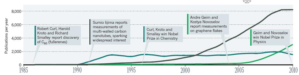
13 13 Carbon structures - publishing
; room")

14 One-dimensional nanomaterials TEM images of ZnO nanorods synthesized at different temperatures: 180C (a, b); room temperature (c); insets indicate crystal orientations. A photoluminescence spectrum of the room-temperature synthesized ZnO nanorods is displayed in (d). 14
 an as-prepared Cu nanowire")
 SAED pattern of the")
15 Nanostructures Solution synthesis of copper nanowires: (a) an as-prepared Cu nanowire suspension, (b) FESEM image of Cu nanowires, (c) TEM image of a Cu nanowire, and (d) SAED pattern of the nanowire in (c). 15
16 Nanowire nanosensors for biology Central to detection is the signal transduction associated with selective recognition of a biological or chemical species of interest. The diameters of the nanostructures are comparable to the sizes of biological and chemical species being sensed, and thus intuitively represent excellent primary transducers for producing signals that ultimately interface with macroscopic instruments. The size-tunable colors of semiconductor nanocrystals, together with their highly robust emission properties, are opening up opportunities for labelling and optical-based detection of biological species that offer advantages compared with conventional organic molecular dyes widely used today. 16
, the ubiquitous switches of the microelectronics industry.")

17 Nanowire field-effect sensors The underlying mechanism for nanowire sensors is a field effect that is transduced using fieldeffect transistors (FETs), the ubiquitous switches of the microelectronics industry. The electronic characteristics of nanowires are well controlled during growth in contrast to carbon nanotubes Si nanowires can be prepared as single-crystal structures with diameters as small as 2-3 nm a single Si nanowire sensor device 17


18 Two-dimensional nanomaterials 18 M. Ashby, P. Ferreira, D. Schodek; Nanomaterials, Nanotechnologies and Design; Copyright 2009 Elsevier Ltd.


19 Nanocoatings and multilayers 19 M. Ashby, P. Ferreira, D. Schodek; Nanomaterials, Nanotechnologies and Design; Copyright 2009 Elsevier Ltd.


20 Graphene The atomic structure of isolated, single-layer graphene: hexagonal lattice; high crystal quality 20


21 What is graphene? Band structure of graphene. The conductance band touches the valence band at the K and K points. charged massless particles (Dirac fermions) Charge carriers can travel thousands of interatomic distances without scattering Intrinsic graphene is a semi-metal or zero-gap semiconductor. 21


22 22 Graphite - Graphene Graphene is one-atom-thick planar sheet of sp 2 -bonded carbon atoms that are densely packed in a honeycomb crystal lattice. graphite itself consists of many graphene sheets stacked together The carbon-carbon bond length in graphene is about nm. Graphene is the basic structural element of some carbon allotropes including graphite, carbon nanotubes and fullerenes.
23 23 SCIENCE, June 2010 If there's a rock star in the world of materials, it's graphene: single-atom thick sheets of carbon prized for its off-the-charts ability to conduct electrons and for being all but transparent. Those qualities make graphene a tantalizing alternative for use as a transparent conductor, the sort now found in everything from computer displays and flat panel TVs to ATM touch screens and solar cells. But the material has been tough to manufacture in anything larger than flakes a few centimeters across. Now researchers have managed to create rectangular sheets of graphene 76 centimeters in the diagonal direction and even use them to create a working touchscreen display
24 Unique nature of charge carriers In condensed matter physics, the Schrodinger equation rules the world, usually being quite sufficient to describe electronic properties of materials. Graphene is an exception its charge carriers mimic relativistic particles and are more easily and naturally described starting with the Dirac equation rather than the Schrodinger equation. 24
25 Dirac fermions Although there is nothing particularly relativistic about electrons moving around carbon atoms, their interaction with the periodic potential of graphene s honeycomb lattice gives rise to new quasiparticles that at low energies E are accurately described by the Dirac equation with an effective speed of light. These quasi-particles, called massless Dirac fermions, can be seen as electrons that have lost their rest mass m or as neutrinos that acquired the electron charge e. The relativistic like description of electron waves on honeycomb lattices has been known theoretically for many years, never failing to attract attention, and the experimental discovery of graphene now provides a way to probe quantum electrodynamics (QED) phenomena by measuring graphene s electronic properties. 25
26 What kind of uses does graphene have? Graphene can be used to make excellent transistors. It is so thin we can easily control whether or not it conducts by applying an electric field. We would like to be able to do this with metals, but we cannot make metal films thin enough to affect their conducting state in this way. Electrons in graphene also travel ballistically over submicron distances. As a result, graphene-based transistors can run at higher frequencies and more efficiently than the silicon transistors we use now. At the present moment we have no way to produce entire integrated circuits from these transistors since we are limited by the size of graphenes we can produce. 26

27 Gas Sensors Gas molecules that land on graphene affect its electronic properties in a measurable way - in fact, we have measured the effect of a single molecule associating with a graphene. This means that we can create gas sensors which are sensitive to a single atom or molecule! 27


28 Example: how to make sensors bottom up 28

29 Thermal conductivity of thin CN films Thin films with oriented nanotube directions can have remarkably high thermal conductivities 29 M. Ashby, P. Ferreira, D. Schodek; Nanomaterials, Nanotechnologies and Design; Copyright 2009 Elsevier Ltd.
30 30 3-D nanomaterials


31 Opportunities for using nanomaterials and nanotechnologies in automobiles 31
Carbon based Nanoscale Electronics
 Carbon based Nanoscale Electronics 09 02 200802 2008 ME class Outline driving force for the carbon nanomaterial electronic properties of fullerene exploration of electronic carbon nanotube gold rush of
Nanomaterials and their Optical Applications
 Nanomaterials and their Optical Applications Winter Semester 2013 Lecture 02 rachel.grange@uni-jena.de http://www.iap.uni-jena.de/multiphoton Lecture 2: outline 2 Introduction to Nanophotonics Theoretical
Seminars in Nanosystems - I
 Seminars in Nanosystems - I Winter Semester 2011/2012 Dr. Emanuela Margapoti Emanuela.Margapoti@wsi.tum.de Dr. Gregor Koblmüller Gregor.Koblmueller@wsi.tum.de Seminar Room at ZNN 1 floor Topics of the
Chemistry Instrumental Analysis Lecture 8. Chem 4631
 Chemistry 4631 Instrumental Analysis Lecture 8 UV to IR Components of Optical Basic components of spectroscopic instruments: stable source of radiant energy transparent container to hold sample device
Chapter 3 Properties of Nanostructures
 Chapter 3 Properties of Nanostructures In Chapter 2, the reduction of the extent of a solid in one or more dimensions was shown to lead to a dramatic alteration of the overall behavior of the solids. Generally,
In today s lecture, we will cover:
 In today s lecture, we will cover: Metal and Metal oxide Nanoparticles Semiconductor Nanocrystals Carbon Nanotubes 1 Week 2: Nanoparticles Goals for this section Develop an understanding of the physical
PHYS 3313 Section 001 Lecture #21 Monday, Nov. 26, 2012
 PHYS 3313 Section 001 Lecture #21 Monday, Nov. 26, 2012 Superconductivity Theory, The Cooper Pair Application of Superconductivity Semi-Conductor Nano-technology Graphene 1 Announcements Your presentations
EN2912C: Future Directions in Computing Lecture 08: Overview of Near-Term Emerging Computing Technologies
 EN2912C: Future Directions in Computing Lecture 08: Overview of Near-Term Emerging Computing Technologies Prof. Sherief Reda Division of Engineering Brown University Fall 2008 1 Near-term emerging computing
3-month progress Report
 3-month progress Report Graphene Devices and Circuits Supervisor Dr. P.A Childs Table of Content Abstract... 1 1. Introduction... 1 1.1 Graphene gold rush... 1 1.2 Properties of graphene... 3 1.3 Semiconductor
In the name of Allah
 In the name of Allah Nano chemistry- 4 th stage Lecture No. 1 History of nanotechnology 16-10-2016 Assistance prof. Dr. Luma Majeed Ahmed lumamajeed2013@gmail.com, luma.ahmed@uokerbala.edu.iq Nano chemistry-4
Physics and Material Science of Semiconductor Nanostructures
 Physics and Material Science of Semiconductor Nanostructures PHYS 570P Prof. Oana Malis Email: omalis@purdue.edu Course website: http://www.physics.purdue.edu/academic_programs/courses/phys570p/ 1 Course
Graphene. Tianyu Ye November 30th, 2011
 Graphene Tianyu Ye November 30th, 2011 Outline What is graphene? How to make graphene? (Exfoliation, Epitaxial, CVD) Is it graphene? (Identification methods) Transport properties; Other properties; Applications;
Overview. Carbon in all its forms. Background & Discovery Fabrication. Important properties. Summary & References. Overview of current research
 Graphene Prepared for Solid State Physics II Pr Dagotto Spring 2009 Laurene Tetard 03/23/09 Overview Carbon in all its forms Background & Discovery Fabrication Important properties Overview of current
Electrical and Optical Properties. H.Hofmann
 Introduction to Nanomaterials Electrical and Optical Properties H.Hofmann Electrical Properties Ohm: G= σw/l where is the length of the conductor, measured in meters [m], A is the cross-section area of
ELECTRONIC DEVICES AND CIRCUITS SUMMARY
 ELECTRONIC DEVICES AND CIRCUITS SUMMARY Classification of Materials: Insulator: An insulator is a material that offers a very low level (or negligible) of conductivity when voltage is applied. Eg: Paper,
Designing Information Devices and Systems II A. Sahai, J. Roychowdhury, K. Pister Discussion 1A
 EECS 16B Spring 2019 Designing Information Devices and Systems II A. Sahai, J. Roychowdhury, K. Pister Discussion 1A 1 Semiconductor Physics Generally, semiconductors are crystalline solids bonded into
UNIT I: Electronic Materials.
 SIDDHARTH INSTITUTE OF ENGINEERING & TECHNOLOGY :: PUTTUR Siddharth Nagar, Narayanavanam Road 517583 QUESTION BANK (DESCRIPTIVE) Subject with Code: SEMICONDUCTOR PHYSICS (18HS0851) Course & Branch: B.Tech
1. Nanotechnology & nanomaterials -- Functional nanomaterials enabled by nanotechnologies.
 Novel Nano-Engineered Semiconductors for Possible Photon Sources and Detectors NAI-CHANG YEH Department of Physics, California Institute of Technology 1. Nanotechnology & nanomaterials -- Functional nanomaterials
Nanophysics: Main trends
 Nano-opto-electronics Nanophysics: Main trends Nanomechanics Main issues Light interaction with small structures Molecules Nanoparticles (semiconductor and metallic) Microparticles Photonic crystals Nanoplasmonics
GRAPHENE the first 2D crystal lattice
 GRAPHENE the first 2D crystal lattice dimensionality of carbon diamond, graphite GRAPHENE realized in 2004 (Novoselov, Science 306, 2004) carbon nanotubes fullerenes, buckyballs what s so special about
Nanotechnology. Yung Liou P601 Institute of Physics Academia Sinica
 Nanotechnology Yung Liou P601 yung@phys.sinica.edu.tw Institute of Physics Academia Sinica 1 1st week Definition of Nanotechnology The Interagency Subcommittee on Nanoscale Science, Engineering and Technology
Electrons are shared in covalent bonds between atoms of Si. A bound electron has the lowest energy state.
 Photovoltaics Basic Steps the generation of light-generated carriers; the collection of the light-generated carriers to generate a current; the generation of a large voltage across the solar cell; and
Lectures Graphene and
 Lectures 15-16 Graphene and carbon nanotubes Graphene is atomically thin crystal of carbon which is stronger than steel but flexible, is transparent for light, and conducts electricity (gapless semiconductor).
Halbleiter. Prof. Yong Lei. Prof. Thomas Hannappel.
 Halbleiter Prof. Yong Lei Prof. Thomas Hannappel yong.lei@tu-ilemnau.de thomas.hannappel@tu-ilmenau.de Important Events in Semiconductors History 1833 Michael Faraday discovered temperature-dependent conductivity
Graphene The Search For Two Dimensions. Christopher Scott Friedline Arizona State University
 Graphene The Search For Two Dimensions Christopher Scott Friedline Arizona State University What Is Graphene? Single atomic layer of graphite arranged in a honeycomb crystal lattice Consists of sp 2 -bonded
RAJASTHAN TECHNICAL UNIVERSITY, KOTA
 RAJASTHAN TECHNICAL UNIVERSITY, KOTA (Electronics & Communication) Submitted By: LAKSHIKA SOMANI E&C II yr, IV sem. Session: 2007-08 Department of Electronics & Communication Geetanjali Institute of Technical
Lecture 6: Individual nanoparticles, nanocrystals and quantum dots
 Lecture 6: Individual nanoparticles, nanocrystals and quantum dots Definition of nanoparticle: Size definition arbitrary More interesting: definition based on change in physical properties. Size smaller
TECHNICAL INFORMATION. Quantum Dot
 Quantum Dot Quantum Dot is the nano meter sized semiconductor crystal with specific optical properties originates from the phenomenon which can be explained by the quantum chemistry and quantum mechanics.
Lecture 1. Introduction to Electronic Materials. Reading: Pierret 1.1, 1.2, 1.4,
 Lecture 1 Introduction to Electronic Materials Reading: Pierret 1.1, 1.2, 1.4, 2.1-2.6 Atoms to Operational Amplifiers The goal of this course is to teach the fundamentals of non-linear circuit elements
Introduction to semiconductor nanostructures. Peter Kratzer Modern Concepts in Theoretical Physics: Part II Lecture Notes
 Introduction to semiconductor nanostructures Peter Kratzer Modern Concepts in Theoretical Physics: Part II Lecture Notes What is a semiconductor? The Fermi level (chemical potential of the electrons) falls
GRAPHENE NANORIBBONS Nahid Shayesteh,
 USC Department of Physics Graduate Seminar 1 GRAPHENE NANORIBBONS Nahid Shayesteh, Outlines 2 Carbon based material Discovery and innovation of graphen Graphene nanoribbons structure Application of Graphene
Chapter 1 Introduction
 Chapter 1 Introduction A nanometer (nm) is one billionth (10-9 ) of a meter. Nanoscience can be defined as the science of objects and phenomena occurring at the scale of 1 to 100 nm. The range of 1 100
Initial Stages of Growth of Organic Semiconductors on Graphene
 Initial Stages of Growth of Organic Semiconductors on Graphene Presented by: Manisha Chhikara Supervisor: Prof. Dr. Gvido Bratina University of Nova Gorica Outline Introduction to Graphene Fabrication
Fabrication / Synthesis Techniques
 Quantum Dots Physical properties Fabrication / Synthesis Techniques Applications Handbook of Nanoscience, Engineering, and Technology Ch.13.3 L. Kouwenhoven and C. Marcus, Physics World, June 1998, p.35
Black phosphorus: A new bandgap tuning knob
 Black phosphorus: A new bandgap tuning knob Rafael Roldán and Andres Castellanos-Gomez Modern electronics rely on devices whose functionality can be adjusted by the end-user with an external knob. A new
Carbon Nanomaterials: Nanotubes and Nanobuds and Graphene towards new products 2030
 Carbon Nanomaterials: Nanotubes and Nanobuds and Graphene towards new products 2030 Prof. Dr. Esko I. Kauppinen Helsinki University of Technology (TKK) Espoo, Finland Forecast Seminar February 13, 2009
Review of Optical Properties of Materials
 Review of Optical Properties of Materials Review of optics Absorption in semiconductors: qualitative discussion Derivation of Optical Absorption Coefficient in Direct Semiconductors Photons When dealing
Semiconductor Physics and Devices
 Syllabus Advanced Nano Materials Semiconductor Physics and Devices Textbook Donald A. Neamen (McGraw-Hill) Semiconductor Physics and Devices Seong Jun Kang Department of Advanced Materials Engineering
what happens if we make materials smaller?
 what happens if we make materials smaller? IAP VI/10 ummer chool 2007 Couvin Prof. ns outline Introduction making materials smaller? ynthesis how do you make nanomaterials? Properties why would you make
1. Introduction : 1.2 New properties:
 Nanodevices In Electronics Rakesh Kasaraneni(PID : 4672248) Department of Electrical Engineering EEL 5425 Introduction to Nanotechnology Florida International University Abstract : This paper describes
VALLIAMMAI ENGINEERING COLLEGE
 VALLIAMMAI ENGINEERING COLLEGE SRM Nagar, Kattankulathur 603 203 DEPARTMENT OF PHYSICS QUESTION BANK II SEMESTER PH8252 - PHYSICS FOR INFORMATION SCIENCE (Common to CSE & IT) Regulation 2017 Academic Year
From nanophysics research labs to cell phones. Dr. András Halbritter Department of Physics associate professor
 From nanophysics research labs to cell phones Dr. András Halbritter Department of Physics associate professor Curriculum Vitae Birth: 1976. High-school graduation: 1994. Master degree: 1999. PhD: 2003.
Nanoelectronics. Topics
 Nanoelectronics Topics Moore s Law Inorganic nanoelectronic devices Resonant tunneling Quantum dots Single electron transistors Motivation for molecular electronics The review article Overview of Nanoelectronic
Nanoscale optical circuits: controlling light using localized surface plasmon resonances
 Nanoscale optical circuits: controlling light using localized surface plasmon resonances T. J. Davis, D. E. Gómez and K. C. Vernon CSIRO Materials Science and Engineering Localized surface plasmon (LSP)
Electro - Principles I
 Electro - Principles I Page 10-1 Atomic Theory It is necessary to know what goes on at the atomic level of a semiconductor so the characteristics of the semiconductor can be understood. In many cases a
From Last Time Important new Quantum Mechanical Concepts. Atoms and Molecules. Today. Symmetry. Simple molecules.
 Today From Last Time Important new Quantum Mechanical Concepts Indistinguishability: Symmetries of the wavefunction: Symmetric and Antisymmetric Pauli exclusion principle: only one fermion per state Spin
Chapter 12 - Modern Materials
 Chapter 12 - Modern Materials 12.1 Semiconductors Inorganic compounds that semiconduct tend to have chemical formulas related to Si and Ge valence electron count of four. Semiconductor conductivity can
Electroluminescence from Silicon and Germanium Nanostructures
 Electroluminescence from silicon Silicon Getnet M. and Ghoshal S.K 35 ORIGINAL ARTICLE Electroluminescence from Silicon and Germanium Nanostructures Getnet Melese* and Ghoshal S. K.** Abstract Silicon
Chapter 1 Overview of Semiconductor Materials and Physics
 Chapter 1 Overview of Semiconductor Materials and Physics Professor Paul K. Chu Conductivity / Resistivity of Insulators, Semiconductors, and Conductors Semiconductor Elements Period II III IV V VI 2 B
CHAPTER 11 Semiconductor Theory and Devices
 CHAPTER 11 Semiconductor Theory and Devices 11.1 Band Theory of Solids 11.2 Semiconductor Theory 11.3 Semiconductor Devices 11.4 Nanotechnology It is evident that many years of research by a great many
OPTI510R: Photonics. Khanh Kieu College of Optical Sciences, University of Arizona Meinel building R.626
 OPTI510R: Photonics Khanh Kieu College of Optical Sciences, University of Arizona kkieu@optics.arizona.edu Meinel building R.626 Announcements HW#3 is assigned due Feb. 20 st Mid-term exam Feb 27, 2PM
Lecture 2. Semiconductor Physics. Sunday 4/10/2015 Semiconductor Physics 1-1
 Lecture 2 Semiconductor Physics Sunday 4/10/2015 Semiconductor Physics 1-1 Outline Intrinsic bond model: electrons and holes Charge carrier generation and recombination Intrinsic semiconductor Doping:
Conductivity and Semi-Conductors
 Conductivity and Semi-Conductors J = current density = I/A E = Electric field intensity = V/l where l is the distance between two points Metals: Semiconductors: Many Polymers and Glasses 1 Electrical Conduction
Graphene Novel Material for Nanoelectronics
 Graphene Novel Material for Nanoelectronics Shintaro Sato Naoki Harada Daiyu Kondo Mari Ohfuchi (Manuscript received May 12, 2009) Graphene is a flat monolayer of carbon atoms with a two-dimensional honeycomb
Introduction CHAPTER 01. Light and opto-semiconductors. Opto-semiconductor lineup. Manufacturing process of opto-semiconductors.
 CHAPTER 0 Light and opto-semiconductors - -2 Light Opto-semiconductors P. 0 P. 3 2 Opto-semiconductor lineup P. 5 3 Manufacturing process of opto-semiconductors P. 6 9 CHAPTER 0. Light and opto-semiconductors
1 P a g e h t t p s : / / w w w. c i e n o t e s. c o m / Physics (A-level)
") 1 P a g e h t t p s : / / w w w. c i e n o t e s. c o m / Physics (A-level) Electromagnetic induction (Chapter 23): For a straight wire, the induced current or e.m.f. depends on: The magnitude of the magnetic
1 P a g e h t t p s : / / w w w. c i e n o t e s. c o m / Physics (A-level) Electromagnetic induction (Chapter 23): For a straight wire, the induced current or e.m.f. depends on: The magnitude of the magnetic
EE 5344 Introduction to MEMS CHAPTER 5 Radiation Sensors
 EE 5344 Introduction to MEMS CHAPTER 5 Radiation Sensors 5. Radiation Microsensors Radiation µ-sensors convert incident radiant signals into standard electrical out put signals. Radiant Signals Classification
Modern Physics for Scientists and Engineers International Edition, 4th Edition
 Modern Physics for Scientists and Engineers International Edition, 4th Edition http://optics.hanyang.ac.kr/~shsong 1. THE BIRTH OF MODERN PHYSICS 2. SPECIAL THEORY OF RELATIVITY 3. THE EXPERIMENTAL BASIS
Resistance (R) Temperature (T)
 Temperature (T)") CHAPTER 1 Physical Properties of Elements and Semiconductors 1.1 Introduction Semiconductors constitute a large class of substances which have resistivities lying between those of insulators and conductors.
CHAPTER 1 Physical Properties of Elements and Semiconductors 1.1 Introduction Semiconductors constitute a large class of substances which have resistivities lying between those of insulators and conductors.
Physics and Material Science of Semiconductor Nanostructures
 Physics and Material Science of Semiconductor Nanostructures PHYS 570P Prof. Oana Malis Email: omalis@purdue.edu Course website: http://www.physics.purdue.edu/academic_programs/courses/phys570p/ 1 Introduction
Wafer-scale fabrication of graphene
 Wafer-scale fabrication of graphene Sten Vollebregt, MSc Delft University of Technology, Delft Institute of Mircosystems and Nanotechnology Delft University of Technology Challenge the future Delft University
Quantum Dot Technology for Low-Cost Space Power Generation for Smallsats
 SSC06-VI- Quantum Dot Technology for Low-Cost Space Power Generation for Smallsats Theodore G. DR Technologies, Inc. 7740 Kenamar Court, San Diego, CA 92020 (858)677-230 tstern@drtechnologies.com The provision
Chapter 4 Scintillation Detectors
 Med Phys 4RA3, 4RB3/6R03 Radioisotopes and Radiation Methodology 4-1 4.1. Basic principle of the scintillator Chapter 4 Scintillation Detectors Scintillator Light sensor Ionizing radiation Light (visible,
Introduction to Nanotechnology Chapter 5 Carbon Nanostructures Lecture 1
 Introduction to Nanotechnology Chapter 5 Carbon Nanostructures Lecture 1 ChiiDong Chen Institute of Physics, Academia Sinica chiidong@phys.sinica.edu.tw 02 27896766 Section 5.2.1 Nature of the Carbon Bond
The Electromagnetic Properties of Materials
 The Electromagnetic Properties of Materials Electrical conduction Metals Semiconductors Insulators (dielectrics) Superconductors Magnetic materials Ferromagnetic materials Others Photonic Materials (optical)
Quantum Dots for Advanced Research and Devices
 Quantum Dots for Advanced Research and Devices spectral region from 450 to 630 nm Zero-D Perovskite Emit light at 520 nm ABOUT QUANTUM SOLUTIONS QUANTUM SOLUTIONS company is an expert in the synthesis
CHAPTER 3. OPTICAL STUDIES ON SnS NANOPARTICLES
 42 CHAPTER 3 OPTICAL STUDIES ON SnS NANOPARTICLES 3.1 INTRODUCTION In recent years, considerable interest has been shown on semiconducting nanostructures owing to their enhanced optical and electrical
Question 1. (Marks 16)
") 5 Question 1. (Marks 16) Consider the circuit shown in the figure, where C 1 = 6.00µF, C 2 = 3.00µF, and V = 20.0V. Capacitor C 1 is first charged by closing switch S 1. Switch S 1 is then opened, and
5 Question 1. (Marks 16) Consider the circuit shown in the figure, where C 1 = 6.00µF, C 2 = 3.00µF, and V = 20.0V. Capacitor C 1 is first charged by closing switch S 1. Switch S 1 is then opened, and
PHYSICS nd TERM Outline Notes (continued)
") PHYSICS 2800 2 nd TERM Outline Notes (continued) Section 6. Optical Properties (see also textbook, chapter 15) This section will be concerned with how electromagnetic radiation (visible light, in particular)
PHYSICS 2800 2 nd TERM Outline Notes (continued) Section 6. Optical Properties (see also textbook, chapter 15) This section will be concerned with how electromagnetic radiation (visible light, in particular)
Graphene and Carbon Nanotubes
 Graphene and Carbon Nanotubes 1 atom thick films of graphite atomic chicken wire Novoselov et al - Science 306, 666 (004) 100μm Geim s group at Manchester Novoselov et al - Nature 438, 197 (005) Kim-Stormer
Contents. Preface to the first edition
 Contents List of authors Preface to the first edition Introduction x xi xiii 1 The nanotechnology revolution 1 1.1 From micro- to nanoelectronics 2 1.2 From the macroscopic to the nanoscopic world 4 1.3
Nanoscale confinement of photon and electron
 Nanoscale confinement of photon and electron Photons can be confined via: Planar waveguides or microcavities (2 d) Optical fibers (1 d) Micro/nano spheres (0 d) Electrons can be confined via: Quantum well
ME 4875/MTE C16. Introduction to Nanomaterials and Nanotechnology. Lecture 2 - Applications of Nanomaterials + Projects
 ME 4875/MTE 575 - C16 Introduction to Nanomaterials and Nanotechnology Lecture 2 - Applications of Nanomaterials + Projects 1 Project Teams of 4 students each Literature review of one application of nanotechnology
29: Nanotechnology. What is Nanotechnology? Properties Control and Understanding. Nanomaterials
 29: Nanotechnology What is Nanotechnology? Properties Control and Understanding Nanomaterials Making nanomaterials Seeing at the nanoscale Quantum Dots Carbon Nanotubes Biology at the Nanoscale Some Applications
Introduction to Nanotechnology Chapter 5 Carbon Nanostructures Lecture 1
 Introduction to Nanotechnology Chapter 5 Carbon Nanostructures Lecture 1 ChiiDong Chen Institute of Physics, Academia Sinica chiidong@phys.sinica.edu.tw 02 27896766 Carbon contains 6 electrons: (1s) 2,
FACULTY OF ENGINEERING ALEXANDRIA UNVERSITY. Solid State lab. Instructors Dr. M. Ismail El-Banna Dr. Mohamed A. El-Shimy TA Noha Hanafy
 FACULTY OF ENGINEERING ALEXANDRIA UNVERSITY Solid State lab Instructors Dr. M. Ismail El-Banna Dr. Mohamed A. El-Shimy TA Noha Hanafy 2017-2018 first term A. Experiments 1- Relationship between the intensity
CH676 Physical Chemistry: Principles and Applications. CH676 Physical Chemistry: Principles and Applications
 CH676 Physical Chemistry: Principles and Applications Crystal Structure and Chemistry Synthesis of Tetrahexahedral Platinum Nanocrystals with High-Index Facets and High Electro-Oxidation Activity Na Tian
Nanomaterials Electrical and Optical Properties
 Nanomaterials Electrical and Optical Properties H.Hofmann ÉCOLE POLYTECHNIQUE FÉDÉRALE DE LAUSANNE Electrical Properties Energy LUMO HOMO Forbidden bandgap Atom Mo lecule Cluster Nanoparticle Semi conductor
Lecture 3: Heterostructures, Quasielectric Fields, and Quantum Structures
 Lecture 3: Heterostructures, Quasielectric Fields, and Quantum Structures MSE 6001, Semiconductor Materials Lectures Fall 2006 3 Semiconductor Heterostructures A semiconductor crystal made out of more
Single Photon detectors
 Single Photon detectors Outline Motivation for single photon detection Semiconductor; general knowledge and important background Photon detectors: internal and external photoeffect Properties of semiconductor
Distribution of Delay Times in Laser Excited CdSe-ZnS Core-Shell Quantum Dots
 Distribution of Delay Times in Laser Excited CdSe-ZnS Core-Shell Quantum Dots Andrei Vajiac Indiana University South Bend Mathematics, Computer Science Advisor: Pavel Frantsuzov, Physics Abstract This
Device 3D. 3D Device Simulator. Nano Scale Devices. Fin FET
 Device 3D 3D Device Simulator Device 3D is a physics based 3D device simulator for any device type and includes material properties for the commonly used semiconductor materials in use today. The physical
EE301 Electronics I , Fall
 EE301 Electronics I 2018-2019, Fall 1. Introduction to Microelectronics (1 Week/3 Hrs.) Introduction, Historical Background, Basic Consepts 2. Rewiev of Semiconductors (1 Week/3 Hrs.) Semiconductor materials
Charge Excitation. Lecture 4 9/20/2011 MIT Fundamentals of Photovoltaics 2.626/2.627 Fall 2011 Prof. Tonio Buonassisi
 Charge Excitation Lecture 4 9/20/2011 MIT Fundamentals of Photovoltaics 2.626/2.627 Fall 2011 Prof. Tonio Buonassisi 1 2.626/2.627 Roadmap You Are Here 2 2.626/2.627: Fundamentals Every photovoltaic device
DO PHYSICS ONLINE ELECTRIC CURRENT FROM IDEAS TO IMPLEMENTATION ATOMS TO TRANSISTORS ELECTRICAL PROPERTIES OF SOLIDS
 DO PHYSICS ONLINE FROM IDEAS TO IMPLEMENTATION 9.4.3 ATOMS TO TRANSISTORS ELECTRICAL PROPERTIES OF SOLIDS ELECTRIC CURRENT Different substances vary considerably in their electrical properties. It is a
Optical Spectroscopies of Thin Films and Interfaces. Dietrich R. T. Zahn Institut für Physik, Technische Universität Chemnitz, Germany
 Optical Spectroscopies of Thin Films and Interfaces Dietrich R. T. Zahn Institut für Physik, Technische Universität Chemnitz, Germany 1. Introduction 2. Vibrational Spectroscopies (Raman and Infrared)
Quantum Dots The Pennsylvania State University Quantum Dots 1
 Quantum Dots www.nano4me.org 2018 The Pennsylvania State University Quantum Dots 1 Outline Introduction Quantum Confinement QD Synthesis Colloidal Methods Epitaxial Growth Applications Biological Light
PV Tutorial Allen Hermann, Ph. D. Professor of Physics Emeritus, and Professor of Music Adjunct, University of Colorado, Boulder, Colorado, USA and
 PV Tutorial Allen Hermann, Ph. D. Professor of Physics Emeritus, and Professor of Music Adjunct, University of Colorado, Boulder, Colorado, USA and Vice-president, NanoTech Inc. Lexington, Kentucky, USA
Graphene films on silicon carbide (SiC) wafers supplied by Nitride Crystals, Inc.
 wafers supplied by Nitride Crystals, Inc.") 9702 Gayton Road, Suite 320, Richmond, VA 23238, USA Phone: +1 (804) 709-6696 info@nitride-crystals.com www.nitride-crystals.com Graphene films on silicon carbide (SiC) wafers supplied by Nitride Crystals,
9702 Gayton Road, Suite 320, Richmond, VA 23238, USA Phone: +1 (804) 709-6696 info@nitride-crystals.com www.nitride-crystals.com Graphene films on silicon carbide (SiC) wafers supplied by Nitride Crystals,
Quantum Dots and Colors Worksheet Answers
 Quantum Dots and Colors Worksheet Answers Background Quantum dots are semiconducting nanoparticles that are able to confine electrons in small, discrete spaces. Also known as zero-dimensional electronic
Nanotechnology 5 th lecture
 Nanotechnology 5 th lecture (c) http://www.nccr-nano.org/nccr_data/ gallery/gallery_01/gallery_01_03/pics_06/ internet/nanotube_spiral.jpg Plan for today: http://www.nccr-nano.org/nccr_data/gallery/ gallery_01/gallery_01_03/pics_04/internet/
Introduction to Semiconductor Physics. Prof.P. Ravindran, Department of Physics, Central University of Tamil Nadu, India
 Introduction to Semiconductor Physics 1 Prof.P. Ravindran, Department of Physics, Central University of Tamil Nadu, India http://folk.uio.no/ravi/cmp2013 Review of Semiconductor Physics Semiconductor fundamentals
Quantum Physics & From Ideas to Implementation. Underlying concepts in the syllabus
 Quantum Physics & From Ideas to Implementation Underlying concepts in the syllabus 1 1 What is Quantum Physics? Wave-particle duality Tells us that energy comes in packets, particles are wave-like. Systems
3.1 Absorption and Transparency
 3.1 Absorption and Transparency 3.1.1 Optical Devices (definitions) 3.1.2 Photon and Semiconductor Interactions 3.1.3 Photon Intensity 3.1.4 Absorption 3.1 Absorption and Transparency Objective 1: Recall
Electronic Devices & Circuits
 Electronic Devices & Circuits For Electronics & Communication Engineering By www.thegateacademy.com Syllabus Syllabus for Electronic Devices Energy Bands in Intrinsic and Extrinsic Silicon, Carrier Transport,
Carbon Nanotube: Property, application and ultrafast optical spectroscopy
 Carbon Nanotube: Property, application and ultrafast optical spectroscopy Yijing Fu 1, Qing Yu 1 Institute of Optics, University of Rochester Department of Electrical engineering, University of Rochester
KATIHAL FİZİĞİ MNT-510
 KATIHAL FİZİĞİ MNT-510 YARIİLETKENLER Kaynaklar: Katıhal Fiziği, Prof. Dr. Mustafa Dikici, Seçkin Yayıncılık Katıhal Fiziği, Şakir Aydoğan, Nobel Yayıncılık, Physics for Computer Science Students: With
Semiconductor Optoelectronics Prof. M. R. Shenoy Department of Physics Indian Institute of Technology, Delhi
 Semiconductor Optoelectronics Prof. M. R. Shenoy Department of Physics Indian Institute of Technology, Delhi Lecture - 1 Context and Scope of the Course (Refer Slide Time: 00:44) Welcome to this course
Classification of Solids
 Classification of Solids Classification by conductivity, which is related to the band structure: (Filled bands are shown dark; D(E) = Density of states) Class Electron Density Density of States D(E) Examples
So why is sodium a metal? Tungsten Half-filled 5d band & half-filled 6s band. Insulators. Interaction of metals with light?
 Bonding in Solids: Metals, Insulators, & CHEM 107 T. Hughbanks Delocalized bonding in Solids Think of a pure solid as a single, very large molecule. Use our bonding pictures to try to understand properties.