Photodetectors; Receivers
|
|
|
- Frederick Bryan
- 5 years ago
- Views:
Transcription
1 Photoetectors; Receivers They covert a otical sigal to a electrical sigal through absortio of hotos a creatio of HP. Their esig is more comlicate tha the otical trasmitters because the receivers must first etect weak istorte sigals a the make ecisio o what tye of ata was set base o a amlifie versio of this istorte sigal. Tyes of hotoetectors; hoto-mutiliers, hotoioes, hotocouctors,
2 q( ) Photocouctors q[ ( ) ( )] q )( ) ( For -tye semicouctor Light = o + = o + I hoto w A semicouctor slab of legth, with w a eth is illumiate with light of wavelegth. G & G G G G L 1999 S.O. Kasa, Otoelectroics (Pretice Hall) After alyig a voltage J ( J J L ) ( ) J L qgl ( ) Dark curret esity Photocurret esity
3 Photocouctors IL qgl ( ) A I L qgl ( )(1 ) A t t Trasitio time Gai is the ratio of the rate at which charge is collecte by the cotacts to the rate at which charge is geerate So, we efie gai as: Gai I L (1 qgl ( A) t )


4 Juctio The etire semicouctor is a siglecrystal material: -- regio oe with accetor imurity atoms -- regio oe with oor atoms --the a regios are searate by the metallurgical juctio.
5
6 ρ(c/cm³) e _ + e s e s a ( ( ), ), Poisso' s quatio ( ) e a = ( ) 1 ( ) ( ) s s ( ) ma For Si Charge eutrality: a 14 s r (11.7)(8.851 ) F / cm The eak electric fiel Is at = ma e s ea s
7 1/ ma 1/ ma 1/ ) ( ) ( ) ( a a s R bi R R bi a a s R bi a a R bi s e W e e W 1 a a bi s e W For zero bias For reverse biase W bi ma For reverse biase For zero bias
8 1999 S.O. Kasa, Otoelectroics (Pretice Hall) Photoioes (a) lectroe SiO + r I h R out h> g h+ e Atireflectio coatig W lectroe Deletio regio (b) et e (c) e a () ma (a) A schematic iagram of a reverse biase juctio hotoioe. (b) et sace charge across the ioe i the eletio regio. a a are the oor a accetor cocetratios i the a sies. (c). The fiel i the eletio regio.
 e ( )")
 (1 e (")
9 Power absortio P( X ) e ( ) Power geeratio P( X ) (1 e ( ) )
10 Power Geeratio a Absortio Recall: m 1.4 g ( ) g ( e ) is the uer cut-off wavelegth g amles: λ g for Si= 1.1 µm,, Ge = 1.87 µm, GaAs=.87 µm P( X ) e ( ) Power absortio i semicouctors P( X ) (1 e ( ) ) Power geeratio
11 Quatum fficiecy & Resosivity et # ofhpgeer ate # oficiet hotos I P / q / h teral Q. fficiecy Q is always < 1 sice ot all hotos geerate HP a also geerate HP may recombie without cotributig to the hotocurret. Furthermore, if the semicouctor legth is comarable with the eetratio eth (1/α) the ot all the hotos will be absorbe. η it = # of free HPs / absorbe hotos (which ormally is large)

12
13 Photoioes r (a) lectroe SiO + I h R out If a otical ower, P is iciet o a hotoioe, the HP geeratio rate will be: h> g Atireflectio coatig (b) e et h+ e W lectroe Deletio regio G( ) s e s (c) e a () ma I teral Q. fficiecy is: et qa w G( ) qa # ofhpgeer ate # oficiet hotos I P / q / h (a) A schematic iagram of a reverse biase juctio hotoioe. (b) et sace charge across the ioe i the eletio regio. a a are the oor a accetor cocetratios i the a sies. (c). The fiel i the eletio regio S.O. Kasa, Otoelectroics (Pretice Hall) P (1 R w s sw f sw s e qa[1 e ] qa [1 e ] ha Ah ) P (1 R ) f Iciet hoto flu/uit area R f is reflectivity of the light etrace
14 Resosivity (A/W) Ieal Photoioe Q = 1% ( = 1) Si Photoioe Wavelegth (m) Resosivity (R) vs. wavelegth ( ) for a ieal hotoioe with Q = 1% ( = 1) a for a tyical commercial Si hotoioe. g Resosivity secifies the hotocurret geerate er uit otical ower. It is eeet o materials a the wavelegth. Tyical values A/W R 1999 S.O. Kasa, Otoelectroics (Pretice Hall) hotocurret( A) icieto ticalower ( W ) I P et q hc
15 i hotoioe SiO lectroe + lectroe (a) i-si + Drawback of hotoioes: et Large eletio caacitace C = εa / w arrow eletio withs; eetratio eth (b) (c) e e a () There is always a traeoff betwee the trasit time (ue to the iuce electric fiel) a the absortio rate h> g () o W h + e r The schematic structure of a iealize i hotoioe (b) The et sace charge esity across the hotoioe. (c) The built-i fiel across the ioe. () The i hotoioe i hotoetectio is reverse biase S.O. Kasa, Otoelectroics (Pretice Hall) I h R out
16 h> g + Diffusio e i-si h + Drift W A reverse biase i hotoioe is illumiate with a short wavelegth hoto that is absorbe very ear the surface. The hotogeerate electro has to iffuse to the eletio regio where it is swet ito the i-layer a rifte across. r 1999 S.O. Kasa, Otoelectroics (Pretice Hall)
17 Avalache hotoioe (APD) lectroe h > g SiO + I h e h + š + R (a) g i (1 P P P 3...) et lectroe M g i 1 P P P P (b) M 1 1 ( is ee o the tye of materials a the temerature r br ) () Avalache regio Absortio regio (a) A schematic illustratio of the structure of a avalache hotoioe (APD) biase for avalache gai. (b) The et sace charge esity across the hotoioe. (c) The fiel across the ioe a the ietificatio of absortio a multilicatio regios S.O. Kasa, Otoelectroics (Pretice Hall) (c)
18 h + e c e v h + + š Avalache regio (a) (b) (a) A ictorial view of imact ioizatio rocesses releasig HPs a the resultig avalache multilicatio. (b) Imact of a eergetic couctio electro with crystal vibratios trasfers the electro's kietic eergy to a valece electro a thereby ecites it to the couctio ba S.O. Kasa, Otoelectroics (Pretice Hall)
19 Atireflectio coatig lectroe SiO + Guar rig + (a) š + Avalache breakow (b) š + Substrate lectroe Substrate lectroe (a) A Si APD structure without a guar rig. (b) A schematic illustratio of the structure of a more ractical Si APD 1999 S.O. Kasa, Otoelectroics (Pretice Hall)
20 r I h lectroe IP IP IGaAs R out Photo h e lectroe P + IP Substrate lectroe I.53 Ga.47 As (5-1m) Absortio lay Grae IGaAsP (<1 m) IP (-3 m) Multilicatio layer. P + IP (-3 m) Buffer eitaial layer Simlifie schematic iagram of a more ractical mesa-etche SAGM layere APD. () P + + Avalache regio h + Absortio regio 1999 S.O. Kasa, Otoelectroics (Pretice Hall) Simlifie schematic iagram of a searate absortio a multilicatio (SAM) APD usig a heterostructure base o IGaAs-IP. P a refe a -tye wier-baga semicouctor S.O. Kasa, Otoelectroics (Pretice Hall)
21 Photo lectroe lectroe I.53 Ga.47 As (5-1m) Absortio lay Grae IGaAsP (<1 m) IP (-3 m) Multilicatio layer. P + IP (-3 m) Buffer eitaial layer P + IP Substrate Simlifie schematic iagram of a more ractical mesa-etche SAGM layere APD S.O. Kasa, Otoelectroics (Pretice Hall)
22 1 m h e c g c + g 1 + h + v (a) (b) ergy ba iagram of a staircase suerlattice APD (a) o bias. (b) With a alie bias S.O. Kasa, Otoelectroics (Pretice Hall)
23 h mitter Base Collector e + e h + The ricile of oeratio of the hotoioe. SCL is the sace charge layer or the eletio regio. The rimary hotocurret acts as a base curret a gives rise to a large hotocurret i the emitter-collector circuit. SCL SCL I h B BC CC 1999 S.O. Kasa, Otoelectroics (Pretice Hall)
24 oise i Photoetectors Due to the thermal geeratio I I + I h Curret Illumiate P o I + I h + i rms of the fluctuatios i the ark curret: I Dark Time R A ou i ark [ qi B] 1/ I juctio a i evices the mai source of oise is shot oise ue to the ark curret a hotocurret. r B is the frequecy bawith of the hotoetector 1999 S.O. Kasa, Otoelectroics (Pretice Hall) i quatum [ qi B] 1/ SR sigalower oiseower I i i iark iquat q( I I ) B
25 oise i Photoetectors oise equivalet ower (P): a hotoetector arameter, is the otical sigal ower require to geerate a hotocurret sigal that is equal to the total oise curret i the etector at a give wavelegth withi a bawith of 1 Hz. R SR =1 at B=1 Hz
Quiz #3 Practice Problem Set
 Name: Studet Number: ELEC 3908 Physical Electroics Quiz #3 Practice Problem Set? Miutes March 11, 2016 - No aids excet a o-rogrammable calculator - ll questios must be aswered - ll questios have equal
p/n junction Isolated p, n regions: no electric contact, not in equilibrium E vac E i E A E F E V E C E D
 / juctio Isolated, regios: o electric cotact, ot i equilibrium E vac E C E C E E F E i E i E F E E V E V / juctio I equilibrium, the Fermi level must be costat. Shift the eergy levels i ad regios u/dow
Chapter 5 Carrier transport phenomena
 Chater 5 Carrier trasort heomea W.K. Che lectrohysics, NCTU Trasort The et flow of electros a holes i material is calle trasort Two basic trasort mechaisms Drift: movemet of charge ue to electric fiels
Introduction to Microelectronics
 The iolar Juctio Trasistor Physical Structure of the iolar Trasistor Oeratio of the NPN Trasistor i the Active Mode Trasit Time ad Diffusio aacitace Ijectio fficiecy ad ase Trasort Factor The bers-moll
Lecture 12. Semiconductor Detectors - Photodetectors
 Lecture 12 Semiconductor Detectors - Photodetectors Principle of the pn junction photodiode Absorption coefficient and photodiode materials Properties of semiconductor detectors The pin photodiodes Avalanche
Overview of Silicon p-n Junctions
 Overview of Silico - Juctios r. avid W. Graham West irgiia Uiversity Lae eartmet of omuter Sciece ad Electrical Egieerig 9 avid W. Graham 1 - Juctios (iodes) - Juctios (iodes) Fudametal semicoductor device
Photo-Voltaics and Solar Cells. Photo-Voltaic Cells
 Photo-Voltaics ad Solar Cells this lecture you will lear: Photo-Voltaic Cells Carrier Trasort, Curret, ad Efficiecy Solar Cells Practical Photo-Voltaics ad Solar Cells ECE 407 Srig 009 Farha aa Corell
Diode in electronic circuits. (+) (-) i D
 (-) i D") iode i electroic circuits Symbolic reresetatio of a iode i circuits ode Cathode () (-) i ideal diode coducts the curret oly i oe directio rrow shows directio of the curret i circuit Positive olarity of
iode i electroic circuits Symbolic reresetatio of a iode i circuits ode Cathode () (-) i ideal diode coducts the curret oly i oe directio rrow shows directio of the curret i circuit Positive olarity of
EE105 Fall 2015 Microelectronic Devices and Circuits. pn Junction
 EE105 Fall 015 Microelectroic Devices ad Circuits Prof. Mig C. Wu wu@eecs.berkeley.edu 511 Sutardja Dai Hall (SDH 6-1 Juctio -tye semicoductor i cotact with -tye Basic buildig blocks of semicoductor devices
5.1 Introduction 5.2 Equilibrium condition Contact potential Equilibrium Fermi level Space charge at a junction 5.
 5.1 troductio 5.2 Equilibrium coditio 5.2.1 Cotact otetial 5.2.2 Equilibrium Fermi level 5.2.3 Sace charge at a juctio 5.3 Forward- ad Reverse-biased juctios; steady state coditios 5.3.1 Qualitative descritio
Introduction to Semiconductor Devices and Circuit Model
 Itroductio to Semicoductor Devices ad Circuit Model Readig: Chater 2 of Howe ad Sodii Electrical Resistace I + V _ W homogeeous samle t L Resistace R V I L = ρ Wt (Uits: Ω) where ρ is the resistivity (Uits:
ECE 145B / 218B, notes set 3: Electrical device noise models.
 class otes, M. owell, copyrighte 2012 C 145B / 218B, otes set 3: lectrical evice oise moels. Mark owell Uiversity of Califoria, Sata Barbara rowell@ece.ucsb.eu 805-893-3244, 805-893-3262 fax class otes,
EE415/515 Fundamentals of Semiconductor Devices Fall 2012
 11/18/1 EE415/515 Fudametals of Semicoductor Devices Fall 1 ecture 16: PVs, PDs, & EDs Chater 14.1-14.6 Photo absortio Trasaret or oaque Photo eergy relatioshis c hc 1.4 m E E E i ev 11/18/1 ECE 415/515
Mixed Signal IC Design Notes set 7: Electrical device noise models.
 C145C /18C otes, M. owell, copyrighte 007 Mixe Sigal C Desig Notes set 7: lectrical evice oise moels. Mark owell Uiversity of Califoria, Sata Barbara rowell@ece.ucsb.eu 805-893-344, 805-893-36 fax Topics
Digital Integrated Circuit Design
 Digital Itegrated Circuit Desig Lecture 4 PN Juctio -tye -tye Adib Abrishamifar EE Deartmet IUST Diffusio (Majority Carriers) Cotets PN Juctio Overview PN Juctios i Equilibrium Forward-biased PN Juctios
Nanomaterials for Photovoltaics (v11) 6. Homojunctions
 6. Homojunctions") Naomaterials for Photovoltaics (v11) 1 6. Homojuctios / juctio diode The most imortat device cocet for the coversio of light ito electrical curret is the / juctio diode. We first cosider isolated ad regios
Naomaterials for Photovoltaics (v11) 1 6. Homojuctios / juctio diode The most imortat device cocet for the coversio of light ito electrical curret is the / juctio diode. We first cosider isolated ad regios
Lecture 2. Dopant Compensation
 Lecture 2 OUTLINE Bac Semicoductor Phycs (cot d) (cotd) Carrier ad uo PN uctio iodes Electrostatics Caacitace Readig: Chater 2.1 2.2 EE105 Srig 2008 Lecture 1, 2, Slide 1 Prof. Wu, UC Berkeley oat Comesatio
ELECTRICAL PROPEORTIES OF SOLIDS
 DO PHYSICS ONLINE ELECTRICAL PROPEORTIES OF SOLIDS ATOMIC STRUCTURE ucleus: rotos () & electros electros (-): electro cloud h h DE BROGLIE wave model of articles mv ELECTRONS IN ATOMS eergy levels i atoms
Nonequilibrium Excess Carriers in Semiconductors
 Lecture 8 Semicoductor Physics VI Noequilibrium Excess Carriers i Semicoductors Noequilibrium coditios. Excess electros i the coductio bad ad excess holes i the valece bad Ambiolar trasort : Excess electros
Semiconductors. PN junction. n- type
 Semicoductors. PN juctio We have reviously looked at the electroic roerties of itrisic, - tye ad - time semicoductors. Now we will look at what haes to the electroic structure ad macroscoic characteristics
Complementi di Fisica Lecture 24
 Comlemeti di Fisica - Lecture 24 18-11-2015 Comlemeti di Fisica Lecture 24 Livio Laceri Uiversità di Trieste Trieste, 18-11-2015 I this lecture Cotets Drift of electros ad holes i ractice (umbers ): coductivity
Transistors - CPE213 - [4] Bipolar Junction Transistors. Bipolar Junction Transistors (BJTs) Modes of Operation
![Transistors - CPE213 - [4] Bipolar Junction Transistors. Bipolar Junction Transistors (BJTs) Modes of Operation](/thumbs/94/121304554.jpg "Transistors - CPE213 - [4] Bipolar Junction Transistors. Bipolar Junction Transistors (BJTs) Modes of Operation") P1 lectroic evices for omuter gieerig [4] iolar Juctio Trasistors Trasistors Threetermial device otrolled source Fuctios Amlificatio Switchig Tyes iolar juctio trasistor (JT) Field effect trasistor (FT)
P1 lectroic evices for omuter gieerig [4] iolar Juctio Trasistors Trasistors Threetermial device otrolled source Fuctios Amlificatio Switchig Tyes iolar juctio trasistor (JT) Field effect trasistor (FT)
IV. COMPARISON of CHARGE-CARRIER POPULATION at EACH SIDE of the JUNCTION V. FORWARD BIAS, REVERSE BIAS
 Fall-2003 PH-31 A. La Rosa JUNCTIONS I. HARNESSING ELECTRICAL CONDUCTIVITY IN SEMICONDUCTOR MATERIALS Itrisic coductivity (Pure silico) Extrisic coductivity (Silico doed with selected differet atoms) II.
ECE606: Solid State Devices Lecture 8
 ECE66: Solid State evices Lecture 8 Gerhard Klimeck gekco@urdue.edu Remider:»Basic cocets of doors ad accetors»statistics of doors ad accetor levels»itrisic carrier cocetratio Temerature deedece of carrier
ECE606: Solid State Devices Lecture 9 Recombination Processes and Rates
 ECE606: Solid State Devices Lecture 9 Recombiatio Processes ad Rates Gerhard Klimeck gekco@urdue.edu Outlie ) No-equilibrium systems ) Recombiatio geeratio evets 3) Steady-state ad trasiet resose ) Motivatio
Basic Physics of Semiconductors
 Chater 2 Basic Physics of Semicoductors 2.1 Semicoductor materials ad their roerties 2.2 PN-juctio diodes 2.3 Reverse Breakdow 1 Semicoductor Physics Semicoductor devices serve as heart of microelectroics.
Basic Physics of Semiconductors
 Chater 2 Basic Physics of Semicoductors 2.1 Semicoductor materials ad their roerties 2.2 PN-juctio diodes 2.3 Reverse Breakdow 1 Semicoductor Physics Semicoductor devices serve as heart of microelectroics.
Carriers in a semiconductor diffuse in a carrier gradient by random thermal motion and scattering from the lattice and impurities.
 Diffusio of Carriers Wheever there is a cocetratio gradiet of mobile articles, they will diffuse from the regios of high cocetratio to the regios of low cocetratio, due to the radom motio. The diffusio
Basics of Semiconductor 1(Solutions for Vol 1_Classroom Practice Questions)
") hater Basics of Semicouctor (Solutios for ol _lassroom Practice Questios) 0. As: (a) 3 N 50 cm 9 0 = 5 0 3 cm 3 Accorig to mass actio law i i N i ( N ) i N 0.50 3 50 = 4.5 0 6 cm 3 0. As: (b) Accorig to
hater Basics of Semicouctor (Solutios for ol _lassroom Practice Questios) 0. As: (a) 3 N 50 cm 9 0 = 5 0 3 cm 3 Accorig to mass actio law i i N i ( N ) i N 0.50 3 50 = 4.5 0 6 cm 3 0. As: (b) Accorig to
Photodiodes. 1. Current and Voltage in an Illuminated Junction 2. Solar Cells
 Photodiodes 1. Curret ad Voltae i a llumiated Juctio 2. olar Cells Diode Equatio D (e.) ( e qv / kt 1) V D o ( e qv / kt 1) Particle Flow uder Reversed Bias Particle Flow uder llumiatio W -tye -tye Otical
CHAPTER 3 DIODES. NTUEE Electronics L.H. Lu 3-1
 CHPTER 3 OES Chater Outlie 3.1 The deal iode 3. Termial Characteristics of Juctio iodes 3.3 Modelig the iode Forward Characteristics 3.4 Oeratio i the Reverse Breakdow Regio-Zeer iodes 3.5 Rectifier Circuits
MOSFET IC 3 V DD 2. Review of Lecture 1. Transistor functions: switching and modulation.
 Review of Lecture Lecture / Trasistor fuctios: switchig ad modulatio. MOSFT 3 Si I 3 DD How voltage alied to Gate cotrols curret betwee Source ad Drai? 3 Source Gate Drai 3 oltage? urret? -Si Al -Si -Si*
Heterojunctions. Heterojunctions
 Heterojuctios Heterojuctios Heterojuctio biolar trasistor SiGe GaAs 4 96, 007-008, Ch. 9 3 Defiitios eφ s eχ s lemet Ge, germaium lectro affiity, χ (ev) 4.13 Si, silico 4.01 GaAs, gallium arseide 4.07
Electronics and Semiconductors
 Electroics ad Semicoductors Read Chater 1 Sectio 1.7-1.12 Sedra/Smith s Microelectroic Circuits Chig-Yua Yag atioal Chug Hsig Uiversity eartmet of Electrical Egieerig Electroic Circuits ( 一 ) Prof. Chig-Yua
The aim of the course is to give an introduction to semiconductor device physics. The syllabus for the course is:
 Semicoductor evices Prof. Rb Robert tat A. Taylor The aim of the course is to give a itroductio to semicoductor device physics. The syllabus for the course is: Simple treatmet of p- juctio, p- ad p-i-
Monolithic semiconductor technology
 Moolithic semicoductor techology 1 Ageda Semicoductor techology: Backgroud o Silico ad Gallium Arseide (GaAs) roerties. Diode, BJT ad FET devices. Secod order effect ad High frequecy roerties. Modelig
Excess carrier behavior in semiconductor devices
 Ecess carrier behavior i semicoductor devices Virtually all semicoductor devices i active mode ivolve the geeratio, decay, or movemet of carriers from oe regio to aother Carrier oulatio (, ) that is differet
FYS Vår 2016 (Kondenserte fasers fysikk)
") FYS3410 - Vår 2016 (Kodeserte fasers fysikk) http://www.uio.o/studier/emer/matat/fys/fys3410/v16/idex.html Pesum: Itroductio to Solid State Physics by Charles Kittel (Chapters 1-9 ad 17, 18, 20) Adrej
FYS3410 - Vår 2016 (Kodeserte fasers fysikk) http://www.uio.o/studier/emer/matat/fys/fys3410/v16/idex.html Pesum: Itroductio to Solid State Physics by Charles Kittel (Chapters 1-9 ad 17, 18, 20) Adrej
Semiconductors a brief introduction
 Semicoductors a brief itroductio Bad structure from atom to crystal Fermi level carrier cocetratio Dopig Readig: (Sedra/Smith 7 th editio) 1.7-1.9 Trasport (drift-diffusio) Hyperphysics (lik o course homepage)
Lecture 10: P-N Diodes. Announcements
 EECS 15 Sprig 4, Lecture 1 Lecture 1: P-N Diodes EECS 15 Sprig 4, Lecture 1 Aoucemets The Thursday lab sectio will be moved a hour later startig this week, so that the TA s ca atted lecture i aother class
Lecture 5: HBT DC Properties. Basic operation of a (Heterojunction) Bipolar Transistor
 Bipolar Transistor") Lecture 5: HT C Properties asic operatio of a (Heterojuctio) ipolar Trasistor Abrupt ad graded juctios ase curret compoets Quasi-Electric Field Readig Guide: 143-16: 17-177 1 P p ++.53 Ga.47 As.53 Ga.47
Lecture 5: HT C Properties asic operatio of a (Heterojuctio) ipolar Trasistor Abrupt ad graded juctios ase curret compoets Quasi-Electric Field Readig Guide: 143-16: 17-177 1 P p ++.53 Ga.47 As.53 Ga.47
Solar Photovoltaic Technologies
 Solar Photovoltaic Techologies ecture-17 Prof. C.S. Solaki Eergy Systems Egieerig T Bombay ecture-17 Cotets Brief summary of the revious lecture Total curret i diode: Quatitative aalysis Carrier flow uder
ECE606: Solid State Devices Lecture 14 Electrostatics of p-n junctions
 ECE606: Solid State evices Lecture 14 Electrostatics of - juctios Gerhard Klimeck gekco@urdue.edu Outlie 1) Itroductio to - juctios ) rawig bad-diagrams 3) ccurate solutio i equilibrium 4) Bad-diagram
Digital Integrated Circuits
 Digital Itegrated Circuits YuZhuo Fu cotact:fuyuzhuo@ic.sjtu.edu.c Office locatio:417 room WeiDiaZi buildig,no 800 DogChua road,mihag Camus Itroductio Review cotet Tye Cocet 15, Comutig 10 hours Fri. 6
Electrical conductivity in solids. Electronics and Microelectronics AE4B34EM. Splitting of discrete levels (Si) Covalent bond. Chemical Atomic bonds
 Covalent bond. Chemical Atomic bonds") Electrical coductivity i solids Eergy bad structure lico atoms (the most commo semicoductor material) Electroics ad Microelectroics AE4B34EM 3. lecture Semicoductors N juctio Diodes Electros otetial eergy
Electrical coductivity i solids Eergy bad structure lico atoms (the most commo semicoductor material) Electroics ad Microelectroics AE4B34EM 3. lecture Semicoductors N juctio Diodes Electros otetial eergy
4H-SiC AVALANCHE PHOTODIODES AS UV SENSORS: A BRIEF REVIEW
 oural of Electro evices, Vol. 15, 212,. 1291-1295 E [ISSN: 1682-3427 ] 4H-SiC AVALANCHE PHOTOIOES AS UV SENSORS: A BRIEF REVIE oumita Ghosh 1, agolika odal 2 ad Aritra Acharyya 3, 1,2 Sureme Kowledge Foudatio
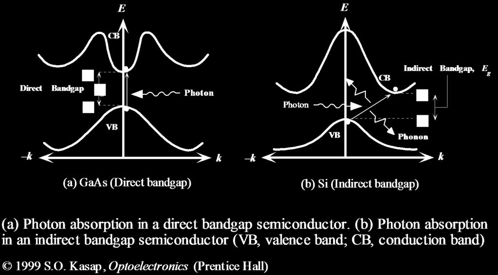
Valence band (VB) and conduction band (CB) of a semiconductor are separated by an energy gap E G = ev.
 and conduction band (CB) of a semiconductor are separated by an energy gap E G = ev.") 9.1 Direct ad idirect semicoductors Valece bad (VB) ad coductio bad (CB) of a semicoductor are searated by a eergy ga E G = 0.1... 4 ev. Direct semicoductor (e.g. GaAs): Miimum of the CB ad maximum of
9.1 Direct ad idirect semicoductors Valece bad (VB) ad coductio bad (CB) of a semicoductor are searated by a eergy ga E G = 0.1... 4 ev. Direct semicoductor (e.g. GaAs): Miimum of the CB ad maximum of
Monograph On Semi Conductor Diodes
 ISSN (ONLINE) : 395-695X ISSN (PRINT) : 395-695X Available olie at www.ijarbest.com Iteratioal Joural of Advaced Research i Biology, Ecology, Sciece ad Techology (IJARBEST) Vol. 1, Issue 3, Jue 015 Moograh
Bipolar Junction Transistors
 ipolar Juctio Trasistors ipolar juctio trasistor (JT) was iveted i 948 at ell Telephoe Laboratories Sice 97, the high desity ad low power advatage of the MOS techology steadily eroded the JT s early domiace.
Lecture 3. Electron and Hole Transport in Semiconductors
 Lecture 3 lectro ad Hole Trasort i Semicoductors I this lecture you will lear: How electros ad holes move i semicoductors Thermal motio of electros ad holes lectric curret via lectric curret via usio Semicoductor
Semiconductor Electronic Devices
 Semicoductor lectroic evices Course Codes: 3 (UG) 818 (PG) Lecturer: Professor thoy O eill mail: athoy.oeill@cl.ac.uk ddress: 4.31, Merz Court ims: To provide a specialist kowledge of semicoductor devices.
Forward and Reverse Biased Junctions
 TEMARIO DEL CURSO DE FUNDAMENTOS DE FÍSICA DE SEMICONDUCTORES 1. Itroducció a Física Electróica 1.1 Proiedades de cristales y crecimieto de semicoductores 1. Átomos y electroes 1.3 Badas de eergía y ortadores
Modeling and Simulation of Metal-Semiconductor-Metal Photodetector using VHDL-AMS
 Modelig ad Simulatio of Metal-Semicoductor-Metal Photodetector usig VHDL-AMS Shu Wu ad Sug-Mo Kag Deartmet of Electrical Egieerig, Uiversity of Califoria, Sata Cruz, Sata Cruz, CA 9564, USA wushu@soe.ucsc.edu
Bohr s Atomic Model Quantum Mechanical Model
 September 7, 0 - Summary - Itroductio to Atomic Theory Bohr s Atomic Model Quatum Mechaical Model 3- Some Defiitio 3- Projects Temperature Pressure Website Subject Areas Plasma is a Mixture of electros,
KJ 8056 CHAPTER 1. ELECTROCHEMICAL SENSORS. Part B. Semiconductor devices as chemical sensors
 NTNUet. of Chemistry KJ 8056 CHAPTER 1. ELECTROCHEMICAL SENSORS Part B. Semicoductor devices as chemical sesors CONTENTS By F. G. Baica, August 2006 B.1. Semicoductors devices a) Silico ad Germaium semicoductors
Lecture #25. Amplifier Types
 ecture #5 Midterm # formatio ate: Moday November 3 rd oics to be covered: caacitors ad iductors 1 st -order circuits (trasiet resose) semicoductor material roerties juctios & their alicatios MOSFEs; commo-source
The Bipolar Transistor
 hater 2 The Biolar Trasistor hater 2 The Biolar Trasistor Bardee, Brattai ad Shockley develoed the Biolar Juctio Trasistor i 1947 at Bell Laboratories [1]. These researchers oticed that i certai exerimetal
SOLUTIONS: ECE 606 Homework Week 7 Mark Lundstrom Purdue University (revised 3/27/13) e E i E T
 e E i E T") SOUIONS: ECE 606 Homework Week 7 Mark udstrom Purdue Uiversity (revised 3/27/13) 1) Cosider a - type semicoductor for which the oly states i the badgap are door levels (i.e. ( E = E D ). Begi with the
SOUIONS: ECE 606 Homework Week 7 Mark udstrom Purdue Uiversity (revised 3/27/13) 1) Cosider a - type semicoductor for which the oly states i the badgap are door levels (i.e. ( E = E D ). Begi with the
Phys 102 Lecture 25 The quantum mechanical model of light
 Phys 102 Lecture 25 The quatum mechaical model of light 1 Recall last time Problems with classical physics Stability of atoms Atomic spectra Photoelectric effect Quatum model of the atom Bohr model oly
Theoretical models and simulation of optoelectronic properties of a-si-h PIN photosensors
 Proceedigs of the 8th Iteratioal Coferece o Sesig Techology, Se. 2-4, 214, iverool, UK Theoretical models ad simulatio of otoelectroic roerties of a-si-h PIN hotosesors Wagah F. Mohammed 1, Muther N. Al-Tikriti
ECE 442. Spring, Lecture - 4
 ECE 44 Power Semicoductor Devices ad Itegrated circuits Srig, 6 Uiversity of Illiois at Chicago Lecture - 4 ecombiatio, geeratio, ad cotiuity equatio 1. Geeratio thermal, electrical, otical. ecombiatio
Lecture 6. Semiconductor physics IV. The Semiconductor in Equilibrium
 Lecture 6 Semicoductor physics IV The Semicoductor i Equilibrium Equilibrium, or thermal equilibrium No exteral forces such as voltages, electric fields. Magetic fields, or temperature gradiets are actig
Schottky diodes: I-V characteristics
 chottky diodes: - characteristics The geeral shape of the - curve i the M (-type) diode are very similar to that i the p + diode. However the domiat curret compoets are decidedly differet i the two diodes.
Two arbitrary semiconductors generally have different electron affinities, bandgaps, and effective DOSs. An arbitrary example is shown below.
 9. Heterojuctios Semicoductor heterojuctios A heterojuctio cosists of two differet materials i electrical equilibrium separated by a iterface. There are various reasos these are eeded for solar cells:
Lecture 3-7 Semiconductor Lasers.
 Laser LED Stimulated emissio Spotaeous emissio Laser I th I Typical output optical power vs. diode curret (I) characteristics ad the correspodig output spectrum of a laser diode.?1999 S.O. Kasap, Optoelectroics
Chapter 4. Photodetectors
 Chapter 4 Photodetectors Types of photodetectors: Photoconductos Photovoltaic Photodiodes Avalanche photodiodes (APDs) Resonant-cavity photodiodes MSM detectors In telecom we mainly use PINs and APDs.
ECEN Microelectronics. Semiconductor Physics and P/N junctions 2/05/19
 ECEN 3250 Microelectroics Semicoductor Physics ad P/N juctios 2/05/19 Professor J. Gopiath Professor J. Gopiath Uiversity of Colorado at Boulder Microelectroics Sprig 2014 Overview Eergy bads Atomic eergy
Lecture 9. NMOS Field Effect Transistor (NMOSFET or NFET)
") ecture 9 MOS Field ffect Trasistor (MOSFT or FT) this lecture you will lear: The oeratio ad workig of the MOS trasistor A MOS aacitor with a hael otact ( Si) metal cotact Si Si GB B versio layer PSi substrate
ecture 9 MOS Field ffect Trasistor (MOSFT or FT) this lecture you will lear: The oeratio ad workig of the MOS trasistor A MOS aacitor with a hael otact ( Si) metal cotact Si Si GB B versio layer PSi substrate
Summary of pn-junction (Lec )
") Lecture #12 OUTLNE Diode aalysis ad applicatios cotiued The MOFET The MOFET as a cotrolled resistor Pich-off ad curret saturatio Chael-legth modulatio Velocity saturatio i a short-chael MOFET Readig Howe
Lecture #12 OUTLNE Diode aalysis ad applicatios cotiued The MOFET The MOFET as a cotrolled resistor Pich-off ad curret saturatio Chael-legth modulatio Velocity saturatio i a short-chael MOFET Readig Howe
Mark Lundstrom Spring SOLUTIONS: ECE 305 Homework: Week 5. Mark Lundstrom Purdue University
 Mark udstrom Sprig 2015 SOUTIONS: ECE 305 Homework: Week 5 Mark udstrom Purdue Uiversity The followig problems cocer the Miority Carrier Diffusio Equatio (MCDE) for electros: Δ t = D Δ + G For all the
Lecture 9: Diffusion, Electrostatics review, and Capacitors. Context
 EECS 5 Sprig 4, Lecture 9 Lecture 9: Diffusio, Electrostatics review, ad Capacitors EECS 5 Sprig 4, Lecture 9 Cotext I the last lecture, we looked at the carriers i a eutral semicoductor, ad drift currets
Solid State Device Fundamentals
 Solid State Device Fudametals ENS 345 Lecture Course by Alexader M. Zaitsev alexader.zaitsev@csi.cuy.edu Tel: 718 982 2812 4N101b 1 Thermal motio of electros Average kietic eergy of electro or hole (thermal
Introduction to Solid State Physics
 Itroductio to Solid State Physics Class: Itegrated Photoic Devices Time: Fri. 8:00am ~ 11:00am. Classroom: 資電 206 Lecturer: Prof. 李明昌 (Mig-Chag Lee) Electros i A Atom Electros i A Atom Electros i Two atoms
Key Questions. ECE 340 Lecture 36 : MOSFET II 4/28/14
 Thigs you should kow whe you leae C 40 Lecture 6 : MOSFT Class Outlie: Short Chael ffects Key Questios Why is the mobility i the chael lower tha i the bulk? Why do strog electric fields degrade chael mobility?
Photodetectors Read: Kasip, Chapter 5 Yariv, Chapter 11 Class Handout. ECE 162C Lecture #13 Prof. John Bowers
 Photodetectors Read: Kasip, Chapter 5 Yariv, Chapter 11 Class Handout ECE 162C Lecture #13 Prof. John Bowers Definitions Quantum efficiency η: Ratio of the number of electrons collected to the number of
Exercises and Problems
 HW Chapter 4: Oe-Dimesioal Quatum Mechaics Coceptual Questios 4.. Five. 4.4.. is idepedet of. a b c mu ( E). a b m( ev 5 ev) c m(6 ev ev) Exercises ad Problems 4.. Model: Model the electro as a particle
Digital Integrated Circuits. Inverter. YuZhuo Fu. Digital IC. Introduction
 Digital Itegrated Circuits Iverter YuZhuo Fu Itroductio outlie CMOS at a glace CMOS static behavior CMOS dyamic behavior Power, Eergy, ad Eergy Delay Persective tech. /48 outlie CMOS at a glace CMOS static
Doped semiconductors: donor impurities
 Doped semicoductors: door impurities A silico lattice with a sigle impurity atom (Phosphorus, P) added. As compared to Si, the Phosphorus has oe extra valece electro which, after all bods are made, has
Experimental Fact: E = nhf
 CHAPTR 3 The xperimetal Basis of Quatum PHYS-3301 Lecture 4 Sep. 6, 2018 3.1 Discovery of the X Ray ad the lectro 3.2 Determiatio of lectro Charge 3.3 Lie Spectra 3.4 Quatizatio 3.5 Blackbody Radiatio
MODULE 1.2 CARRIER TRANSPORT PHENOMENA
 MODULE 1.2 CARRIER TRANSPORT PHENOMENA Carrier Trasort Pheoeo Carrier drift: obility, coductivity ad velocity saturatio Carrier Diffusio: diffusio curret desity, total curret desity The Eistei relatio
Complementi di Fisica Lectures 25-26
 Comlemeti di Fisica Lectures 25-26 Livio Laceri Uiversità di Trieste Trieste, 14/15-12-2015 i these lectures Itroductio No or quasi-equilibrium: excess carriers ijectio Processes for geeratio ad recombiatio
Regenerative Property
 DESIGN OF LOGIC FAMILIES Some desirable characteristics to have: 1. Low ower dissiatio. High oise margi (Equal high ad low margis) 3. High seed 4. Low area 5. Low outut resistace 6. High iut resistace
LEC E T C U T R U E R E 17 -Photodetectors
 LECTURE 17 -Photodetectors Topics to be covered Photodetectors PIN photodiode Avalanche Photodiode Photodetectors Principle of the p-n junction Photodiode A generic photodiode. Photodetectors Principle
Consider the circuit below. We have seen this one already. As before, assume that the BJT is on and in forward active operation.
 Saturatio Cosider the circuit below. We have see this oe already. As before, assume that the BJT is o ad i forward active operatio. VCC 0 V VBB ib RC 0 k! RB 3V 47 k! vbe ic vce βf 00. ( )( µ µ ). (. )(!!
ECE606: Solid State Devices Lecture 19 Bipolar Transistors Design
 606: Solid State Devices Lecture 9 ipolar Trasistors Desig Gerhard Klimeck gekco@purdue.edu Outlie ) urret gai i JTs ) osideratios for base dopig 3) osideratios for collector dopig 4) termediate Summary
YuZhuo Fu Office location:417 room WeiDianZi building,no 800 DongChuan road,minhang Campus
 Digital Itegrated Circuits YuZhuo Fu cotact:fuyuzhuo@ic.sjtu.edu.c Office locatio:417 room WeiDiaZi buildig,no 800 DogChua road,mihag Camus Itroductio Digital IC outlie CMOS at a glace CMOS static behavior
Digital Integrated Circuits
 Digital Itegrated Circuits YuZhuo Fu cotact:fuyuzhuo@ic.sjtu.edu.c Office locatio:417 room WeiDiaZi buildig,no 800 DogChua road,mihag Camus Itroductio outlie CMOS at a glace CMOS static behavior CMOS dyamic
1. pn junction under bias 2. I-Vcharacteristics
 Lecture 10 The p Juctio (II) 1 Cotets 1. p juctio uder bias 2. I-Vcharacteristics 2 Key questios Why does the p juctio diode exhibit curret rectificatio? Why does the juctio curret i forward bias icrease
Prototyping of III-N LEDs by Laser Direct Writing Techniques
 Prototyig of III-N LEDs by Laser Direct Writig Techiques Michael Kuzer, Rüdiger Moser, Christia Goßler, Klaus Köhler, Wilfried Pletsche, Ulrich T. Schwarz ad Joachim Wager Frauhofer-Istitut für Agewadte
Lecture 4: Heterojunction pn-diode
 Lecture 4: Heterojuctio -ioe 16-1-5 Lecture 4, High See Devices 16 1 Lecture 4: Heterojuctio P-ioe + heterojuctio uer equilibrium + heterojuctio uer exterl s Gre heterojuctios + gre heterojuctio: Curret
Basic Concepts of Electricity. n Force on positive charge is in direction of electric field, negative is opposite
 Basic Cocepts of Electricity oltage E Curret I Ohm s Law Resistace R E = I R 1 Electric Fields A electric field applies a force to a charge Force o positive charge is i directio of electric field, egative
Chapter 2 Motion and Recombination of Electrons and Holes
 Chapter 2 Motio ad Recombiatio of Electros ad Holes 2.1 Thermal Eergy ad Thermal Velocity Average electro or hole kietic eergy 3 2 kt 1 2 2 mv th v th 3kT m eff 3 23 1.38 10 JK 0.26 9.1 10 1 31 300 kg
ELECTRONICS AND COMMUNICATION ENGINEERING ESE TOPICWISE OBJECTIVE SOLVED PAPER-I
 ELECTRONICS AND COMMUNICATION ENGINEERING ESE TOPICWISE OBJECTIVE SOLVED PAPER-I From (1991 018) Office : F-16, (Lower Basemet), Katwaria Sarai, New Delhi-110016 Phoe : 011-65064 Mobile : 81309090, 9711853908
EECS130 Integrated Circuit Devices
 EECS130 Itegrated Circuit Devices Professor Ali Javey 9/04/2007 Semicoductor Fudametals Lecture 3 Readig: fiish chapter 2 ad begi chapter 3 Aoucemets HW 1 is due ext Tuesday, at the begiig of the class.
Solid State Device Fundamentals
 Solid State Device Fudametals ES 345 Lecture ourse by Alexader M. Zaitsev alexader.zaitsev@csi.cuy.edu Tel: 718 98 81 4101b ollege of State Islad / UY Dopig semicoductors Doped semicoductors are semicoductors,
Examination No. 3 - Tuesday, Nov. 15
 NAME (lease rit) SOLUTIONS ECE 35 - DEVICE ELECTRONICS Fall Semester 005 Examiati N 3 - Tuesday, Nv 5 3 4 5 The time fr examiati is hr 5 mi Studets are allwed t use 3 sheets f tes Please shw yur wrk, artial
ECE606: Solid State Devices Lecture 20. Heterojunction Bipolar Transistor
 C606: Solid State Devices Lecture 0 Heterojuctio ipolar Trasistor Gerhard Klimeck gekco@purdue.edu 1 Outlie 1. Itroductio. quilibrium solutio for heterojuctio 3. Types of heterojuctios 4. Itermediate Summary
Why? The atomic nucleus. Radioactivity. Nuclear radiations. The electrons and the nucleus. Length scale of the nature
 The atomic ucleus. Radioactivity. Nuclear radiatios László Smeller Why? Medical alicatios of the uclear radiatio: - Nuclear imagig - Radiotheray Legth scale of the ature m meter me -3 millimeter size of
Chapter 2 Motion and Recombination of Electrons and Holes
 Chapter 2 Motio ad Recombiatio of Electros ad Holes 2.1 Thermal Motio 3 1 2 Average electro or hole kietic eergy kt mv th 2 2 v th 3kT m eff 23 3 1.38 10 JK 0.26 9.1 10 1 31 300 kg K 5 7 2.310 m/s 2.310
Classification of DT signals
 Comlex exoetial A discrete time sigal may be comlex valued I digital commuicatios comlex sigals arise aturally A comlex sigal may be rereseted i two forms: jarg { z( ) } { } z ( ) = Re { z ( )} + jim {