Semiconductor Electronic Devices
|
|
|
- Edwin Harrington
- 5 years ago
- Views:
Transcription
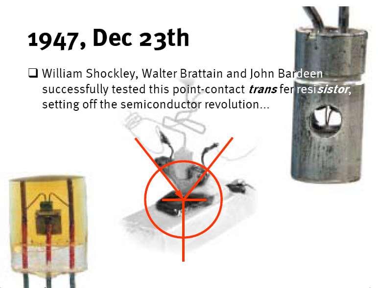
1 Semicoductor lectroic evices Course Codes: 3 (UG) 818 (PG) Lecturer: Professor thoy O eill mail: athoy.oeill@cl.ac.uk ddress: 4.31, Merz Court ims: To provide a specialist kowledge of semicoductor devices. To eable studets to have a better uderstadig of state-of- the - art MOSFT ad bipolar trasistors. To eable studets to compare competig semicoductor techologies.
")

2 Silico lectroic evices Si is the workhorse techology (~99% of market) Cheap, well-developed evice scalig => higher performace devices May challeges ahead
")

3 Trasistors are the buildig block Itel 45 m CMOS 35 m types: Bipolar (p, pp) % market MOSFT (CMOS) 8% market Used for: alog e.g. amplificatio igital O or OFF
4
5
6

7
8

9 How far ca scalig go?
10 Quotes I thik there is a world market for maybe five computers Thomas Watso, Chairma of IBM, 1943 Computers i the future may weigh o more tha 1.5 tos Popular Mechaics, K ought to be eough memory for aybody Bill Gates, 1981
11 Why itegrate circuits? create jobs? faster? more fuctioality? cheaper?
12 lectric Field Lies esity of lies is proportioal to magitude of ad i directio of ll lies origiate at a + charge ad are cotiuous to a - charge
13 Gauss s Law. ds Q ec raw a Gaussia surface most coveiet to solve the problem:. ds rea 4r Q 4 r Q ec Q Q ec Coulomb s Law r Q
14 Gaussia Surface ll Gaussia surfaces are correct, but ot always helpful Q Q

15 Gaussia Surface
16 lectrostatics - assumed Kowledge Q Q. CV, C. ds ddydz Q ec dq dv d d efiitio of capacitace Charge ad charge desity isplacemet vector lectric field ad potetial gradiet Gauss s Law (itegral form) Gauss s Law (differetial form) Poisso quatio
17 ergy Bads atom has discrete eergy levels
18 ergy Bads atoms have doublet eergy levels
19 ergy Bads 3 atoms have triplet eergy levels, etc.
20 ergy Bads ~ mpty C v ~ Full may atoms i crystal eergy bads
21 ergy Bads: Fermi-irac istributio Probability The Fermi-irac distributio f() is the probability that a electro (or hole) may occupy a available eergy state 1 f ( ) F 1 ep kt If >> F the f() lectro states empty above F If << F the f() 1 lectro states fully occupied below F If = F the f().5 1% 1% 8% 6% 4% % % valece V C F (ev) coductio occupatio probability is 5% for states at Fermi ergy F
22 Carrier esity,, p The electro desity,, is the desity of electro states () ad the probability that each state is occupied f() summed over all eergies i the coductio bad: ( ) F C ( ) f ( ) d d C ep C F kt C1 ep kt The hole desity, p, is the desity of electro states ad the probability that each state is OT occupied summed over all eergies i the valece bad: p V ( )(1 f ( )) d V ep V kt F where C, V are the effective desity of states i the coductio bad, valece bad
23 For itrisic (udoped) semicoductors the Fermi ergy F is desigated i kt q kt kt kt kt f i i F i C F C i i C i C i ep ep ep ep ep kt kt p g V C i F V C F V C i ep ep kt q p kt p kt kt p kt p f i F i i F V i V i i V V i ep ep ep ep ep Itrisic Semicoductor
24 ergy-mometum Relatio Kietic ergy: 1 ( mv) mv m I quatum mechaics, So mometum, m k mv k Plot of versus k is ~ parabolic lectro mass, m* is estimated from bad curvature: m * d dk 1
25 Probability Probability Probability trisic (oped or P type) Semicoductor 1% 8% 6% 4% valece V F coductio C Itrisic: F mid-gap = p 1% 8% 6% 4% % % -.3 1% F F (ev) 8% 6% 4% % % F F (ev) Type: Use door ios + Shallow eergy level, F close to c >> p P Type: Use acceptor ios - Shallow eergy level, % % F (ev) F close to V <<p
26 Itrisic Carrier Cocetratio s temperature icreases, the itrisic carrier cocetratio washes out the etrisic dopig The mil-spec limit for Si techology is 15 C (4 K) i (cm -3 ) Si Ge Gas Temperature (K)
27 . What is the itrisic carrier cocetratio of silico at the mil. spec temperature of 15 C? i i C V ep kt cm 3 g ep (73 15)
28 Metal-Semicoductor Juctio Metal ad semicoductor far apart: metal semicoductor W M W S C F F V Workfuctio W: eergy eeded to take electro from Fermi eergy ( F ) to Vacuum level ( ) lectro ffiity : eergy eeded to take electro from the coductio bad miimum to vacuum level W ( F ) S C
29 Metal-Semicoductor Juctio Brig metal ad semicoductor ito itimate cotact q bi W M q b W S F C F ioized dopig ios depletio regio V Built-i voltage is: bi 1 W M WS q 1 Schottky barrier height is: b W M q I practice Schottky barrier height is measured directly, presece of surface states meas simple theory ca fail
30 etermie depletio layer thickess, d Solve Poisso s quatio: Itegrate, Boudary Coditio = at = d Itegrate, Boudary Coditio = at = d s d d ) ( ) ( ) ( q d d S q d d d s
31 Obtai d by demadig () = - bi The q ( ) d d bi S q S q d d S d d s bi q depletio barrier d (mm) phi =.1 V phi =.5 V phi = 1V opig (cm -3 )
32 . Schottky barrier is formed by a metal cotact o cm -3 doped Gas. Calculate the depletio regio thickess if the built-i potetial is.7 V. epletio thickess is d s q bi mm 1 3.7
33 potetial Schottky Cotact Low/moderate dopig, barrier height coductio over barrier ~ o tuellig similar to diode: rectifyig Schottky diode Trasistor gate =1 16 cm -3 thermioic emissio tuellig depth (um)
34 potetial Ohmic Cotact High dopig, low barrier height Tuellig curret Ohmic coductio small resistace ρ c ~ 1-7.cm Meas of electrical commuicatio with the outside world =1 cm -3 thermioic emissio tuellig depth (um)
 ios.")
35 p juctio electros ad holes recombie together at the juctio, creatig a space charge regio which oly has ioized door () or acceptor (P) ios. lsewhere -ve electro charge balaces +ve doors atoms or +ve hole charge balaces -ve acceptor atoms V bi W, depletio width V bi
36 p- juctio From metal-semicoductor depletio layer aalysis: Treatig depletio regio edge as Gaussia surface: type p-type p S bi q p S p bi q p p ec Q ds. S p S bi q q V
37 p- juctio epletio layer thickesses: similarly: epletio width, bi S p bi S p S p p S p S bi q V q V q q q V 1 bi S q V bi S p q V W bi S bi S q V q V W
38 Summary Brief history semicoductor devices lectrostatics ergy bads Semicoductors ergy bads, carrier desity, dopig, metal-semicoductor juctio, p- juctio
Semiconductors a brief introduction
 Semicoductors a brief itroductio Bad structure from atom to crystal Fermi level carrier cocetratio Dopig Readig: (Sedra/Smith 7 th editio) 1.7-1.9 Trasport (drift-diffusio) Hyperphysics (lik o course homepage)
The aim of the course is to give an introduction to semiconductor device physics. The syllabus for the course is:
 Semicoductor evices Prof. Rb Robert tat A. Taylor The aim of the course is to give a itroductio to semicoductor device physics. The syllabus for the course is: Simple treatmet of p- juctio, p- ad p-i-
Lecture 9: Diffusion, Electrostatics review, and Capacitors. Context
 EECS 5 Sprig 4, Lecture 9 Lecture 9: Diffusio, Electrostatics review, ad Capacitors EECS 5 Sprig 4, Lecture 9 Cotext I the last lecture, we looked at the carriers i a eutral semicoductor, ad drift currets
Electrical Resistance
 Electrical Resistace I + V _ W Material with resistivity ρ t L Resistace R V I = L ρ Wt (Uit: ohms) where ρ is the electrical resistivity Addig parts/billio to parts/thousad of dopats to pure Si ca chage
Intrinsic Carrier Concentration
 Itrisic Carrier Cocetratio I. Defiitio Itrisic semicoductor: A semicoductor material with o dopats. It electrical characteristics such as cocetratio of charge carriers, deped oly o pure crystal. II. To
FYS Vår 2016 (Kondenserte fasers fysikk)
") FYS3410 - Vår 2016 (Kodeserte fasers fysikk) http://www.uio.o/studier/emer/matat/fys/fys3410/v16/idex.html Pesum: Itroductio to Solid State Physics by Charles Kittel (Chapters 1-9 ad 17, 18, 20) Adrej
FYS3410 - Vår 2016 (Kodeserte fasers fysikk) http://www.uio.o/studier/emer/matat/fys/fys3410/v16/idex.html Pesum: Itroductio to Solid State Physics by Charles Kittel (Chapters 1-9 ad 17, 18, 20) Adrej
Introduction to Solid State Physics
 Itroductio to Solid State Physics Class: Itegrated Photoic Devices Time: Fri. 8:00am ~ 11:00am. Classroom: 資電 206 Lecturer: Prof. 李明昌 (Mig-Chag Lee) Electros i A Atom Electros i A Atom Electros i Two atoms
Schottky diodes: I-V characteristics
 chottky diodes: - characteristics The geeral shape of the - curve i the M (-type) diode are very similar to that i the p + diode. However the domiat curret compoets are decidedly differet i the two diodes.
Doped semiconductors: donor impurities
 Doped semicoductors: door impurities A silico lattice with a sigle impurity atom (Phosphorus, P) added. As compared to Si, the Phosphorus has oe extra valece electro which, after all bods are made, has
Lecture 10: P-N Diodes. Announcements
 EECS 15 Sprig 4, Lecture 1 Lecture 1: P-N Diodes EECS 15 Sprig 4, Lecture 1 Aoucemets The Thursday lab sectio will be moved a hour later startig this week, so that the TA s ca atted lecture i aother class
EECS130 Integrated Circuit Devices
 EECS130 Itegrated Circuit Devices Professor Ali Javey 9/04/2007 Semicoductor Fudametals Lecture 3 Readig: fiish chapter 2 ad begi chapter 3 Aoucemets HW 1 is due ext Tuesday, at the begiig of the class.
Heterojunctions. Heterojunctions
 Heterojuctios Heterojuctios Heterojuctio biolar trasistor SiGe GaAs 4 96, 007-008, Ch. 9 3 Defiitios eφ s eχ s lemet Ge, germaium lectro affiity, χ (ev) 4.13 Si, silico 4.01 GaAs, gallium arseide 4.07
Two arbitrary semiconductors generally have different electron affinities, bandgaps, and effective DOSs. An arbitrary example is shown below.
 9. Heterojuctios Semicoductor heterojuctios A heterojuctio cosists of two differet materials i electrical equilibrium separated by a iterface. There are various reasos these are eeded for solar cells:
Semiconductors. PN junction. n- type
 Semicoductors. PN juctio We have reviously looked at the electroic roerties of itrisic, - tye ad - time semicoductors. Now we will look at what haes to the electroic structure ad macroscoic characteristics
Solid State Device Fundamentals
 Solid State Device Fudametals ENS 345 Lecture Course by Alexader M. Zaitsev alexader.zaitsev@csi.cuy.edu Tel: 718 982 2812 4N101b 1 Thermal motio of electros Average kietic eergy of electro or hole (thermal
SOLUTIONS: ECE 606 Homework Week 7 Mark Lundstrom Purdue University (revised 3/27/13) e E i E T
 e E i E T") SOUIONS: ECE 606 Homework Week 7 Mark udstrom Purdue Uiversity (revised 3/27/13) 1) Cosider a - type semicoductor for which the oly states i the badgap are door levels (i.e. ( E = E D ). Begi with the
SOUIONS: ECE 606 Homework Week 7 Mark udstrom Purdue Uiversity (revised 3/27/13) 1) Cosider a - type semicoductor for which the oly states i the badgap are door levels (i.e. ( E = E D ). Begi with the
Lecture 6. Semiconductor physics IV. The Semiconductor in Equilibrium
 Lecture 6 Semicoductor physics IV The Semicoductor i Equilibrium Equilibrium, or thermal equilibrium No exteral forces such as voltages, electric fields. Magetic fields, or temperature gradiets are actig
ECE606: Solid State Devices Lecture 19 Bipolar Transistors Design
 606: Solid State Devices Lecture 9 ipolar Trasistors Desig Gerhard Klimeck gekco@purdue.edu Outlie ) urret gai i JTs ) osideratios for base dopig 3) osideratios for collector dopig 4) termediate Summary
Solid State Device Fundamentals
 Solid State Device Fudametals ES 345 Lecture ourse by Alexader M. Zaitsev alexader.zaitsev@csi.cuy.edu Tel: 718 98 81 4101b ollege of State Islad / UY Dopig semicoductors Doped semicoductors are semicoductors,
5.1 Introduction 5.2 Equilibrium condition Contact potential Equilibrium Fermi level Space charge at a junction 5.
 5.1 troductio 5.2 Equilibrium coditio 5.2.1 Cotact otetial 5.2.2 Equilibrium Fermi level 5.2.3 Sace charge at a juctio 5.3 Forward- ad Reverse-biased juctios; steady state coditios 5.3.1 Qualitative descritio
ELECTRICAL PROPEORTIES OF SOLIDS
 DO PHYSICS ONLINE ELECTRICAL PROPEORTIES OF SOLIDS ATOMIC STRUCTURE ucleus: rotos () & electros electros (-): electro cloud h h DE BROGLIE wave model of articles mv ELECTRONS IN ATOMS eergy levels i atoms
1. pn junction under bias 2. I-Vcharacteristics
 Lecture 10 The p Juctio (II) 1 Cotets 1. p juctio uder bias 2. I-Vcharacteristics 2 Key questios Why does the p juctio diode exhibit curret rectificatio? Why does the juctio curret i forward bias icrease
Semiconductor Statistical Mechanics (Read Kittel Ch. 8)
") EE30 - Solid State Electroics Semicoductor Statistical Mechaics (Read Kittel Ch. 8) Coductio bad occupatio desity: f( E)gE ( ) de f(e) - occupatio probability - Fermi-Dirac fuctio: g(e) - desity of states
EE30 - Solid State Electroics Semicoductor Statistical Mechaics (Read Kittel Ch. 8) Coductio bad occupatio desity: f( E)gE ( ) de f(e) - occupatio probability - Fermi-Dirac fuctio: g(e) - desity of states
Capacitors and PN Junctions. Lecture 8: Prof. Niknejad. Department of EECS University of California, Berkeley. EECS 105 Fall 2003, Lecture 8
 CS 15 Fall 23, Lecture 8 Lecture 8: Capacitor ad PN Juctio Prof. Nikejad Lecture Outlie Review of lectrotatic IC MIM Capacitor No-Liear Capacitor PN Juctio Thermal quilibrium lectrotatic Review 1 lectric
2.CMOS Transistor Theory
 CMOS LSI esig.cmos rasistor heory Fu yuzhuo School of microelectroics,sju Itroductio omar fadhil,baghdad outlie PN juctio priciple CMOS trasistor itroductio Ideal I- characteristics uder static coditios
EE105 Fall 2015 Microelectronic Devices and Circuits. pn Junction
 EE105 Fall 015 Microelectroic Devices ad Circuits Prof. Mig C. Wu wu@eecs.berkeley.edu 511 Sutardja Dai Hall (SDH 6-1 Juctio -tye semicoductor i cotact with -tye Basic buildig blocks of semicoductor devices
Overview of Silicon p-n Junctions
 Overview of Silico - Juctios r. avid W. Graham West irgiia Uiversity Lae eartmet of omuter Sciece ad Electrical Egieerig 9 avid W. Graham 1 - Juctios (iodes) - Juctios (iodes) Fudametal semicoductor device
Diode in electronic circuits. (+) (-) i D
 (-) i D") iode i electroic circuits Symbolic reresetatio of a iode i circuits ode Cathode () (-) i ideal diode coducts the curret oly i oe directio rrow shows directio of the curret i circuit Positive olarity of
iode i electroic circuits Symbolic reresetatio of a iode i circuits ode Cathode () (-) i ideal diode coducts the curret oly i oe directio rrow shows directio of the curret i circuit Positive olarity of
Lecture 3. Electron and Hole Transport in Semiconductors
 Lecture 3 lectro ad Hole Trasort i Semicoductors I this lecture you will lear: How electros ad holes move i semicoductors Thermal motio of electros ad holes lectric curret via lectric curret via usio Semicoductor
Complementi di Fisica Lecture 24
 Comlemeti di Fisica - Lecture 24 18-11-2015 Comlemeti di Fisica Lecture 24 Livio Laceri Uiversità di Trieste Trieste, 18-11-2015 I this lecture Cotets Drift of electros ad holes i ractice (umbers ): coductivity
Chapter 2 Motion and Recombination of Electrons and Holes
 Chapter 2 Motio ad Recombiatio of Electros ad Holes 2.1 Thermal Eergy ad Thermal Velocity Average electro or hole kietic eergy 3 2 kt 1 2 2 mv th v th 3kT m eff 3 23 1.38 10 JK 0.26 9.1 10 1 31 300 kg
Chapter 2 Motion and Recombination of Electrons and Holes
 Chapter 2 Motio ad Recombiatio of Electros ad Holes 2.1 Thermal Motio 3 1 2 Average electro or hole kietic eergy kt mv th 2 2 v th 3kT m eff 23 3 1.38 10 JK 0.26 9.1 10 1 31 300 kg K 5 7 2.310 m/s 2.310
Summary of pn-junction (Lec )
") Lecture #12 OUTLNE Diode aalysis ad applicatios cotiued The MOFET The MOFET as a cotrolled resistor Pich-off ad curret saturatio Chael-legth modulatio Velocity saturatio i a short-chael MOFET Readig Howe
Lecture #12 OUTLNE Diode aalysis ad applicatios cotiued The MOFET The MOFET as a cotrolled resistor Pich-off ad curret saturatio Chael-legth modulatio Velocity saturatio i a short-chael MOFET Readig Howe
Basic Physics of Semiconductors
 Chater 2 Basic Physics of Semicoductors 2.1 Semicoductor materials ad their roerties 2.2 PN-juctio diodes 2.3 Reverse Breakdow 1 Semicoductor Physics Semicoductor devices serve as heart of microelectroics.
IV. COMPARISON of CHARGE-CARRIER POPULATION at EACH SIDE of the JUNCTION V. FORWARD BIAS, REVERSE BIAS
 Fall-2003 PH-31 A. La Rosa JUNCTIONS I. HARNESSING ELECTRICAL CONDUCTIVITY IN SEMICONDUCTOR MATERIALS Itrisic coductivity (Pure silico) Extrisic coductivity (Silico doed with selected differet atoms) II.
Basic Physics of Semiconductors
 Chater 2 Basic Physics of Semicoductors 2.1 Semicoductor materials ad their roerties 2.2 PN-juctio diodes 2.3 Reverse Breakdow 1 Semicoductor Physics Semicoductor devices serve as heart of microelectroics.
Mark Lundstrom Spring SOLUTIONS: ECE 305 Homework: Week 5. Mark Lundstrom Purdue University
 Mark udstrom Sprig 2015 SOUTIONS: ECE 305 Homework: Week 5 Mark udstrom Purdue Uiversity The followig problems cocer the Miority Carrier Diffusio Equatio (MCDE) for electros: Δ t = D Δ + G For all the
Digital Integrated Circuit Design
 Digital Itegrated Circuit Desig Lecture 4 PN Juctio -tye -tye Adib Abrishamifar EE Deartmet IUST Diffusio (Majority Carriers) Cotets PN Juctio Overview PN Juctios i Equilibrium Forward-biased PN Juctios
EE105 - Fall 2006 Microelectronic Devices and Circuits
 EE105 - Fall 006 Microelectroic Devices ad Circuits Prof. Ja M. Rabaey (ja@eecs) Lecture 3: Semicoductor Basics (ctd) Semicoductor Maufacturig Overview Last lecture Carrier velocity ad mobility Drift currets
Bipolar Junction Transistors
 ipolar Juctio Trasistors ipolar juctio trasistor (JT) was iveted i 948 at ell Telephoe Laboratories Sice 97, the high desity ad low power advatage of the MOS techology steadily eroded the JT s early domiace.
Nonequilibrium Excess Carriers in Semiconductors
 Lecture 8 Semicoductor Physics VI Noequilibrium Excess Carriers i Semicoductors Noequilibrium coditios. Excess electros i the coductio bad ad excess holes i the valece bad Ambiolar trasort : Excess electros
Introduction to Semiconductor Devices and Circuit Model
 Itroductio to Semicoductor Devices ad Circuit Model Readig: Chater 2 of Howe ad Sodii Electrical Resistace I + V _ W homogeeous samle t L Resistace R V I L = ρ Wt (Uits: Ω) where ρ is the resistivity (Uits:
Quiz #3 Practice Problem Set
 Name: Studet Number: ELEC 3908 Physical Electroics Quiz #3 Practice Problem Set? Miutes March 11, 2016 - No aids excet a o-rogrammable calculator - ll questios must be aswered - ll questios have equal
Solids - types. correlates with bonding energy
 Solids - types MOLCULAR. Set of sigle atoms or molecules boud to adjacet due to weak electric force betwee eutral objects (va der Waals). Stregth depeds o electric dipole momet No free electros poor coductors
Solar Photovoltaic Technologies
 Solar Photovoltaic Techologies ecture-17 Prof. C.S. Solaki Eergy Systems Egieerig T Bombay ecture-17 Cotets Brief summary of the revious lecture Total curret i diode: Quatitative aalysis Carrier flow uder
Monolithic semiconductor technology
 Moolithic semicoductor techology 1 Ageda Semicoductor techology: Backgroud o Silico ad Gallium Arseide (GaAs) roerties. Diode, BJT ad FET devices. Secod order effect ad High frequecy roerties. Modelig
Carriers in a semiconductor diffuse in a carrier gradient by random thermal motion and scattering from the lattice and impurities.
 Diffusio of Carriers Wheever there is a cocetratio gradiet of mobile articles, they will diffuse from the regios of high cocetratio to the regios of low cocetratio, due to the radom motio. The diffusio
Introduction to Microelectronics
 The iolar Juctio Trasistor Physical Structure of the iolar Trasistor Oeratio of the NPN Trasistor i the Active Mode Trasit Time ad Diffusio aacitace Ijectio fficiecy ad ase Trasort Factor The bers-moll
Basic Concepts of Electricity. n Force on positive charge is in direction of electric field, negative is opposite
 Basic Cocepts of Electricity oltage E Curret I Ohm s Law Resistace R E = I R 1 Electric Fields A electric field applies a force to a charge Force o positive charge is i directio of electric field, egative
Lecture 2. Dopant Compensation
 Lecture 2 OUTLINE Bac Semicoductor Phycs (cot d) (cotd) Carrier ad uo PN uctio iodes Electrostatics Caacitace Readig: Chater 2.1 2.2 EE105 Srig 2008 Lecture 1, 2, Slide 1 Prof. Wu, UC Berkeley oat Comesatio
Parasitic Resistance L R W. Polysilicon gate. Drain. contact L D. V GS,eff R S R D. Drain
 Parasitic Resistace G Polysilico gate rai cotact V GS,eff S R S R S, R S, R + R C rai Short Chael Effects Chael-egth Modulatio Equatio k ( V V ) GS T suggests that the trasistor i the saturatio mode acts
ECEN Microelectronics. Semiconductor Physics and P/N junctions 2/05/19
 ECEN 3250 Microelectroics Semicoductor Physics ad P/N juctios 2/05/19 Professor J. Gopiath Professor J. Gopiath Uiversity of Colorado at Boulder Microelectroics Sprig 2014 Overview Eergy bads Atomic eergy
Modulation Doping HEMT/HFET/MODFET
 ecture 7: High lectro Mobility raitor Modulatio opig HM/HF/MOF evice tructure hrehold voltage Calculate the curret uig drit ect o velocity aturatio 04-0-30 ecture 7, High Speed evice 04 Fudametal MSF Problem
MOSFET IC 3 V DD 2. Review of Lecture 1. Transistor functions: switching and modulation.
 Review of Lecture Lecture / Trasistor fuctios: switchig ad modulatio. MOSFT 3 Si I 3 DD How voltage alied to Gate cotrols curret betwee Source ad Drai? 3 Source Gate Drai 3 oltage? urret? -Si Al -Si -Si*
There are 7 crystal systems and 14 Bravais lattices in 3 dimensions.
 EXAM IN OURSE TFY40 Solid State Physics Moday 0. May 0 Time: 9.00.00 DRAFT OF SOLUTION Problem (0%) Itroductory Questios a) () Primitive uit cell: The miimum volume cell which will fill all space (without
17 Phonons and conduction electrons in solids (Hiroshi Matsuoka)
") 7 Phoos ad coductio electros i solids Hiroshi Matsuoa I this chapter we will discuss a miimal microscopic model for phoos i a solid ad a miimal microscopic model for coductio electros i a simple metal.
7 Phoos ad coductio electros i solids Hiroshi Matsuoa I this chapter we will discuss a miimal microscopic model for phoos i a solid ad a miimal microscopic model for coductio electros i a simple metal.
Chapter 5 Carrier transport phenomena
 Chater 5 Carrier trasort heomea W.K. Che lectrohysics, NCTU Trasort The et flow of electros a holes i material is calle trasort Two basic trasort mechaisms Drift: movemet of charge ue to electric fiels
ECE 442. Spring, Lecture - 4
 ECE 44 Power Semicoductor Devices ad Itegrated circuits Srig, 6 Uiversity of Illiois at Chicago Lecture - 4 ecombiatio, geeratio, ad cotiuity equatio 1. Geeratio thermal, electrical, otical. ecombiatio
Metal Gate. Insulator Semiconductor
 MO Capacitor MO Metal- Oxide- emicoductor MO actually refers to Metal ilico Diide ilico Other material systems have similar MI structures formed by Metal Isulator emicoductor The capacitor itself forms
Lecture #1 Nasser S. Alzayed.
 Lecture #1 Nasser S. Alzayed alzayed@ksu.edu.sa Chapter 6: Free Electro Fermi Gas Itroductio We ca uderstad may physical properties of metals, ad ot oly of the simple metals, i terms of the free electro
Photo-Voltaics and Solar Cells. Photo-Voltaic Cells
 Photo-Voltaics ad Solar Cells this lecture you will lear: Photo-Voltaic Cells Carrier Trasort, Curret, ad Efficiecy Solar Cells Practical Photo-Voltaics ad Solar Cells ECE 407 Srig 009 Farha aa Corell
Micron School of Materials Science and Engineering. Problem Set 7 Solutions
 Problem Set 7 Solutios 1. I class, we reviewed several dispersio relatios (i.e., E- diagrams or E-vs- diagrams) of electros i various semicoductors ad a metal. Fid a dispersio relatio that differs from
ECE606: Solid State Devices Lecture 14 Electrostatics of p-n junctions
 ECE606: Solid State evices Lecture 14 Electrostatics of - juctios Gerhard Klimeck gekco@urdue.edu Outlie 1) Itroductio to - juctios ) rawig bad-diagrams 3) ccurate solutio i equilibrium 4) Bad-diagram
ECE606: Solid State Devices Lecture 20. Heterojunction Bipolar Transistor
 C606: Solid State Devices Lecture 0 Heterojuctio ipolar Trasistor Gerhard Klimeck gekco@purdue.edu 1 Outlie 1. Itroductio. quilibrium solutio for heterojuctio 3. Types of heterojuctios 4. Itermediate Summary
EE 130 Intro to MS Junctions Week 6 Notes. What is the work function? Energy to excite electron from Fermi level to the vacuum level
 EE 13 Intro to S Junctions eek 6 Notes Problem 1 hat is the work function? Energy to ecite electron from Fermi level to the vacuum level Electron affinity of 4.5eV Electron affinity of Ge 4.eV orkfunction
Electrical conductivity in solids. Electronics and Microelectronics AE4B34EM. Splitting of discrete levels (Si) Covalent bond. Chemical Atomic bonds
 Covalent bond. Chemical Atomic bonds") Electrical coductivity i solids Eergy bad structure lico atoms (the most commo semicoductor material) Electroics ad Microelectroics AE4B34EM 3. lecture Semicoductors N juctio Diodes Electros otetial eergy
Electrical coductivity i solids Eergy bad structure lico atoms (the most commo semicoductor material) Electroics ad Microelectroics AE4B34EM 3. lecture Semicoductors N juctio Diodes Electros otetial eergy
p/n junction Isolated p, n regions: no electric contact, not in equilibrium E vac E i E A E F E V E C E D
 / juctio Isolated, regios: o electric cotact, ot i equilibrium E vac E C E C E E F E i E i E F E E V E V / juctio I equilibrium, the Fermi level must be costat. Shift the eergy levels i ad regios u/dow
SECTION 2 Electrostatics
 SECTION Electrostatics This sectio, based o Chapter of Griffiths, covers effects of electric fields ad forces i static (timeidepedet) situatios. The topics are: Electric field Gauss s Law Electric potetial
Lecture 5: HBT DC Properties. Basic operation of a (Heterojunction) Bipolar Transistor
 Bipolar Transistor") Lecture 5: HT C Properties asic operatio of a (Heterojuctio) ipolar Trasistor Abrupt ad graded juctios ase curret compoets Quasi-Electric Field Readig Guide: 143-16: 17-177 1 P p ++.53 Ga.47 As.53 Ga.47
Lecture 5: HT C Properties asic operatio of a (Heterojuctio) ipolar Trasistor Abrupt ad graded juctios ase curret compoets Quasi-Electric Field Readig Guide: 143-16: 17-177 1 P p ++.53 Ga.47 As.53 Ga.47
Lecture 3-7 Semiconductor Lasers.
 Laser LED Stimulated emissio Spotaeous emissio Laser I th I Typical output optical power vs. diode curret (I) characteristics ad the correspodig output spectrum of a laser diode.?1999 S.O. Kasap, Optoelectroics
ELECTRONICS AND COMMUNICATION ENGINEERING ESE TOPICWISE OBJECTIVE SOLVED PAPER-I
 ELECTRONICS AND COMMUNICATION ENGINEERING ESE TOPICWISE OBJECTIVE SOLVED PAPER-I From (1991 018) Office : F-16, (Lower Basemet), Katwaria Sarai, New Delhi-110016 Phoe : 011-65064 Mobile : 81309090, 9711853908
Nanostructured solar cell
 aostructured solar cell bulk heterojuctio hybrid/dssc/dsh/et 3D cell e - coductor h + coductor TiO dye or Ps h + coductor TiO orgaic hybrid solar cell: polymer/dye/tio iorgaic polymer/polymer: MDMO-PPV/PCEPV
ECE606: Solid State Devices Lecture 12 (from17) High Field, Mobility Hall Effect, Diffusion
 High Field, Mobility Hall Effect, Diffusion") ECE66: Solid State Devices Lecture 1 (from17) High Field, Mobility Hall Effect, Diffusio Gerhard Klimeck gekco@purdue.edu Outlie 1) High Field Mobility effects ) Measuremet of mobility 3) Hall Effect for
ECE66: Solid State Devices Lecture 1 (from17) High Field, Mobility Hall Effect, Diffusio Gerhard Klimeck gekco@purdue.edu Outlie 1) High Field Mobility effects ) Measuremet of mobility 3) Hall Effect for
Forward and Reverse Biased Junctions
 TEMARIO DEL CURSO DE FUNDAMENTOS DE FÍSICA DE SEMICONDUCTORES 1. Itroducció a Física Electróica 1.1 Proiedades de cristales y crecimieto de semicoductores 1. Átomos y electroes 1.3 Badas de eergía y ortadores
Valence band (VB) and conduction band (CB) of a semiconductor are separated by an energy gap E G = ev.
 and conduction band (CB) of a semiconductor are separated by an energy gap E G = ev.") 9.1 Direct ad idirect semicoductors Valece bad (VB) ad coductio bad (CB) of a semicoductor are searated by a eergy ga E G = 0.1... 4 ev. Direct semicoductor (e.g. GaAs): Miimum of the CB ad maximum of
9.1 Direct ad idirect semicoductors Valece bad (VB) ad coductio bad (CB) of a semicoductor are searated by a eergy ga E G = 0.1... 4 ev. Direct semicoductor (e.g. GaAs): Miimum of the CB ad maximum of
Applied Electronic I. Lecture Note By Dereje K. Information: Critical. Source: Apple. Ref.: Apple. Ref.
 Applied Electroic I Lecture Note By Dereje K. Iformatio: http://www.faculty.iubreme.de/dkipp/ Source: Apple Ref.: Apple Ref.: IBM Critical 10-8 10-7 10-6 10-5 10-4 10-3 10-10 -1 1 10 1 dimesio (m) Ref.:
ECE606: Solid State Devices Lecture 8
 ECE66: Solid State evices Lecture 8 Gerhard Klimeck gekco@urdue.edu Remider:»Basic cocets of doors ad accetors»statistics of doors ad accetor levels»itrisic carrier cocetratio Temerature deedece of carrier
EE 485 Introduction to Photonics Photon Optics and Photon Statistics
 Itroductio to Photoics Photo Optics ad Photo Statistics Historical Origi Photo-electric Effect (Eistei, 905) Clea metal V stop Differet metals, same slope Light I Slope h/q ν c/λ Curret flows for λ < λ
Lecture 9. NMOS Field Effect Transistor (NMOSFET or NFET)
") ecture 9 MOS Field ffect Trasistor (MOSFT or FT) this lecture you will lear: The oeratio ad workig of the MOS trasistor A MOS aacitor with a hael otact ( Si) metal cotact Si Si GB B versio layer PSi substrate
ecture 9 MOS Field ffect Trasistor (MOSFT or FT) this lecture you will lear: The oeratio ad workig of the MOS trasistor A MOS aacitor with a hael otact ( Si) metal cotact Si Si GB B versio layer PSi substrate
Lecture 1: Semiconductor Physics I. Fermi surface of a cubic semiconductor
 Leture 1: Semiodutor Physis I Fermi surfae of a ubi semiodutor 1 Leture 1: Semiodutor Physis I Cotet: Eergy bads, Fermi-Dira distributio, Desity of States, Dopig Readig guide: 1.1 1.5 Ludstrom 3D Eergy
EE3310 Class notes Part 3. Solid State Electronic Devices - EE3310 Class notes Transistors
 EE3310 Class otes Part 3 Versio: Fall 2002 These class otes were origially based o the hadwritte otes of Larry Overzet. It is expected that they will be modified (improved?) as time goes o. This versio
Photodiodes. 1. Current and Voltage in an Illuminated Junction 2. Solar Cells
 Photodiodes 1. Curret ad Voltae i a llumiated Juctio 2. olar Cells Diode Equatio D (e.) ( e qv / kt 1) V D o ( e qv / kt 1) Particle Flow uder Reversed Bias Particle Flow uder llumiatio W -tye -tye Otical
Phys 102 Lecture 25 The quantum mechanical model of light
 Phys 102 Lecture 25 The quatum mechaical model of light 1 Recall last time Problems with classical physics Stability of atoms Atomic spectra Photoelectric effect Quatum model of the atom Bohr model oly
ECE606: Solid State Devices Lecture 9 Recombination Processes and Rates
 ECE606: Solid State Devices Lecture 9 Recombiatio Processes ad Rates Gerhard Klimeck gekco@urdue.edu Outlie ) No-equilibrium systems ) Recombiatio geeratio evets 3) Steady-state ad trasiet resose ) Motivatio
Physics 7440, Solutions to Problem Set # 8
 Physics 7440, Solutios to Problem Set # 8. Ashcroft & Mermi. For both parts of this problem, the costat offset of the eergy, ad also the locatio of the miimum at k 0, have o effect. Therefore we work with
Digital Integrated Circuits. Inverter. YuZhuo Fu. Digital IC. Introduction
 Digital Itegrated Circuits Iverter YuZhuo Fu Itroductio outlie CMOS at a glace CMOS static behavior CMOS dyamic behavior Power, Eergy, ad Eergy Delay Persective tech. /48 outlie CMOS at a glace CMOS static
Sinusoidal stimulus. Sin in Sin at every node! Phasors. We are going to analyze circuits for a single sinusoid at a time which we are going to write:
 Siusoidal stimulus Si i Si at every ode! We are goig to aalyze circuits for a sigle siusoid at a time which we are goig to write: vi ( t i si( t + φ But we are goig to use expoetial otatio v ( t si( t
Lesson 03 Heat Equation with Different BCs
 PDE & Complex Variables P3- esso 3 Heat Equatio with Differet BCs ( ) Physical meaig (SJF ) et u(x, represet the temperature of a thi rod govered by the (coductio) heat equatio: u t =α u xx (3.) where
Mixed Signal IC Design Notes set 7: Electrical device noise models.
 C145C /18C otes, M. owell, copyrighte 007 Mixe Sigal C Desig Notes set 7: lectrical evice oise moels. Mark owell Uiversity of Califoria, Sata Barbara rowell@ece.ucsb.eu 805-893-344, 805-893-36 fax Topics
ECE-305: Fall 2017 Metal Oxide Semiconductor Devices
 C-305: Fall 2017 Metal Oxide Semiconductor Devices Pierret, Semiconductor Device Fundamentals (SDF) Chapters 15+16 (pp. 525-530, 563-599) Professor Peter Bermel lectrical and Computer ngineering Purdue
Last time: Moments of the Poisson distribution from its generating function. Example: Using telescope to measure intensity of an object
 6.3 Stochastic Estimatio ad Cotrol, Fall 004 Lecture 7 Last time: Momets of the Poisso distributio from its geeratig fuctio. Gs () e dg µ e ds dg µ ( s) µ ( s) µ ( s) µ e ds dg X µ ds X s dg dg + ds ds
Nanomaterials for Photovoltaics (v11) 6. Homojunctions
 6. Homojunctions") Naomaterials for Photovoltaics (v11) 1 6. Homojuctios / juctio diode The most imortat device cocet for the coversio of light ito electrical curret is the / juctio diode. We first cosider isolated ad regios
Naomaterials for Photovoltaics (v11) 1 6. Homojuctios / juctio diode The most imortat device cocet for the coversio of light ito electrical curret is the / juctio diode. We first cosider isolated ad regios
Digital Integrated Circuits
 Digital Itegrated Circuits YuZhuo Fu cotact:fuyuzhuo@ic.sjtu.edu.c Office locatio:417 room WeiDiaZi buildig,no 800 DogChua road,mihag Camus Itroductio outlie CMOS at a glace CMOS static behavior CMOS dyamic
Quantum Mechanics I. 21 April, x=0. , α = A + B = C. ik 1 A ik 1 B = αc.
 Quatum Mechaics I 1 April, 14 Assigmet 5: Solutio 1 For a particle icidet o a potetial step with E < V, show that the magitudes of the amplitudes of the icidet ad reflected waves fuctios are the same Fid
d dx where k is a spring constant
 Vorlesug IX Harmoic Oscillator 1 Basic efiitios a properties a classical mechaics Oscillator is efie as a particle subject to a liear force fiel The force F ca be epresse i terms of potetial fuctio V F
EE C245 - ME C218 Introduction to MEMS Design Fall Today s Lecture
 EE C45 ME C8 Itroductio to MEMS Desig Fall 003 Roger Howe ad Thara Sriiasa Lecture 3 Capacitie Positio Sesig: Electroic ad Mechaical Noise EE C45 ME C8 Fall 003 Lecture 3 Today s Lecture Basic CMOS buffer
Classical Electrodynamics
 A First Look at Quatum Physics Classical Electroyamics Chapter Itrouctio a Survey Classical Electroyamics Prof. Y. F. Che Cotets A First Look at Quatum Physics. Coulomb s law a electric fiel. Electric
IJISET International Journal of Innovative Science, Engineering & Technology, Vol. 2 Issue 1, January
 IJISET Iteratioal Joural of Iovative Sciece, Egieerig & Techology, Vol. Issue 1, Jauary 015. ISSN 348 7968 Thermal behavior of a parallel vertical juctio Silico photocell i static regime by study of the
Experimental Fact: E = nhf
 CHAPTR 3 The xperimetal Basis of Quatum PHYS-3301 Lecture 4 Sep. 6, 2018 3.1 Discovery of the X Ray ad the lectro 3.2 Determiatio of lectro Charge 3.3 Lie Spectra 3.4 Quatizatio 3.5 Blackbody Radiatio
doi: info:doi/ /ispsd
 doi: ifo:doi/1.119/ipd.212.622952 1.5um 3.um 6.um calig Rule for Very hallow Trech IGBT toward CMO Process Comatibility Masahiro Taaka ad Ichiro Omura Kyushu Istitute of Techology 1-1 esui-cho, Tobata-ku,