Micro Bolometer Dr. Lynn Fuller, Jackson Anderson
|
|
|
- Paula Lewis
- 6 years ago
- Views:
Transcription
1 ROCHESTER INSTITUTE OF TECHNOLOGY MICROELECTRONIC ENGINEERING Micro Bolometer Dr. Lynn Fuller, Jackson Anderson Webpage: Electrical and 82 Lomb Memorial Drive Rochester, NY Tel (585) Department webpage: MicroBolometer.ppt Page 1
2 ADOBE PRESENTER This PowerPoint module has been published using Adobe Presenter. Please click on the Notes tab in the left panel to read the instructors comments for each slide. Manually advance the slide by clicking on the play arrow or pressing the page down key. Page 2

3 OUTLINE Introduction Manufactures & Applications Theory Black Body Radiation Adsorption vs Wavelength Resistors Readout Amplifier Pixel Array Fabrication Process Test Results Packaging Commercial Devices Applications References Homework Page 3
4 INTRODUCTION A Bolometer is an infrared detector that works on a change in resistance resulting from the absorption of radiant infrared energy with wavelengths between 5 and 15µm. These sensors operate at room temperature and do not require cooling. At these wavelengths electron-hole pair generation is not the mechanism for resistance change since the photon energy is not higher than the material band gap. The infrared photons can be absorbed by the free carriers (electrons or holes) increasing their energy which upon relaxation increases the temperature of the material slightly. The sensor should be low mass, able to absorb infrared energy and be thermally isolated from surrounding materials. Materials such as amorphous silicon and vanadium oxide have been used for the sensor material. The resistors themselves should have a large temperature coefficient of resistance (TCR) and low sheet resistance (for low noise). Page 4


5 INTRODUCTION Page 5
6 CAMERA BUSINESS From Yole Development Page 6

7 MANUFACTURERS Agilent Fluke Corporation BAE Systems Raytheon L-3 Communications Infrared Products DRS Technologies GUIDR FLIR Systems Opgal Optronics Ltd Vumii Imaging InfraredVision Technology Corp. NEC Institut National d Optique Honeywell ULIS-IR Page 7
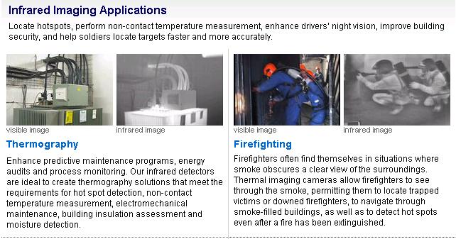
8 APPLICATIONS Page 8

9 DIGIKEY Page 9

10 IR CAMERA FOR THE SMARTPHONE From Yole Development Page 10

11 AGILENT U5855A TRUE IR THERMAL IMAGER Features Power adapter and cord Li-ion rechargeable battery SD memory card USB Standard-A to mini type-b interface cable Laser pointer and LED illuminator Both IR and visual images captured Zoom and fine focus Page 11


12 HOT PLATES IN SMFL Page 12
13 THEORY IR wavelength Resistance Change (Responsivity, TCR) Materials Noise Active vs Passive Page 13
14 BLACK BODY RADIATION From: Micromachined Transducers, Gregory T.A. Kovacs From: Solar Cells, Martin A. Green, Prentice Hall lpeak = 2898 µm / T Wien s Displacement Law lpeak = 2898/T (µm) h = E-34 J s = E-15 ev s l= c/n k=1.38e-23 J/K W l = radiant flux e(l) = emissivity (dimensionless, e=1 for black body) Page 14
15 PLANCK S LAW Planck s Law: (Spectral Radiance) Power per unit time radiated per unit area of emitting surface in the normal direction per unit solid angle per unit frequency. This equation is used to approximate emissions from black body sources. I is spectral radiance (w/m2/.) W l is radiant flux (w/m2) h = E-34 J s = E-15 ev s l= wavelength = c/n n = frequency c = 2.998E8 m/s k =1.38e-23 J/K e(l) = emissivity (dimensionless, e=1 for black body) Page 15
16 Adsorption Coefficient, a (1/cm) ABSORPTION VERSUS DISTANCE V I 1.00E+06 Absorption Coefficient vs Wavelength For Silicon n p I 1.00E E E E E E E-01 + V - I No Light More Light Most Light V 1.00E E E E E Wavelength (nm) f(x) = f(0) exp -a x Find % absorbed for Green light at x=5 µm and Red light at 5 µm Page 16


17 SILICON IS TRANSPARENT TO INFRARED Visible Picture Infrared Picture Note: eyeglass temperature is 25.6 C, face is ~30 C, and neck is ~35 C Page 17
18 ABSORPTION FOR POLYSILICON pg 210 Figure 7 by Timans et al. "Rapid Thermal Processing," in "Handbook of Semiconductor Manufacturing Technology," Nishi and Doering ed. Copyright Indicates free carrier absorption, higher doping gives higher absorption. At 1E19 cm-3 doping the absorption coefficient is ~5E3/cm much higher than single crystal silicon absorption shown above. (still looking for better absorption data) Page 18
19 EXAMPLE CALCULATIONS Calculate the response for a micro bolometer pixel (single resistor) to IR radiation from a black body emitter. Assumptions: IR Source Temperature = 300 C =573 K IR Source Physical Dimensions 8 x8 square plate, Emissivity = 1 Distance to the detector 10cm = 0.1m Detector Physical Dimensions and Properties N+ Polysilicon, Thickness 1.7um Doping 1E16cm-3, rhos=50 ohms/sq 100um x 100um pixel area Suspension in air, gap of 2um Suspension poly silicon 1.7um x 400um x 40um with aluminum 0.7um x 400um x 20um Page 19
20 EXAMPLE CALCULATIONS Assumptions: Assume Detector Absorption Coefficient is 5e3/cm constant for all wavelengths (1.3um to 10um) Si Window over detector (to block visible light) 55% transmission in IR from 1.3um to 10um Constants: Plank s Constant h=6.63e-34 J/s Boltzmann's Constant k=1.38e-23 J/K Speed of light c=2.998e8 m/s Thermal Conductivity (w/cmk) Si = um Al = 2.36 Air = SiO2 = Si3N4 = Layout Page 20
21 CALCULATION OF THERMAL RESISTANCE Calculation of thermal resistance between detector and ambient. Three parallel paths, through air, through poly suspension, through aluminum on suspension. Rth = (1/Cth) L/Area Air: Poly: Al: Cth= w/cmk, L=2um, Area=100um x 100um Rth air = 7692 K/w Cth=1.5 w/cmk, L=400um, Area=1.7um x 40um Rth poly = K/w Cth=2.36 w/cmk, L=400um, Area=0.7um x 20um Rth al = K/w Rth total = ~7000 K/w mostly the air gap Page 21
22 CALCULATION OF POWER FROM THE SOURCE Calculation of the power emitted from the source. The Power radiated from the source is equal to the Integral (sum) of the Spectral Radiance over the IR spectrum (1.3um to 10um) at the given source temperature. Planck s Law: (Spectral Radiance) Power per unit time radiated per unit area of emitting surface in the normal direction per unit solid angle per unit frequency. This is for a hemispherical emission source. Page 22
 of the emission versus wavelength, the area under the curve.")


23 Spectral Radiance (W/(m^2*Hz*steradian)) CALCULATION OF POWER REACHING THE DETECTOR The power reaching the detector is the integral (sum) of the emission versus wavelength, the area under the curve. If a silicon filter is used to block visible light we also multiply by the % transmission versus wavelength. The distance between the source and the detector and the area of the detector determine the solid angle in steradians. 4.00E E E E E E-11 Emission of a Blackbody at Given Temperature At Bolometer At Bolometer, with Si lens Any area on a sphere which is equal in area to the square of its radius, when observed from its center, subtends precisely one steradian. 1.00E E E l= wavelength = c/n n = frequency c = 2.998E8 m/s Wavelength (um) Page 23
24 CALCULATION OF POWER ABSORBED BY DETECTOR Solid angle = area of detector/distance 2 = 100um x 100um / 0.01m 2 = 1e-8 /.01 = 1E-6 Transmission through crystalline silicon filter = 55% Frequency = speed of light/wavelength After Filter Power = ~ 2E-11 x 1E-6 x 3E8/5um = watt/m2 Using the absorption coefficient of a =5E3/cm and thickness x=1.7um % absorption = 1- exp ( a x) = 57% Total Power absorbed by the detector Power total = x 57% = 6.84E-4 watts Page 24
25 CALCULATION OF RESISTANCE Total Power absorbed by the detector Power total = x 57% = 6.84E-4 watts Change in temperature = Power total x Thermal Resistance = 6.8e-4 w x 7000 K/w = K Resistance at 25 C, R = Rhos L/W + modifications for poly See Dr. Fullers Resistance Calculator R@300 K = ohms Resistance at elevated temperature C R@ K = ohms Page 25


26 CALCULATION OF RESISTANCE See Dr. Fullers Resistance Calculator K = ohms R@ K = ohms TCR Microelectronic = Engineering DR/DT =0.04 ohm/4.79 K = 0.835% Page 26
27 CIRCUIT CALCULATIONS V -V R This output voltage can be easily amplified Vout = 3 x -1.5 = mv R2 I = 3 / = 13.7 ma Power = I 2 R = (13.7mA) = mw Compared to signal power of mw This power is too large. A different circuit approach is needed. Page 27

28 CIRCUIT LTSPICE SIMULATION Page 28
29 CIRCUIT LTSPICE SIMULATION Vout 4.236mV Difference giving sensitivity = 14.1 uv/ K Power in Rsensor mw Compared to signal power of mw Page 29

30 Substrate set at 298 K SOLID WORKS SIMULATION Page 30

31 SUSPENDED POLYSILICON RESISTOR Page 31
32 SUSPENDED POLYSILICON RESISTOR Resistor No Heat Heat (No Light) Heat (Uncovered) Resistance Ω Ω Ω Page 32


33 SUSPENDED POLYSILICON RESISTOR Sensitivity = 10mohms/267ohms/100/ C = 0.004%/ C Compared to industry TCR s of 2.0%/ C Page 33
34 PIXEL LAYOUT Row Select V+ Column Vout Page 34
35 Column Out SINGLE PIXEL AND READOUT AMPLIFIER V+ Row Select Rs Pixel Readout Amp Vref - + Rref R1 + - R2 Analog Vout Page 35
36 Row Address Row Decoder Micro Bolometer 4x4 PIXEL ARRAY Column Address Column Amps & Analog Mux Serial Output Page 36

37 RESISTOR - BOLOMETER Page 37

38 RESISTOR 2 - BOLOMETER Page 38

39 RESISTOR 1 - BOLOMETER Page 39

40 RESISTOR 3 - BOLOMETER Page 40


41 Layout 12/23/2016 Jackson Anderson - Page 41 41

42 RESISTOR 2 641Ω Page 42

43 PICTURE OF PHOTOMASKS Page 43

44 DARK FIELD RETICLE FOR ASML Anchor, Non-Chrome Side Page 44

 2 = > 1.0 µm for NA = 0.")
45 ASML 5500/200 NA = 0.48 to 0.60 variable = 0.35 to 0.85 variable With Variable Kohler, or Variable Annular illumination Resolution = K1 l/na = ~ 0.35µm for NA=0.6, =0.85 Depth of Focus = k 2 l/(na) 2 = > 1.0 µm for NA = 0.6 i-line Stepper l = 365 nm 22 x 27 mm Field Size Page 45
46 STEPPER JOB Mask Barcode: Stepper Jobname: MCEE770-MEMS Level 0 (combi reticle) Level Clearout (combi reticle) Level SacOx Level Poly 1 Level Anchor Level Poly 2 Level CC Level Metal Level No Implant Level Release Page 46
47 SURFACE MEMS 2016 PROCESS 1. Starting wafer 2. PH03 level 0, Marks 3. ET29 Zero Etch 4. ID01-Scribe Wafer ID, D1 5. ET07 Resist Strip, Recipe FF 6. CL01 RCA clean 7. OX Å Oxide Tube 1 8. CV01 LPCVD Poly 5000Å 9. IM01 Implant P31, 2E16, 60KeV 10. PH03 level 1 Poly ET08 Poly Etch 12. ET07 Resist Strip, Recipe FF 13. CL01- RCA Clean 14. OX05 700Å Dry Oxide 15. CV02- LPCVD Nitride 4000Å 16. PH03 level 2 Anchor 17. ET29 Etch Nitride 18. ET07 - Resist Strip, Recipe FF 19. CL01 RCA Clean 20. CV03-TEOS SacOx Dep 1.75um 21. PH03 level 3 SacOx Define 22. ET06 - wet etch SacOx Define Etch 23. ET07- Resist Strip, Recipe FF 24. CL01 RCA Clean 25. CV01-LPCVD Poly 2um, 140 min 26. PH03 - level 4 No Implant 27. IM01-P31 2E16 100KeV 28. ET07 Resist Strip, Recipe FF 29. CL01 RCA Clean 30. OX05-500Å pad oxide 31. CV Å nitride 32. PH03 - level 5 Poly2 33. ET29 Plasma Etch Nitride 34. ET06 Wet Etch pad oxide 35. ET68 - STS Etch Poly2 36. ET07 - Resist Strip, Recipe FF 37. PH03 level 6 Contact Cut 38. ET29 Etch Nitride Contact Cut 39. ET06 Etch Oxide Contact Cut 40. ET07 Resist Strip, Recipe FF 41. CL01 RCA Clean two HF 42. ME01 Metal Deposition - Al 43. PH03 level 7 Metal 44. ET55 Metal Etch - wet 45. ET07 Resist Strip 46. PH03 level 8 Release 47. SA01 Saw wafers ½ Thru 48. Special Soap Clean 49. ET66 Final SacOx Etch 50. ET07 - Resist Strip with Acetone 51. Rinse and Dry w Isopropyl Pull 52. TE01 wafer level testing 53. SEM1 Pictures 54. Packaging and Testing Page 47
48 SURFACE MEMS 2015 PROCESS 1. Starting wafer 2. PH03 level 0, Marks 3. ET29 Zero Etch 4. ID01-Scribe Wafer ID, D1 5. ET07 Resist Strip, Recipe FF 6. CL01 RCA clean 7. OX Å Oxide Tube 1 8. CV01 LPCVD Poly 5000Å 9. IM01 Implant P31, 2E16, 60KeV 10. PH03 level 1 Poly ET08 Poly Etch 12. ET07 Resist Strip, Recipe FF 13. CL01- RCA Clean 14. OX05 700Å Dry Oxide 15. CV02- LPCVD Nitride 4000Å 16. PH03 level 2 Anchor 17. ET29 Etch Nitride 18. ET07 - Resist Strip, Recipe FF 19. CL01 RCA Clean 20. CV03-TEOS SacOx Dep 1.75um 21. PH03 level 3 SacOx Define 22. ET06 - wet etch SacOx Define Etch 23. ET07- Resist Strip, Recipe FF 24. CL01 RCA Clean 25. CV01-LPCVD Poly 2um, 140 min 26. PH03 - level 4 No Implant 27. IM01-P31 2E16 100KeV 28. ET07 Resist Strip, Recipe FF 29. CL01 RCA Clean 30. OX05-500Å pad oxide 31. CV Å nitride 32. PH03 - level 5 Poly2 33. ET29 Plasma Etch Nitride 34. ET06 Wet Etch pad oxide 35. ET68 - STS Etch Poly2 36. ET07 - Resist Strip, Recipe FF 37. PH03 level 6 Contact Cut 38. ET29 Etch Nitride Contact Cut 39. ET06 Etch Oxide Contact Cut 40. ET07 Resist Strip, Recipe FF CL01 RCA Clean two HF 42. ME01 Metal Deposition - Al 43. PH03 level 7 Metal 44. ET55 Metal Etch - wet 45. ET07 Resist Strip 46. PH03 level 8 Release 47. SA01 Saw wafers ½ Thru 48. ET66 Final SacOx Etch 49. ET07 - Resist Strip, Recipe FF 50. SEM1 Pictures 51. TE01 - Testing Page 48
49 SURFACE MEMS 2015 PROCESS 1. Starting wafer 2. PH03 level 0, Marks 3. ET29 Zero Etch 4. ID01-Scribe Wafer ID, D1 5. ET07 Resist Strip, Recipe FF 6. CL01 RCA clean 7. OX Å Oxide Tube 1 8. CV01 LPCVD Poly 5000Å 9. IM01 Implant P31, 2E16, 60KeV 10. PH03 level 1 Poly ET08 Poly Etch 12. ET07 Resist Strip, Recipe FF 13. CL01- RCA Clean 14. OX05 700Å Dry Oxide 15. CV02- LPCVD Nitride 4000Å 16. PH03 level 2 Anchor 17. ET29 Etch Nitride 18. ET07 - Resist Strip, Recipe FF 19. CL01 RCA Clean 20. CV03-TEOS SacOx Dep 1.75um 21. PH03 level 3 SacOx Define 22. ET06 - wet etch SacOx Define Etch 23. ET07- Resist Strip, Recipe FF 24. CL01 RCA Clean 25. CV01-LPCVD Poly 2um, 140 min 26. PH03 - level 4 No Implant 27. IM01-P31 2E16 100KeV 28. ET07 Resist Strip, Recipe FF 29. CL01 RCA Clean 30. OX05-500Å pad oxide 31. CV Å nitride 32. PH03 - level 5 Poly2 33. ET29 Plasma Etch Nitride 34. ET06 Wet Etch pad oxide 35. ET68 - STS Etch Poly2 36. ET07 - Resist Strip, Recipe FF 37. PH03 level 6 Contact Cut 38. ET29 Etch Nitride Contact Cut 39. ET06 Etch Oxide Contact Cut 40. ET07 Resist Strip, Recipe FF CL01 RCA Clean two HF 42. ME01 Metal Deposition - Al 43. PH03 level 7 Metal 44. ET55 Metal Etch - wet 45. ET07 Resist Strip 46. PH03 level 8 Release 47. SA01 Saw wafers ½ Thru 48. ET66 Final SacOx Etch 49. ET07 - Resist Strip, Recipe FF 50. SEM1 Pictures 51. TE01 - Testing Page 49
50 FABRICATION PROCESS Starting Wafer with Electronics Poly One Photo Etched Poly Bottom Electrode 6500Å Field Oxide LPCVD Nitride Etch Stop Å Poly n-type Oxide from TEOS 1.7µm Page 50
51 FABRICATION PROCESS Photo for SacOx Define Wet Etch TEOS Sacrificial Oxide 1.7µm Mechanical No Implant Masking, then implant n+ Poly Photo Anchor Holes Etch Anchor Holes Etch Poly STS Etcher Page 51
52 FABRICATION PROCESS LPCVD Nitride Deposit Metal Photo and Etch Metal 12. CC Photo Etch Contact Cuts 14. Photo Release Etch SacOx Page 52
53 FABRICATION PROCESS Final Cross Section Page 53

54 PICTURE OF FINAL DEVICE Page 54

55 PACKING AND TESTING Rosewell Infrared Thermometer Hot Plate RIT Sensor Page 55
56 SUMMARY Much more work is needed to finish this study. TCR of resistors needs to be increased by 1000 over what we measured in the proof of concept study. New materials such as Ni Oxide has been proposed for the sensor resistors. Page 56
57 REFERENCES 1. Micro Bolometer. Wikipedia: The Free Encyclopedia. Wikimedia Foundation, Inc., 3 May Web. 2. Device Electronics for Integrated Circuits, Richard S. Muller, Theodore I. Kamins, Mansun Chan, John Wiley & Sons.,3 rd Ed., Micromachined Transducers, Gregory T. A. Kovacs, McGraw Hill, Page 57
58 HOMEWORK MICRO BOLOMETER 1. A coffee cup at ~100 C emitts Black Body radiation. Calculate the wavelength at which the peak emission occurs. 2. more Page 58
Hall Effect Sensors ROCHESTER INSTITUTE OF TECHNOLOGY MICROELECTRONIC ENGINEERING
 ROCHESTER INSTITUTE OF TECHNOLOGY MICROELECTRONIC ENGINEERING Hall Effect Sensors Dr. Lynn Fuller, Corey Shay, Michell Graciani Melo Espitia Webpage: http://people.rit.edu/lffeee Electrical and 82 Lomb
Evaluation of Pressure Sensor Performance Dr. Lynn Fuller Webpage:
 ROCHESTER INSTITUTE OF TECHNOLOGY MICROELECTRONIC ENGINEERING Evaluation of Pressure Sensor Performance Webpage: http://people.rit.edu/lffeee 82 Lomb Memorial Drive Rochester, NY 14623-5604 Tel (585) 475-2035
Low Power CMOS Dr. Lynn Fuller Webpage:
 ROCHESTER INSTITUTE OF TECHNOLOGY MICROELECTRONIC ENGINEERING Dr. Lynn Fuller Webpage: http://people.rit.edu/lffeee 82 Lomb Memorial Drive Rochester, NY 14623-5604 Email: Lynn.Fuller@rit.edu Department
Surface Analysis. Dr. Lynn Fuller Dr. Fuller s Webpage:
 ROCHESTER INSTITUTE OF TECHNOLOGY MICROELECTRONIC ENGINEERING Surface Analysis Dr. Lynn Fuller Dr. Fuller s Webpage: http://people.rit.edu/lffeee 82 Lomb Memorial Drive Rochester, NY 14623-5604 Tel (585)
Evaluation of Pressure Sensor Performance Dr. Lynn Fuller
 ROCHESTER INSTITUTE OF TECHNOLOGY MICROELECTRONIC ENGINEERING Evaluation of Pressure Sensor Performance Dr. Lynn Fuller Webpage: http://people.rit.edu/lffeee 82 Lomb Memorial Drive Rochester, NY 14623-5604
Diode Sensors Theory
 ROCHESTER INSTITUTE OF TEHNOLOGY MICROELECTRONIC ENGINEERING Diode Sensors Theory Dr. Lynn Fuller Dr. Fuller s Webpage: http://people.rit.edu/lffeee 82 Lomb Memorial Drive Rochester, NY 14623-5604 Email:
1. Narrative Overview Questions
 Homework 4 Due Nov. 16, 010 Required Reading: Text and Lecture Slides on Downloadable from Course WEB site: http://courses.washington.edu/overney/nme498.html 1. Narrative Overview Questions Question 1
Design and Fabrication of a Micro-size Thermionic Ionization/Flame Ionization Detector for Gas Phase Chemical Analytes
 Design and Fabrication of a Micro-size Thermionic Ionization/Flame Ionization Detector for Gas Phase Chemical Analytes Polysilicon air-bridge filament heater with integrated electrodes Robert Manley 22
Self-study problems and questions Processing and Device Technology, FFF110/FYSD13
 Self-study problems and questions Processing and Device Technology, FFF110/FYSD13 Version 2016_01 In addition to the problems discussed at the seminars and at the lectures, you can use this set of problems
Micro Spectro Photometer ROCHESTER INSTITUTE OF TECHNOLOGY MICROELECTRONIC ENGINEERING. Dr. Lynn Fuller. Webpage:
 ROCHESTER INSTITUTE OF TECHNOLOGY MICROELECTRONIC ENGINEERING Micro Spectro Photometer Dr. Lynn Fuller Webpage: http://people.rit.edu/lffeee 82 Lomb Memorial Drive Rochester, NY 146235604 Tel (585) 4752035
Time-of-Flight Flow Microsensor using Free-Standing Microfilaments
 07-Rodrigues-V4 N2-AF 19.08.09 19:41 Page 84 Time-of-Flight Flow Microsensor using Free-Standing Microfilaments Roberto Jacobe Rodrigues 1,2, and Rogério Furlan 3 1 Center of Engineering and Social Sciences,
MICROMECHANICAL TEMPERATURE SENSOR
 MICROMECHANICAL TEMPERATURE SENSOR Ralitza Simeonova Gjosheva 2, Krassimir Hristov Denishev 1 1 Department of Microelectronics, Technical University - Sofia, 8 Kliment Ohridski Blvd., bl. 1, 1797-Sofia,
EE C247B / ME C218 INTRODUCTION TO MEMS DESIGN SPRING 2016 C. NGUYEN PROBLEM SET #4
 Issued: Wednesday, March 4, 2016 PROBLEM SET #4 Due: Monday, March 14, 2016, 8:00 a.m. in the EE C247B homework box near 125 Cory. 1. This problem considers bending of a simple cantilever and several methods
Pressure and Flow Sensors for Biological Measurements Dr. Lynn Fuller
 ROCHESTER INSTITUTE OF TECHNOLOGY MICROELECTRONIC ENGINEERING Pressure and Flow Sensors for Biological Measurements Dr. Lynn Fuller Webpage: http://people.rit.edu/lffeee 82 Lomb Memorial Drive Rochester,
Infrared Temperature Calibration 101 Using the right tool means better work and more productivity
 Infrared Temperature Calibration 101 Using the right tool means better work and more productivity Application Note Infrared thermometers let you measure a target s surface temperature from a distance without
Make sure the exam paper has 9 pages (including cover page) + 3 pages of data for reference
 + 3 pages of data for reference") UNIVERSITY OF CALIFORNIA College of Engineering Department of Electrical Engineering and Computer Sciences Spring 2006 EE143 Midterm Exam #1 Family Name First name SID Signature Make sure the exam paper
UNIVERSITY OF CALIFORNIA College of Engineering Department of Electrical Engineering and Computer Sciences Spring 2006 EE143 Midterm Exam #1 Family Name First name SID Signature Make sure the exam paper
EE 5344 Introduction to MEMS CHAPTER 5 Radiation Sensors
 EE 5344 Introduction to MEMS CHAPTER 5 Radiation Sensors 5. Radiation Microsensors Radiation µ-sensors convert incident radiant signals into standard electrical out put signals. Radiant Signals Classification
EE115C Winter 2017 Digital Electronic Circuits. Lecture 3: MOS RC Model, CMOS Manufacturing
 EE115C Winter 2017 Digital Electronic Circuits Lecture 3: MOS RC Model, CMOS Manufacturing Agenda MOS Transistor: RC Model (pp. 104-113) S R on D CMOS Manufacturing Process (pp. 36-46) S S C GS G G C GD
EE C245 / ME C218 INTRODUCTION TO MEMS DESIGN FALL 2009 PROBLEM SET #7. Due (at 7 p.m.): Thursday, Dec. 10, 2009, in the EE C245 HW box in 240 Cory.
: Thursday, Dec. 10, 2009, in the EE C245 HW box in 240 Cory.") Issued: Thursday, Nov. 24, 2009 PROBLEM SET #7 Due (at 7 p.m.): Thursday, Dec. 10, 2009, in the EE C245 HW box in 240 Cory. 1. Gyroscopes are inertial sensors that measure rotation rate, which is an extremely
Issued: Thursday, Nov. 24, 2009 PROBLEM SET #7 Due (at 7 p.m.): Thursday, Dec. 10, 2009, in the EE C245 HW box in 240 Cory. 1. Gyroscopes are inertial sensors that measure rotation rate, which is an extremely
MEMS Mechanical Fundamentals
 ROCHESTER INSTITUTE OF TECHNOLOGY MICROELECTRONIC ENGINEERING MEMS Mechanical Fundamentals Dr. Lynn Fuller webpage: http://people.rit.edu/lffeee Electrical and Microelectronic Engineering Rochester Institute
Chapter 2: Review of Microbolometer
 Chapter 2: Review of Microbolometer In this chapter, the basics of microbolometer theory and micromachining are covered. The theory of microbolometer detectors is discussed in detail, as well as their
Title: ASML Stepper Semiconductor & Microsystems Fabrication Laboratory Revision: B Rev Date: 12/21/2010
 Approved by: Process Engineer / / / / Equipment Engineer 1 SCOPE The purpose of this document is to detail the use of the ASML PAS 5500 Stepper. All users are expected to have read and understood this
EE-612: Lecture 22: CMOS Process Steps
 EE-612: Lecture 22: CMOS Process Steps Mark Lundstrom Electrical and Computer Engineering Purdue University West Lafayette, IN USA Fall 2006 NCN www.nanohub.org Lundstrom EE-612 F06 1 outline 1) Unit Process
IC Fabrication Technology
 IC Fabrication Technology * History: 1958-59: J. Kilby, Texas Instruments and R. Noyce, Fairchild * Key Idea: batch fabrication of electronic circuits n entire circuit, say 10 7 transistors and 5 levels
Industrial Applications of Ultrafast Lasers: From Photomask Repair to Device Physics
 Industrial Applications of Ultrafast Lasers: From Photomask Repair to Device Physics Richard Haight IBM TJ Watson Research Center PO Box 218 Yorktown Hts., NY 10598 Collaborators Al Wagner Pete Longo Daeyoung
Pressure Sensor Evaluation Dr. Lynn Fuller Lianna Dicke Webpage:
 ROCHESTER INSTITUTE OF TECHNOLOGY MICROELECTRONIC ENGINEERING Pressure Sensor Evaluation Lianna Dicke Webpage: http://people.rit.edu/lffeee 82 Lomb Memorial Drive Rochester, NY 14623-5604 Email: Lynn.Fuller@rit.edu
UNIVERSITY OF CALIFORNIA College of Engineering Department of Electrical Engineering and Computer Sciences. Professor Ali Javey. Fall 2009.
 UNIVERSITY OF CALIFORNIA College of Engineering Department of Electrical Engineering and Computer Sciences EE143 Professor Ali Javey Fall 2009 Exam 1 Name: SID: Closed book. One sheet of notes is allowed.
Y. C. Lee. Micro-Scale Engineering I Microelectromechanical Systems (MEMS)
") Micro-Scale Engineering I Microelectromechanical Systems (MEMS) Y. C. Lee Department of Mechanical Engineering University of Colorado Boulder, CO 80309-0427 leeyc@colorado.edu January 15, 2014 1 Contents
Micro-Scale Engineering I Microelectromechanical Systems (MEMS) Y. C. Lee Department of Mechanical Engineering University of Colorado Boulder, CO 80309-0427 leeyc@colorado.edu January 15, 2014 1 Contents
Title: ASML PAS 5500 Job Creation Semiconductor & Microsystems Fabrication Laboratory Revision: D Rev Date: 09/20/2012
 Approved by: Process Engineer / / / / Equipment Engineer 1 SCOPE The purpose of this document is to detail the creation of stepper jobs for the ASML PAS 5500. All users are expected to have read and understood
Energetic particles and their detection in situ (particle detectors) Part II. George Gloeckler
 Part II. George Gloeckler") Energetic particles and their detection in situ (particle detectors) Part II George Gloeckler University of Michigan, Ann Arbor, MI University of Maryland, College Park, MD Simple particle detectors Gas-filled
Energetic particles and their detection in situ (particle detectors) Part II George Gloeckler University of Michigan, Ann Arbor, MI University of Maryland, College Park, MD Simple particle detectors Gas-filled
3.1 Absorption and Transparency
 3.1 Absorption and Transparency 3.1.1 Optical Devices (definitions) 3.1.2 Photon and Semiconductor Interactions 3.1.3 Photon Intensity 3.1.4 Absorption 3.1 Absorption and Transparency Objective 1: Recall
ATMOS 5140 Lecture 7 Chapter 6
 ATMOS 5140 Lecture 7 Chapter 6 Thermal Emission Blackbody Radiation Planck s Function Wien s Displacement Law Stefan-Bolzmann Law Emissivity Greybody Approximation Kirchhoff s Law Brightness Temperature
Enhanced performance of microbolometer. using coupled feed horn antenna
 Enhanced performance of microbolometer using coupled feed horn antenna Kuntae Kim*,a, Jong-Yeon Park*, Ho-Kwan Kang*, Jong-oh Park*, Sung Moon*, Jung-ho Park a * Korea Institute of Science and Technology,
THERMODYNAMICS METHODS OF HEAT TRANSFER RADIATION
 VISUAL PHYSICS ONLINE THERMODYNAMICS METHODS OF HEAT TRANSFER RADIATION Radiation is the energy transferred by electromagnetic waves mainly infrared (IR), visible and ultraviolet (UV). All materials radiate
Resistance Thermometry based Picowatt-Resolution Heat-Flow Calorimeter
 Resistance Thermometry based Picowatt-Resolution Heat-Flow Calorimeter S. Sadat 1, E. Meyhofer 1 and P. Reddy 1, 1 Department of Mechanical Engineering, University of Michigan, Ann Arbor, 48109 Department
Carrier Transport by Diffusion
 Carrier Transport by Diffusion Holes diffuse ÒdownÓ the concentration gradient and carry a positive charge --> hole diffusion current has the opposite sign to the gradient in hole concentration dp/dx p(x)
Lecture 150 Basic IC Processes (10/10/01) Page ECE Analog Integrated Circuits and Systems P.E. Allen
 Page ECE Analog Integrated Circuits and Systems P.E. Allen") Lecture 150 Basic IC Processes (10/10/01) Page 1501 LECTURE 150 BASIC IC PROCESSES (READING: TextSec. 2.2) INTRODUCTION Objective The objective of this presentation is: 1.) Introduce the fabrication of
Lecture 150 Basic IC Processes (10/10/01) Page 1501 LECTURE 150 BASIC IC PROCESSES (READING: TextSec. 2.2) INTRODUCTION Objective The objective of this presentation is: 1.) Introduce the fabrication of
Impact-Tek, LLC, Oil Sensors Phase 2, Design Review
 ROCHESTER INSTITUTE OF TECHNOLOGY MICROELECTRONIC ENGINEERING Impact-Tek, LLC, Oil Sensors Phase 2, Design Review Dr. Lynn Fuller Ivan Puchades Webpage: http://people.rit.edu/lffeee 82 Lomb Memorial Drive
Gold Nanoparticles Floating Gate MISFET for Non-Volatile Memory Applications
 Gold Nanoparticles Floating Gate MISFET for Non-Volatile Memory Applications D. Tsoukalas, S. Kolliopoulou, P. Dimitrakis, P. Normand Institute of Microelectronics, NCSR Demokritos, Athens, Greece S. Paul,
DESIGN AND FABRICATION OF THE MICRO- ACCELEROMETER USING PIEZOELECTRIC THIN FILMS
 DESIGN AND FABRICATION OF THE MICRO- ACCELEROMETER USING PIEZOELECTRIC THIN FILMS JYH-CHENG YU and FU-HSIN LAI Department of Mechanical Engineering National Taiwan University of Science and Technology
Introduction to Infrared Radiation.
 Introduction to Infrared Radiation. 1. Starting at the source the Heating Coil. 2. Electrical Issues some basic calculations. 3. The basics of Heat Transfer 4. The Electromagnetic Spectrum 5. Infrared
Quiz #1 Practice Problem Set
 Name: Student Number: ELEC 3908 Physical Electronics Quiz #1 Practice Problem Set? Minutes January 22, 2016 - No aids except a non-programmable calculator - All questions must be answered - All questions
Superconducting Ti/TiN thin films for mm wave absorption
 Superconducting /N thin films for mm wave absorption A.Aliane 1, M. Solana 2, V. Goudon 1, C. Vialle 1, S. Pocas 1, E. Baghe 1, L. Carle 1, W. Rabaud 1, L. Saminadayar 2, L. Dussopt 1, P.Agnese 1, N. Lio
Chapter 6. Fiber Optic Thermometer. Ho Suk Ryou
 Chapter 6. Fiber Optic Thermometer Ho Suk Ryou Properties of Optical Fiber Optical Fiber Composed of rod core surrounded by sheath Core: conducts electromagnetic wave Sheath: contains wave within the core
2.76/2.760 Multiscale Systems Design & Manufacturing
 2.76/2.760 Multiscale Systems Design & Manufacturing Fall 2004 MOEMS Devices for Optical communications system Switches and micromirror for Add/drops Diagrams removed for copyright reasons. MOEMS MEMS
Chapter 7. Solar Cell
 Chapter 7 Solar Cell 7.0 Introduction Solar cells are useful for both space and terrestrial application. Solar cells furnish the long duration power supply for satellites. It converts sunlight directly
Transfer Gate and Dynamic Logic Dr. Lynn Fuller Webpage:
 ROCHESTER INSTITUTE OF TECHNOLOGY MICROELECTRONIC ENGINEERING Transfer Gate and Dynamic Logic Dr. Lynn Fuller Webpage: http://people.rit.edu/lffeee 82 Lomb Memorial Drive Rochester, NY 14623-5604 Tel (585)
Practical 1P4 Energy Levels and Band Gaps
 Practical 1P4 Energy Levels and Band Gaps What you should learn from this practical Science This practical illustrates some of the points from the lecture course on Elementary Quantum Mechanics and Bonding
Thermal Sensors and Actuators
 Thermal Sensors and Actuators Part I Fundamentals of heat transfer Heat transfer occurs where there is a temperature gradient until an equilibrium is reached. Four major mechanism Thermal conduction Natural
MEMS Electrical Fundamentals
 ROCHESTER INSTITUTE OF TECHNOLOGY MICROELECTRONIC ENGINEERING MEMS Electrical Fundamentals Dr. Lynn Fuller webpage: http://people.rit.edu/lffeee Electrical and Microelectronic Engineering Rochester Institute
EE141- Spring 2003 Lecture 3. Last Lecture
 - Spring 003 Lecture 3 IC Manufacturing 1 Last Lecture Design Metrics (part 1) Today Design metrics (wrap-up) IC manufacturing 1 Administrivia Discussion sessions start this week. Only one this week (Dejan
Instrumentation for sub-mm astronomy. Adam Woodcraft SUPA, University of Edinburgh
 Instrumentation for sub-mm astronomy Adam Woodcraft http://woodcraft.lowtemp.org SUPA, University of Edinburgh 1 2 Introduction Sub-mm astronomy 1 Astronomy at sub-mm wavelengths Between infrared and millimetre
Section 12: Intro to Devices
 Section 12: Intro to Devices Extensive reading materials on reserve, including Robert F. Pierret, Semiconductor Device Fundamentals EE143 Ali Javey Bond Model of Electrons and Holes Si Si Si Si Si Si Si
Electrons are shared in covalent bonds between atoms of Si. A bound electron has the lowest energy state.
 Photovoltaics Basic Steps the generation of light-generated carriers; the collection of the light-generated carriers to generate a current; the generation of a large voltage across the solar cell; and
SUPPLEMENTARY INFORMATION
 In the format provided by the authors and unedited. DOI: 10.1038/NPHOTON.2016.254 Measurement of non-monotonic Casimir forces between silicon nanostructures Supplementary information L. Tang 1, M. Wang
Figure 1: Graphene release, transfer and stacking processes. The graphene stacking began with CVD
 Supplementary figure 1 Graphene Growth and Transfer Graphene PMMA FeCl 3 DI water Copper foil CVD growth Back side etch PMMA coating Copper etch in 0.25M FeCl 3 DI water rinse 1 st transfer DI water 1:10
A Determination of Planck s Constant with LED s written by Mark Langella
 A Determination of Planck s Constant with LED s written by Mark Langella The purpose of this experiment is to measure Planck s constant, a fundamental physical constant in nature, by studying the energy
Photovoltaic cell and module physics and technology
 Photovoltaic cell and module physics and technology Vitezslav Benda, Prof Czech Technical University in Prague benda@fel.cvut.cz www.fel.cvut.cz 6/21/2012 1 Outlines Photovoltaic Effect Photovoltaic cell
OPTI510R: Photonics. Khanh Kieu College of Optical Sciences, University of Arizona Meinel building R.626
 OPTI510R: Photonics Khanh Kieu College of Optical Sciences, University of Arizona kkieu@optics.arizona.edu Meinel building R.626 Announcements Homework #6 is assigned, due May 1 st Final exam May 8, 10:30-12:30pm
Microelectromechanical Systems (MEMs) Applications Fluids
 Applications Fluids") ROCHESTER INSTITUTE OF TEHNOLOGY MICROELECTRONIC ENGINEERING Microelectromechanical Systems (MEMs) Applications Fluids Dr. Lynn Fuller Webpage: http://people.rit.edu/lffeee 82 Lomb Memorial Drive Rochester,
ROCHESTER INSTITUTE OF TEHNOLOGY MICROELECTRONIC ENGINEERING Microelectromechanical Systems (MEMs) Applications Fluids Dr. Lynn Fuller Webpage: http://people.rit.edu/lffeee 82 Lomb Memorial Drive Rochester,
Temperature Dependent Current-voltage Characteristics of P- type Crystalline Silicon Solar Cells Fabricated Using Screenprinting
 Temperature Dependent Current-voltage Characteristics of P- type Crystalline Silicon Solar Cells Fabricated Using Screenprinting Process Hyun-Jin Song, Won-Ki Lee, Chel-Jong Choi* School of Semiconductor
4FNJDPOEVDUPS 'BCSJDBUJPO &UDI
 2010.5.4 1 Major Fabrication Steps in CMOS Process Flow UV light oxygen Silicon dioxide Silicon substrate Oxidation (Field oxide) photoresist Photoresist Coating Mask exposed photoresist Mask-Wafer Exposed
Design and Optimization of An All Optically Driven Phase Correction MEMS Device using FEA
 Presented at the COMSOL Conference 2009 Boston Design and Optimization of An All Optically Driven Phase Correction MEMS Device using FEA V. Mathur, K.Anglin, V.S. Prasher, K.Tremkoa, S.R. Vangala, X. Qian,
Chapter 3 Basics Semiconductor Devices and Processing
 Chapter 3 Basics Semiconductor Devices and Processing Hong Xiao, Ph. D. www2.austin.cc.tx.us/hongxiao/book.htm Hong Xiao, Ph. D. www2.austin.cc.tx.us/hongxiao/book.htm 1 Objectives Identify at least two
ELEN0037 Microelectronic IC Design. Prof. Dr. Michael Kraft
 ELEN0037 Microelectronic IC Design Prof. Dr. Michael Kraft Lecture 2: Technological Aspects Technology Passive components Active components CMOS Process Basic Layout Scaling CMOS Technology Integrated
Practical 1P4 Energy Levels and Band Gaps
 Practical 1P4 Energy Levels and Band Gaps What you should learn from this practical Science This practical illustrates some of the points from the lecture course on Elementary Quantum Mechanics and Bonding
Thermal Resistance Measurement
 Optotherm, Inc. 2591 Wexford-Bayne Rd Suite 304 Sewickley, PA 15143 USA phone +1 (724) 940-7600 fax +1 (724) 940-7611 www.optotherm.com Optotherm Sentris/Micro Application Note Thermal Resistance Measurement
Solar Photovoltaics & Energy Systems
 Solar Photovoltaics & Energy Systems Lecture 3. Crystalline Semiconductor Based Solar Cells ChE-600 Wolfgang Tress, March 2018 1 Photovoltaic Solar Energy Conversion 2 Outline Recap: Thermodynamics of
Photovoltaic cell and module physics and technology. Vitezslav Benda, Prof Czech Technical University in Prague
 Photovoltaic cell and module physics and technology Vitezslav Benda, Prof Czech Technical University in Prague benda@fel.cvut.cz www.fel.cvut.cz 1 Outlines Photovoltaic Effect Photovoltaic cell structure
Electro-Optical System. Analysis and Design. A Radiometry Perspective. Cornelius J. Willers SPIE PRESS. Bellingham, Washington USA
 Electro-Optical System Analysis and Design A Radiometry Perspective Cornelius J Willers SPIE PRESS Bellingham, Washington USA Nomenclature xvii Preface xxiii 1 Electro-Optical System Design 1 11 Introduction
Solar Photovoltaics & Energy Systems
 Solar Photovoltaics & Energy Systems Lecture 4. Crystalline Semiconductor Based Solar Cells ChE-600 Wolfgang Tress, May 2016 1 Photovoltaic Solar Energy Conversion 2 Semiconductor vs. Heat Engine spectral
b. The displacement of the mass due to a constant acceleration a is x=
 EE147/247A Final, Fall 2013 Page 1 /35 2 /55 NO CALCULATORS, CELL PHONES, or other electronics allowed. Show your work, and put final answers in the boxes provided. Use proper units in all answers. 1.
PHOTOVOLTAICS Fundamentals
 PHOTOVOLTAICS Fundamentals PV FUNDAMENTALS Semiconductor basics pn junction Solar cell operation Design of silicon solar cell SEMICONDUCTOR BASICS Allowed energy bands Valence and conduction band Fermi
EECS C245 ME C218 Midterm Exam
 University of California at Berkeley College of Engineering EECS C245 ME C218 Midterm Eam Fall 2003 Prof. Roger T. Howe October 15, 2003 Dr. Thara Srinivasan Guidelines Your name: SOLUTIONS Circle your
MEMS Capacitor Sensor Laboratory
 ROCHESTER INSTITUTE OF TEHNOLOGY MICROELECTRONIC ENGINEERING MEMS Capacitor Sensor Laboratory Dr. Lynn Fuller, Dr. Ivan Puchades Webpage: http://people.rit.edu/lffeee 82 Lomb Memorial Drive Rochester,
Temperature Measurement
 Temperature Measurement Dr. Clemens Suter, Prof. Sophia Haussener Laboratory of Renewable Energy Sciences and Engineering Suter Temperature Measurement Mar, 2017 1/58 Motivation Suter Temperature Measurement
Introduction to Microeletromechanical Systems (MEMS) Lecture 9 Topics. MEMS Overview
 Lecture 9 Topics. MEMS Overview") Introduction to Microeletromechanical Systems (MEMS) Lecture 9 Topics MicroOptoElectroMechanical Systems (MOEMS) Grating Light Valves Corner Cube Reflector (CCR) MEMS Light Modulator Optical Switch Micromirrors
Introduction to Microeletromechanical Systems (MEMS) Lecture 9 Topics MicroOptoElectroMechanical Systems (MOEMS) Grating Light Valves Corner Cube Reflector (CCR) MEMS Light Modulator Optical Switch Micromirrors
nmos IC Design Report Module: EEE 112
 nmos IC Design Report Author: 1302509 Zhao Ruimin Module: EEE 112 Lecturer: Date: Dr.Zhao Ce Zhou June/5/2015 Abstract This lab intended to train the experimental skills of the layout designing of the
CS 152 Computer Architecture and Engineering
 CS 152 Computer Architecture and Engineering Lecture 12 VLSI II 2005-2-24 John Lazzaro (www.cs.berkeley.edu/~lazzaro) TAs: Ted Hong and David Marquardt www-inst.eecs.berkeley.edu/~cs152/ Last Time: Device
Peter Fischer, ziti, Universität Heidelberg. Silicon Detectors & Readout Electronics
 Silicon Detectors and Readout Electronics Peter Fischer, ziti, Universität Heidelberg 1 Content of the Lecture (sorted by subject) Introduction: Applications of silicon detectors Requirements, measured
Device 3D. 3D Device Simulator. Nano Scale Devices. Fin FET
 Device 3D 3D Device Simulator Device 3D is a physics based 3D device simulator for any device type and includes material properties for the commonly used semiconductor materials in use today. The physical
SUPPLEMENTARY NOTES Supplementary Note 1: Fabrication of Scanning Thermal Microscopy Probes
 SUPPLEMENTARY NOTES Supplementary Note 1: Fabrication of Scanning Thermal Microscopy Probes Fabrication of the scanning thermal microscopy (SThM) probes is summarized in Supplementary Fig. 1 and proceeds
Section 7. Temperature Measurement
 Section 7 Temperature Measurement 7/25/2017 Engineering Measurements 7 1 Working Definition Temperature is a measure of the average kinetic energy of the molecules that make of a substance. After time,
Modern Physics Laboratory MP2 Blackbody Radiation
 Purpose MP2 Blackbody Radiation In this experiment, you will investigate the spectrum of the blackbody radiation and its dependence on the temperature of the body. Equipment and components Tungsten light
Lecture 18. New gas detectors Solid state trackers
 Lecture 18 New gas detectors Solid state trackers Time projection Chamber Full 3-D track reconstruction x-y from wires and segmented cathode of MWPC z from drift time de/dx information (extra) Drift over
ELECTRONIC DEVICES AND CIRCUITS SUMMARY
 ELECTRONIC DEVICES AND CIRCUITS SUMMARY Classification of Materials: Insulator: An insulator is a material that offers a very low level (or negligible) of conductivity when voltage is applied. Eg: Paper,
General Information. Vishay Semiconductors. Explanation of Technical Data. Type Designation Code for LEDs
 General Information Explanation of Technical Data Vishay light emitting diodes and displays are generally designated in accordance with the Vishay designation system: TL... = Light emitting diode TD...
Chapter 11 FUNDAMENTALS OF THERMAL RADIATION
 Chapter Chapter Fundamentals of Thermal Radiation FUNDAMENTALS OF THERMAL RADIATION Electromagnetic and Thermal Radiation -C Electromagnetic waves are caused by accelerated charges or changing electric
PLANCK S CONSTANT IN THE LIGHT OF AN INCANDESCENT LAMP
 PLANCK S CONSTANT IN THE LIGHT OF AN INCANDESCENT LAMP In 1900 Planck introduced the hypothesis that light is emitted by matter in the form of quanta of energy hν. In 1905 Einstein extended this idea proposing
1 Name: Student number: DEPARTMENT OF PHYSICS AND PHYSICAL OCEANOGRAPHY MEMORIAL UNIVERSITY OF NEWFOUNDLAND. Fall :00-11:00
 1 Name: DEPARTMENT OF PHYSICS AND PHYSICAL OCEANOGRAPHY MEMORIAL UNIVERSITY OF NEWFOUNDLAND Final Exam Physics 3000 December 11, 2012 Fall 2012 9:00-11:00 INSTRUCTIONS: 1. Answer all seven (7) questions.
Supplementary material for High responsivity mid-infrared graphene detectors with antenna-enhanced photo-carrier generation and collection
 Supplementary material for High responsivity mid-infrared graphene detectors with antenna-enhanced photo-carrier generation and collection Yu Yao 1, Raji Shankar 1, Patrick Rauter 1, Yi Song 2, Jing Kong
ME 476 Solar Energy UNIT TWO THERMAL RADIATION
 ME 476 Solar Energy UNIT TWO THERMAL RADIATION Unit Outline 2 Electromagnetic radiation Thermal radiation Blackbody radiation Radiation emitted from a real surface Irradiance Kirchhoff s Law Diffuse and
Chemistry Instrumental Analysis Lecture 8. Chem 4631
 Chemistry 4631 Instrumental Analysis Lecture 8 UV to IR Components of Optical Basic components of spectroscopic instruments: stable source of radiant energy transparent container to hold sample device
Lecture 0: Introduction
 Lecture 0: Introduction Introduction q Integrated circuits: many transistors on one chip q Very Large Scale Integration (VLSI): bucketloads! q Complementary Metal Oxide Semiconductor Fast, cheap, low power
Fabrication Technology, Part I
 EEL5225: Principles of MEMS Transducers (Fall 2004) Fabrication Technology, Part I Agenda: Microfabrication Overview Basic semiconductor devices Materials Key processes Oxidation Thin-film Deposition Reading:
High Power Diode Lasers
 Lecture 10/1 High Power Diode Lasers Low Power Lasers (below tenth of mw) - Laser as a telecom transmitter; - Laser as a spectroscopic sensor; - Laser as a medical diagnostic tool; - Laser as a write-read
CAPACITIVE MICRO PRESSURE SENSORS WITH UNDERNEATH READOUT CIRCUIT USING A STANDARD CMOS PROCESS
 Journal of the Chinese Institute of Engineers, Vol. 26, No. 2, pp. 237-241 (2003) 237 Short Paper CAPACITIVE MICRO PRESSURE SENSORS WITH UNDERNEATH READOUT CIRCUIT USING A STANDARD CMOS PROCESS Ching-Liang
20 MHz Free-Free Beam Microelectromechanical Filter with High Quality Factor
 20 MHz Free-Free Beam Microelectromechanical Filter with High Quality Factor Group 4 Yang Lu 1, Tianfeng Lu 1, Han Wang 2, Zichen Tang 2 1 Department of Material Science and Engineering 2 Department of
CCD OPERATION. The BBD was an analog delay line, made up of capacitors such that an analog signal was moving along one step at each clock cycle.
 CCDS Lesson 4 CCD OPERATION The predecessor of the CCD was a device called the BUCKET BRIGADE DEVICE developed at the Phillips Research Labs The BBD was an analog delay line, made up of capacitors such
Fall 2014 Nobby Kobayashi (Based on the notes by E.D.H Green and E.L Allen, SJSU) 1.0 Learning Objectives
 1.0 Learning Objectives") University of California at Santa Cruz Electrical Engineering Department EE-145L: Properties of Materials Laboratory Lab 7: Optical Absorption, Photoluminescence Fall 2014 Nobby Kobayashi (Based on the
University of California at Santa Cruz Electrical Engineering Department EE-145L: Properties of Materials Laboratory Lab 7: Optical Absorption, Photoluminescence Fall 2014 Nobby Kobayashi (Based on the