Design and Optimization of An All Optically Driven Phase Correction MEMS Device using FEA
|
|
|
- Avice Morgan
- 5 years ago
- Views:
Transcription
1 Presented at the COMSOL Conference 2009 Boston Design and Optimization of An All Optically Driven Phase Correction MEMS Device using FEA V. Mathur, K.Anglin, V.S. Prasher, K.Tremkoa, S.R. Vangala, X. Qian, W.D. Goodhue Department of Physics and Applied Physics,University of Massachusetts,Lowell B Haji-Saeed, Jed Khoury Air Force Research Laboratory/SNHC,Hanscom Air Force Base,MA-01731
2 Outline Introduction and working principle Micro mirror (Structural Mechanics, Electrostatics module) Photodiode (Electrostatics, Conduction-Convection module) Wafer fusion (Thermal-structural module) Conclusion and future work


3 Introduction With AO Astronomy Without AO Image Credit: Canada-France-Hawaii Telescope. Starburst galaxy NGC7469 Medical Imaging (Human Retina) With AO Without AO image credit: Center for Adaptive Optics Wavefront aberration correction Spatial light modulators Moving MEMS mirrors for dynamic correction Image courtesy Center for Adaptive Optics.
4 Device Phase correction Resistor Micro mirror Photodetector Transparent substrate To photodiode 3-D Schematic of a single pixel of the MEMS device
5 Actuation Mechanism Phase correction V PIN Resistor Micro mirror Photodetector V Total Transparent substrate V R V Mirror To photodiode Equivalent circuit Operation points on the I-V curves Allows parallel addressing of large arrays Different material systems integrated TaN thin film resistors SiN mirrors GaAs detectors

6 Design Parameters Silicon Nitride mirrors Low stress Low voltage actuation Displacement 1-2 microns GaAs PIN diode Low dark currents, high photo current Breakdown voltage to be higher than actuation voltage Wafer Fusion High stress, high temperature 2-D Schematic of a single pixel Eliminate fixture failure Uniform bonding

7 Silicon Nitride mirrors Berkovich tip SiN Si PECVD low stress SiN films ( 23MPa residual stresses) Two layer interpolation method, to determine Y= MPa Thin film indentation Mechanical characterization * Indenter Studies, force vs displacement Spring plate indentation * COMSOL Structural mechanics Optical characterization * Interferometer studies, voltage displacement * COMSOL Electrostatics + Structural mechanics


8 Model Mirror dimensions 500nm thickness Point load approximated by boundary load Close up of the mesh 0 to 5 micro newtons load 4 layer mapped mesh
 Simulation showing 980nm displacement for 1 µn face load Plot showing the force vs displacement curve from COMSOL and Hysitron Nanoindenter Spring constant 0.")
9 Force vs Displacement COMSOL Nanoindenter Displacement, x (nm) Force, F (micronewtons) Simulation showing 980nm displacement for 1 µn face load Plot showing the force vs displacement curve from COMSOL and Hysitron Nanoindenter Spring constant 0.98 N/m Displacements upto 1.5 microns Max stress at the fixed arms


10 Voltage vs Displacement Structural Mechanics Moving Mesh Electrostatics 500nm displacement for 10volts CCD images of captured fringes
11 GaAs Photodiode V init V init + V applied P I N Uniform doping assumed q 1.602e-19[C] Elementary charge T 300[K] Room temperature k 1.38e-23[J/K] Boltzmanns constant epsilonr 12.9 Rel. permittivity for GaAs ni 1.45e13[1/cm^3] Intrinsic concentration for GaAs mun 8000[cm^2/(V*s)] Electron mobility for GaAs mup 400[cm^2/(V*s)] Hole mobility for GaAs Dn k*t/q*mun Electron diffusivity Dp k*t/q*mup Hole diffusivity taun 0.1[us] Electron life time taup 0.1[us] Hole life time NApmax p*1e15[1/cm^3] Maximum p-type doping NDn p*1e12[1/cm^3] I layer n-type doping NDnmax p*1e15[1/cm^3] Maximum n-type doping Va 0[V] Applied voltage y1-6.00e-07 c1 q/(k*t) y2-1.60e-06 p 2000 GaAs properties Dopings ramped up Drift and diffusion solved using cond/conv module

12 Results Hole distribution at equilibrium Hole distribution after breakdown
13 Results Animation showing breakdown 30 volts
14 Breakdown Studies V BD as a function of doping Current design P, N layer 1.8E1+8 cm -3, I Layer E+15 I Thickness 1micron V BD as a function of intrinsic layer thickness


15 Characterization Laser Probes P N Schematic of ohmic contacts Photo response characterization setup Wet etch to form mesas Reverse biased ohmic contacts 300 micron width
16 Comparison 2.E-03 1.E-03 COMSOL I-V extracted by subdomain integration of current density Current,I (amps) 1.E-03 1.E-03 8.E-04 6.E-04 4.E-04 2.E-04 Experimental Breakdown abrupt in actual device Future studies Coupling RF module to get photoresponse Effect of changing mesa widths 0.E Voltage 20 (V)


17 Wafer Fusion 700 degrees C High pressure Custom designed fixture


18 Wafer Fusion 3-D Schematic of wafer fusion components Photo of an assembled fixture


19 Problem Non uniform bonding Thermal stress failure Defects Peeling off during wet etch
 Initial Conditions: pressure due to gravitational force All other B.")
20 Original design Glass/Quartz (1.23 cm thick) Air gap Graphite (6.52 cm Ø curvature) Initial Conditions: pressure due to gravitational force All other B.Cs free GaAs or other sample Fixed B.C. (small line segment, almost a point)
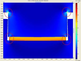
21 Stress distribution

22 Problem Exaggerated deformation plot Room temperature High temperature Bottom end fixed Quartz tube tends to squeeze No room for expansion
 Graphite")

23 Design changes Graphite (6.21 cm Ø curvature) Graphite (6.52 cm Ø curvature) Top graphite radius of curvature reduced


24 Design changes Uniform forces on the sample Both bottom and top graphite radius reduced

25 New Samples SEM of GaAs/GaP bonded interface PIN diodes transferred on GaP substrate Cleaner bonding interfaces Eliminated quartz failure
26 Conclusion & Future Work Basic models developed : to study the electrostatic actuation of spring plates to study behaviour of our PIN diode structure wafer fusion fixture 64 Bit workstation with 28Gb RAM Future work : Study effect of changing spring plate thickness Varying PIN diode dimensions, and photo response

27 Acknowledgement Work partially funded by United States Air Force www. uml.edu/photonics
Modeling PIN Photodiodes
 Modeling PIN Photodiodes Roger W. Pryor*, Ph.D. Pryor Knowledge Systems, Inc. *Corresponding author: 4918 Malibu Drive, Bloomfield Hills, MI 48302, rwpryor@pksez1.com Abstract: This paper presents one
OPTI510R: Photonics. Khanh Kieu College of Optical Sciences, University of Arizona Meinel building R.626
 OPTI510R: Photonics Khanh Kieu College of Optical Sciences, University of Arizona kkieu@optics.arizona.edu Meinel building R.626 Announcements Homework #6 is assigned, due May 1 st Final exam May 8, 10:30-12:30pm
ELECTRONIC DEVICES AND CIRCUITS SUMMARY
 ELECTRONIC DEVICES AND CIRCUITS SUMMARY Classification of Materials: Insulator: An insulator is a material that offers a very low level (or negligible) of conductivity when voltage is applied. Eg: Paper,
OOFELIE::Multiphysics 2014
 OOFELIE::Multiphysics 2014 INDUSTRIAL MULTIPHYSICS DESIGN FOR OPTICAL DEVICES INTRODUCTION 2 High precision opto-mechanics A VERY HIGH ACCURACY IN THE PRODUCTION OF MIRRORS AND LENSES IS NOW VERY OFTEN
Quiz #1 Practice Problem Set
 Name: Student Number: ELEC 3908 Physical Electronics Quiz #1 Practice Problem Set? Minutes January 22, 2016 - No aids except a non-programmable calculator - All questions must be answered - All questions
Integrating MEMS Electro-Static Driven Micro-Probe and Laser Doppler Vibrometer for Non-Contact Vibration Mode SPM System Design
 Tamkang Journal of Science and Engineering, Vol. 12, No. 4, pp. 399 407 (2009) 399 Integrating MEMS Electro-Static Driven Micro-Probe and Laser Doppler Vibrometer for Non-Contact Vibration Mode SPM System
COMSOL Multiphysics Software and Photovoltaics: A Unified Platform for Numerical Simulation of Solar Cells and Modules
 COMSOL Multiphysics Software and Photovoltaics: A Unified Platform for Numerical Simulation of Solar Cells and Modules Marco Nardone, Ph.D. Bowling Green State University Bowling Green, Ohio 1 Photovoltaics
Lecture 2. Semiconductor Physics. Sunday 4/10/2015 Semiconductor Physics 1-1
 Lecture 2 Semiconductor Physics Sunday 4/10/2015 Semiconductor Physics 1-1 Outline Intrinsic bond model: electrons and holes Charge carrier generation and recombination Intrinsic semiconductor Doping:
Determining thermal noise limiting properties of thin films
 Determining thermal noise limiting properties of thin films Courtney Linn Institute for Gravitational Research University of Glasgow Summer 2011 Abstract In order to make thermally stable mirrors to be
Instrumentation and Operation
 Instrumentation and Operation 1 STM Instrumentation COMPONENTS sharp metal tip scanning system and control electronics feedback electronics (keeps tunneling current constant) image processing system data
Thermal Corrective Devices for Advanced Gravitational Wave Interferometers
 Thermal Corrective Devices for Advanced Gravitational Wave Interferometers Marie Kasprzack, Louisiana State University 6 th October 2016 COMSOL Conference 2016 Boston 1 1. Advanced Gravitational Wave Detectors
Lecture 15: Optoelectronic devices: Introduction
 Lecture 15: Optoelectronic devices: Introduction Contents 1 Optical absorption 1 1.1 Absorption coefficient....................... 2 2 Optical recombination 5 3 Recombination and carrier lifetime 6 3.1
ECE 250 Electronic Devices 1. Electronic Device Modeling
 ECE 250 Electronic Devices 1 ECE 250 Electronic Device Modeling ECE 250 Electronic Devices 2 Introduction to Semiconductor Physics You should really take a semiconductor device physics course. We can only
Design and Simulation of A MEMS Based Horseshoe Shaped Low Current Lorentz Deformable Mirror (LCL-DM).
.") Design and Simulation of A MEMS Based Horseshoe Shaped Low Current Lorentz Deformable Mirror (LCL-DM). Byoungyoul Park 1, Tao Chen 1, Cyrus Shafai 1 1 Electrical and Computer Engineering, University of
Design and Simulation of A MEMS Based Horseshoe Shaped Low Current Lorentz Deformable Mirror (LCL-DM). Byoungyoul Park 1, Tao Chen 1, Cyrus Shafai 1 1 Electrical and Computer Engineering, University of
Semiconductor Junctions
 8 Semiconductor Junctions Almost all solar cells contain junctions between different materials of different doping. Since these junctions are crucial to the operation of the solar cell, we will discuss
Blaze/Blaze 3D. Device Simulator for Advanced Materials
 Blaze/Blaze 3D Device Simulator for Advanced Materials Contents Introduction: What is Blaze? Purpose: Why use Blaze? Features Application examples Conclusions - 2 - Introduction Blaze/Blaze 3D simulates
Solution 11:00 AM, Wednesday February 10, 2010, 108 Nedderman Hall 80 minutes allowed (last four digits of your student #) ( if new)
 ( if new)") MidTerm - EE 5342 (print last name) (print first name) Solution 11:00 AM, Wednesday February 10, 2010, 108 Nedderman Hall 80 minutes allowed (last four digits of your student #) (e-mail if new) Instructions:
MidTerm - EE 5342 (print last name) (print first name) Solution 11:00 AM, Wednesday February 10, 2010, 108 Nedderman Hall 80 minutes allowed (last four digits of your student #) (e-mail if new) Instructions:
OPTI510R: Photonics. Khanh Kieu College of Optical Sciences, University of Arizona Meinel building R.626
 OPTI510R: Photonics Khanh Kieu College of Optical Sciences, University of Arizona kkieu@optics.arizona.edu Meinel building R.626 Announcements HW#3 is assigned due Feb. 20 st Mid-term exam Feb 27, 2PM
Introduction to Semiconductor Physics. Prof.P. Ravindran, Department of Physics, Central University of Tamil Nadu, India
 Introduction to Semiconductor Physics 1 Prof.P. Ravindran, Department of Physics, Central University of Tamil Nadu, India http://folk.uio.no/ravi/cmp2013 Review of Semiconductor Physics Semiconductor fundamentals
Semiconductor Physical Electronics
 Semiconductor Physical Electronics Sheng S. Li Department of Electrical Engineering University of Florida Gainesville, Florida Plenum Press New York and London Contents CHAPTER 1. Classification of Solids
Thermo-Mechanical Analysis of a Multi-Layer MEMS Membrane
 Thermo-Mechanical Analysis of a Multi-Layer MEMS Membrane Heiko Fettig, PhD James Wylde, PhD Nortel Networks - Optical Components Ottawa ON K2H 8E9 Canada Abstract This paper examines the modelling of
Y. C. Lee. Micro-Scale Engineering I Microelectromechanical Systems (MEMS)
") Micro-Scale Engineering I Microelectromechanical Systems (MEMS) Y. C. Lee Department of Mechanical Engineering University of Colorado Boulder, CO 80309-0427 leeyc@colorado.edu January 15, 2014 1 Contents
Micro-Scale Engineering I Microelectromechanical Systems (MEMS) Y. C. Lee Department of Mechanical Engineering University of Colorado Boulder, CO 80309-0427 leeyc@colorado.edu January 15, 2014 1 Contents
PHYSICAL SCIENCES PART A
 PHYSICAL SCIENCES PART A 1. The calculation of the probability of excitation of an atom originally in the ground state to an excited state, involves the contour integral iωt τ e dt ( t τ ) + Evaluate the
Design and Development of Bimorph Deformable Mirrors for Defocus Correction
 Design and Development of Bimorph Deformable Mirrors for Defocus Correction Kavita Rawal, Vijayeta Gambhir and D.P Ghai Laser Science and Technology Center, Metcalfe House, Old sectt, Delhi-110054, India.
Single Photon detectors
 Single Photon detectors Outline Motivation for single photon detection Semiconductor; general knowledge and important background Photon detectors: internal and external photoeffect Properties of semiconductor
2.76/2.760 Multiscale Systems Design & Manufacturing
 2.76/2.760 Multiscale Systems Design & Manufacturing Fall 2004 MOEMS Devices for Optical communications system Switches and micromirror for Add/drops Diagrams removed for copyright reasons. MOEMS MEMS
Classification of Solids
 Classification of Solids Classification by conductivity, which is related to the band structure: (Filled bands are shown dark; D(E) = Density of states) Class Electron Density Density of States D(E) Examples
LEC E T C U T R U E R E 17 -Photodetectors
 LECTURE 17 -Photodetectors Topics to be covered Photodetectors PIN photodiode Avalanche Photodiode Photodetectors Principle of the p-n junction Photodiode A generic photodiode. Photodetectors Principle
Introduction to Microeletromechanical Systems (MEMS) Lecture 9 Topics. MEMS Overview
 Lecture 9 Topics. MEMS Overview") Introduction to Microeletromechanical Systems (MEMS) Lecture 9 Topics MicroOptoElectroMechanical Systems (MOEMS) Grating Light Valves Corner Cube Reflector (CCR) MEMS Light Modulator Optical Switch Micromirrors
Introduction to Microeletromechanical Systems (MEMS) Lecture 9 Topics MicroOptoElectroMechanical Systems (MOEMS) Grating Light Valves Corner Cube Reflector (CCR) MEMS Light Modulator Optical Switch Micromirrors
ECE-342 Test 2 Solutions, Nov 4, :00-8:00pm, Closed Book (one page of notes allowed)
") ECE-342 Test 2 Solutions, Nov 4, 2008 6:00-8:00pm, Closed Book (one page of notes allowed) Please use the following physical constants in your calculations: Boltzmann s Constant: Electron Charge: Free
ECE-342 Test 2 Solutions, Nov 4, 2008 6:00-8:00pm, Closed Book (one page of notes allowed) Please use the following physical constants in your calculations: Boltzmann s Constant: Electron Charge: Free
UNIT - IV SEMICONDUCTORS AND MAGNETIC MATERIALS
 1. What is intrinsic If a semiconductor is sufficiently pure, then it is known as intrinsic semiconductor. ex:: pure Ge, pure Si 2. Mention the expression for intrinsic carrier concentration of intrinsic
More Optical Telescopes
 More Optical Telescopes There are some standard reflecting telescope designs used today All have the common feature of light entering a tube and hitting a primary mirror, from which light is reflected
UNIVERSITY OF CALIFORNIA College of Engineering Department of Electrical Engineering and Computer Sciences. EECS 130 Professor Ali Javey Fall 2006
 UNIVERSITY OF CALIFORNIA College of Engineering Department of Electrical Engineering and Computer Sciences EECS 130 Professor Ali Javey Fall 2006 Midterm I Name: Closed book. One sheet of notes is allowed.
ET3034TUx Utilization of band gap energy
 ET3034TUx - 3.3.1 - Utilization of band gap energy In the last two weeks we have discussed the working principle of a solar cell and the external parameters that define the performance of a solar cell.
Open Engineering: Strongly Coupled Multiphysics
 Open Engineering: Strongly Coupled Multiphysics OOFELIE::Multiphysics Sensors And Actuators Multiphysics FSI Multiphyiscs CAE Consulting Vibro Acoustics, Electro- Technics, FSI-CFD, Opto-Thermo Mechanics,
Development of a cryogenic compact interferometric displacement sensor
 Development of a cryogenic compact interferometric displacement sensor Fabián E. Peña Arellano National Astronomical Observatory of Japan Outline of the presentation Motivation: local position sensor for
Photovoltaic cell and module physics and technology
 Photovoltaic cell and module physics and technology Vitezslav Benda, Prof Czech Technical University in Prague benda@fel.cvut.cz www.fel.cvut.cz 6/21/2012 1 Outlines Photovoltaic Effect Photovoltaic cell
TCAD Modeling of Stress Impact on Performance and Reliability
 TCAD Modeling of Stress Impact on Performance and Reliability Xiaopeng Xu TCAD R&D, Synopsys March 16, 2010 SEMATECH Workshop on Stress Management for 3D ICs using Through Silicon Vias 1 Outline Introduction
UNIVERSITY OF CALIFORNIA, BERKELEY College of Engineering Department of Electrical Engineering and Computer Sciences
 UNIVERSITY OF CALIFORNIA, BERKELEY College of Engineering Department of Electrical Engineering and Computer Sciences EECS 40 Spring 2000 Introduction to Microelectronic Devices Prof. King MIDTERM EXAMINATION
Carriers Concentration, Current & Hall Effect in Semiconductors. Prof.P. Ravindran, Department of Physics, Central University of Tamil Nadu, India
 Carriers Concentration, Current & Hall Effect in Semiconductors 1 Prof.P. Ravindran, Department of Physics, Central University of Tamil Nadu, India http://folk.uio.no/ravi/semi2013 Conductivity Charge
EE C247B / ME C218 INTRODUCTION TO MEMS DESIGN SPRING 2014 C. Nguyen PROBLEM SET #4
 Issued: Wednesday, Mar. 5, 2014 PROBLEM SET #4 Due (at 9 a.m.): Tuesday Mar. 18, 2014, in the EE C247B HW box near 125 Cory. 1. Suppose you would like to fabricate the suspended cross beam structure below
Lecture 12. Semiconductor Detectors - Photodetectors
 Lecture 12 Semiconductor Detectors - Photodetectors Principle of the pn junction photodiode Absorption coefficient and photodiode materials Properties of semiconductor detectors The pin photodiodes Avalanche
How Does a Microcantilever Work?
 How Does a Cantilever Work? Participant Guide Description and Estimated Time to Complete The microcantilever is a widely used component in microsystems devices or microelectromechanical systems (MEMS).
Chemistry Instrumental Analysis Lecture 8. Chem 4631
 Chemistry 4631 Instrumental Analysis Lecture 8 UV to IR Components of Optical Basic components of spectroscopic instruments: stable source of radiant energy transparent container to hold sample device
Foundations of MEMS. Chang Liu. McCormick School of Engineering and Applied Science Northwestern University. International Edition Contributions by
 Foundations of MEMS Second Edition Chang Liu McCormick School of Engineering and Applied Science Northwestern University International Edition Contributions by Vaishali B. Mungurwadi B. V. Bhoomaraddi
n N D n p = n i p N A
 Summary of electron and hole concentration in semiconductors Intrinsic semiconductor: E G n kt i = pi = N e 2 0 Donor-doped semiconductor: n N D where N D is the concentration of donor impurity Acceptor-doped
Optimizing micromechanical force detectors for measuring. magnetization at high magnetic fields
 Abstract Optimizing micromechanical force detectors for measuring magnetization at high magnetic fields Jeremy Paster University of Florida July 30, 2008 MEMS devices prove to be advantageous in magnetometry.
XPS/UPS and EFM. Brent Gila. XPS/UPS Ryan Davies EFM Andy Gerger
 XPS/UPS and EFM Brent Gila XPS/UPS Ryan Davies EFM Andy Gerger XPS/ESCA X-ray photoelectron spectroscopy (XPS) also called Electron Spectroscopy for Chemical Analysis (ESCA) is a chemical surface analysis
Slide 1. Temperatures Light (Optoelectronics) Magnetic Fields Strain Pressure Displacement and Rotation Acceleration Electronic Sensors
 Magnetic Fields Strain Pressure Displacement and Rotation Acceleration Electronic Sensors") Slide 1 Electronic Sensors Electronic sensors can be designed to detect a variety of quantitative aspects of a given physical system. Such quantities include: Temperatures Light (Optoelectronics) Magnetic
Slide 1 Electronic Sensors Electronic sensors can be designed to detect a variety of quantitative aspects of a given physical system. Such quantities include: Temperatures Light (Optoelectronics) Magnetic
Plasma Processing in the Microelectronics Industry. Bert Ellingboe Plasma Research Laboratory
 Plasma Processing in the Microelectronics Industry Bert Ellingboe Plasma Research Laboratory Outline What has changed in the last 12 years? What is the relavant plasma physics? Sheath formation Sheath
UNIVERSITY OF CALIFORNIA College of Engineering Department of Electrical Engineering and Computer Sciences. Professor Chenming Hu.
 UNIVERSITY OF CALIFORNIA College of Engineering Department of Electrical Engineering and Computer Sciences EECS 130 Spring 2009 Professor Chenming Hu Midterm I Name: Closed book. One sheet of notes is
December 1999 FINAL TECHNICAL REPORT 1 Mar Mar 98
 REPORT DOCUMENTATION PAGE AFRL-SR- BL_TR " Public reporting burden for this collection of information is estimated to average 1 hour per response, including the time for reviewing instruct the collection
FYS3410 Condensed matter physics
 FYS3410 Condensed matter physics Lecture 23 and 24: pn-junctions and electrooptics Randi Haakenaasen UniK/UiO Forsvarets forskningsinstitutt 11.05.2016 and 18.05.2016 Outline Why pn-junctions are important
CHAPTER 5 FIXED GUIDED BEAM ANALYSIS
 77 CHAPTER 5 FIXED GUIDED BEAM ANALYSIS 5.1 INTRODUCTION Fixed guided clamped and cantilever beams have been designed and analyzed using ANSYS and their performance were calculated. Maximum deflection
KATIHAL FİZİĞİ MNT-510
 KATIHAL FİZİĞİ MNT-510 YARIİLETKENLER Kaynaklar: Katıhal Fiziği, Prof. Dr. Mustafa Dikici, Seçkin Yayıncılık Katıhal Fiziği, Şakir Aydoğan, Nobel Yayıncılık, Physics for Computer Science Students: With
Syllabus: UHH ASTR 450 (F18): Astronomical Instrumentation
: Astronomical Instrumentation") Syllabus: UHH ASTR 450 (F18): Astronomical Instrumentation Prof. Klaus W. Hodapp This course is the final course in the 3-course series on optics and astronomical instrumentation offered at UHH. We will
Syllabus: UHH ASTR 450 (F18): Astronomical Instrumentation Prof. Klaus W. Hodapp This course is the final course in the 3-course series on optics and astronomical instrumentation offered at UHH. We will
Lecture 18. New gas detectors Solid state trackers
 Lecture 18 New gas detectors Solid state trackers Time projection Chamber Full 3-D track reconstruction x-y from wires and segmented cathode of MWPC z from drift time de/dx information (extra) Drift over
Semiconductor Module
 Semiconductor Module Optics Seminar July 18, 2018 Yosuke Mizuyama, Ph.D. COMSOL, Inc. The COMSOL Product Suite Governing Equations Semiconductor Schrödinger Equation Semiconductor Optoelectronics, FD Semiconductor
Modeling PIN Photodiodes. Roger W. Pryor, Ph.D.,VP Research Pryor Knowledge Systems, Inc.
 Presented at the COMSOL Conference 2010 Boston Modeling PIN Photodiodes,VP Research, Inc. PIN Photodiode Modeling This paper presents a new AC/DC Conduction Current Module Model of a PIN Photodiode using
8.1 Drift diffusion model
 8.1 Drift diffusion model Advanced theory 1 Basic Semiconductor Equations The fundamentals of semiconductor physic are well described by tools of quantum mechanic. This point of view gives us a model of
Photonic Communications Engineering Lecture. Dr. Demetris Geddis Department of Engineering Norfolk State University
 Photonic Communications Engineering Lecture Dr. Demetris Geddis Department of Engineering Norfolk State University Light Detectors How does this detector work? Image from visionweb.com Responds to range
Sample Exam # 2 ECEN 3320 Fall 2013 Semiconductor Devices October 28, 2013 Due November 4, 2013
 Sample Exam # 2 ECEN 3320 Fall 203 Semiconductor Devices October 28, 203 Due November 4, 203. Below is the capacitance-voltage curve measured from a Schottky contact made on GaAs at T 300 K. Figure : Capacitance
Technical Report PZT-Silicon Cantilever Benders
 Radiant Technologies, Inc. 2021 Girard SE Albuquerque, NM 876 Tel: 505-842-8007 Fax: 505-842-0366 Technical Report PZT-Silicon Cantilever Benders Subject: Displacement Measurements of Silicon Cantilevers
UNIVERSITY OF CALIFORNIA, BERKELEY College of Engineering Department of Electrical Engineering and Computer Sciences
 UNIVERSITY OF CALIFORNIA, BERKELEY College of Engineering Department of Electrical Engineering and Computer Sciences EE 105: Microelectronic Devices and Circuits Spring 2008 MIDTERM EXAMINATION #1 Time
Section 12: Intro to Devices
 Section 12: Intro to Devices Extensive reading materials on reserve, including Robert F. Pierret, Semiconductor Device Fundamentals Bond Model of Electrons and Holes Si Si Si Si Si Si Si Si Si Silicon
Energetic particles and their detection in situ (particle detectors) Part II. George Gloeckler
 Part II. George Gloeckler") Energetic particles and their detection in situ (particle detectors) Part II George Gloeckler University of Michigan, Ann Arbor, MI University of Maryland, College Park, MD Simple particle detectors Gas-filled
Energetic particles and their detection in situ (particle detectors) Part II George Gloeckler University of Michigan, Ann Arbor, MI University of Maryland, College Park, MD Simple particle detectors Gas-filled
SUPPLEMENTARY NOTES Supplementary Note 1: Fabrication of Scanning Thermal Microscopy Probes
 SUPPLEMENTARY NOTES Supplementary Note 1: Fabrication of Scanning Thermal Microscopy Probes Fabrication of the scanning thermal microscopy (SThM) probes is summarized in Supplementary Fig. 1 and proceeds
Resistance Thermometry based Picowatt-Resolution Heat-Flow Calorimeter
 Resistance Thermometry based Picowatt-Resolution Heat-Flow Calorimeter S. Sadat 1, E. Meyhofer 1 and P. Reddy 1, 1 Department of Mechanical Engineering, University of Michigan, Ann Arbor, 48109 Department
DESIGN, FABRICATION AND ELECTROMECHANICAL CHARACTERISTICS OF A MEMS BASED MICROMIRROR
 XIX IMEKO World Congress Fundamental and Applied Metrology September 6 11, 2009, Lisbon, Portugal DESIGN, FABRICATION AND ELECTROMECHANICAL CHARACTERISTICS OF A MEMS BASED MICROMIRROR Talari Rambabu 1,
Introduction to semiconductor nanostructures. Peter Kratzer Modern Concepts in Theoretical Physics: Part II Lecture Notes
 Introduction to semiconductor nanostructures Peter Kratzer Modern Concepts in Theoretical Physics: Part II Lecture Notes What is a semiconductor? The Fermi level (chemical potential of the electrons) falls
junctions produce nonlinear current voltage characteristics which can be exploited
 Chapter 6 P-N DODES Junctions between n-and p-type semiconductors are extremely important foravariety of devices. Diodes based on p-n junctions produce nonlinear current voltage characteristics which can
MICRO-SCALE SHEET RESISTANCE MEASUREMENTS ON ULTRA SHALLOW JUNCTIONS
 MICRO-SCALE SHEET RESISTANCE MEASUREMENTS ON ULTRA SHALLOW JUNCTIONS Christian L. Petersen, Rong Lin, Dirch H. Petersen, Peter F. Nielsen CAPRES A/S, Burnaby, BC, Canada CAPRES A/S, Lyngby, Denmark We
Mat. Res. Soc. Symp. Proc. Vol Materials Research Society
 Mat. Res. Soc. Symp. Proc. Vol. 738 2003 Materials Research Society G7.26.1 Determination of the Plastic Behavior of Low Thermal Expansion Glass at the Nanometer Scale Richard Tejeda, 1 Roxann Engelstad,
Ion Concentration and Electromechanical Actuation Simulations of Ionic Polymer-Metal Composites
 October 5-7, 2016, Boston, Massachusetts, USA Ion Concentration and Electromechanical Actuation Simulations of Ionic Polymer-Metal Composites Tyler Stalbaum, Qi Shen, and Kwang J. Kim Active Materials
Simulation of a Polyimide Based Micromirror
 Simulation of a Polyimide Based Micromirror A. Arevalo* *1, S. Ilyas **1, D. Conchouso and I. G. Foulds *1, 2 * Computer, Electrical and Mathematical Sciences and Engineering Division (CEMSE), ** Physical
3.15 Electrical, Optical, and Magnetic Materials and Devices Caroline A. Ross Fall Term, 2005
 3.15 Electrical, Optical, and Magnetic Materials and Devices Caroline A. Ross Fall Term, 2005 Exam 2 (5 pages) Closed book exam. Formulae and data are on the last 3.5 pages of the exam. This takes 80 min
Session 6: Solid State Physics. Diode
 Session 6: Solid State Physics Diode 1 Outline A B C D E F G H I J 2 Definitions / Assumptions Homojunction: the junction is between two regions of the same material Heterojunction: the junction is between
3. Two-dimensional systems
 3. Two-dimensional systems Image from IBM-Almaden 1 Introduction Type I: natural layered structures, e.g., graphite (with C nanostructures) Type II: artificial structures, heterojunctions Great technological
Semiconductor Physics fall 2012 problems
 Semiconductor Physics fall 2012 problems 1. An n-type sample of silicon has a uniform density N D = 10 16 atoms cm -3 of arsenic, and a p-type silicon sample has N A = 10 15 atoms cm -3 of boron. For each
Institute for Electron Microscopy and Nanoanalysis Graz Centre for Electron Microscopy
 Institute for Electron Microscopy and Nanoanalysis Graz Centre for Electron Microscopy Micromechanics Ass.Prof. Priv.-Doz. DI Dr. Harald Plank a,b a Institute of Electron Microscopy and Nanoanalysis, Graz
16EC401 BASIC ELECTRONIC DEVICES UNIT I PN JUNCTION DIODE. Energy Band Diagram of Conductor, Insulator and Semiconductor:
 16EC401 BASIC ELECTRONIC DEVICES UNIT I PN JUNCTION DIODE Energy bands in Intrinsic and Extrinsic silicon: Energy Band Diagram of Conductor, Insulator and Semiconductor: 1 2 Carrier transport: Any motion
Modelling of Different MEMS Pressure Sensors using COMSOL Multiphysics
 International Journal of Current Engineering and Technology E-ISSN 2277 4106, P-ISSN 2347 5161 2017 INPRESSCO, All Rights Reserved Available at http://inpressco.com/category/ijcet Research Article Modelling
Department of Electrical and Computer Engineering, Cornell University. ECE 3150: Microelectronics. Spring Exam 1 ` March 22, 2018
 Department of Electrical and Computer Engineering, Cornell University ECE 3150: Microelectronics Spring 2018 Exam 1 ` March 22, 2018 INSTRUCTIONS: Every problem must be done in the separate booklet Only
Figure 3.1 (p. 141) Figure 3.2 (p. 142)
 Figure 3.2 (p. 142)") Figure 3.1 (p. 141) Allowed electronic-energy-state systems for two isolated materials. States marked with an X are filled; those unmarked are empty. System 1 is a qualitative representation of a metal;
Figure 3.1 (p. 141) Allowed electronic-energy-state systems for two isolated materials. States marked with an X are filled; those unmarked are empty. System 1 is a qualitative representation of a metal;
Structural Optimization of Silicon Carbide PIN Avalanche Photodiodes for UV Detection
 Journal of the Korean Physical Society, Vol. 56, No. 2, February 2010, pp. 672 676 Structural Optimization of Silicon Carbide PIN Avalanche Photodiodes for UV Detection Ho-Young Cha School of Electronic
Piezoelectric Resonators ME 2082
 Piezoelectric Resonators ME 2082 Introduction K T : relative dielectric constant of the material ε o : relative permittivity of free space (8.854*10-12 F/m) h: distance between electrodes (m - material
CHAPTER 4 DESIGN AND ANALYSIS OF CANTILEVER BEAM ELECTROSTATIC ACTUATORS
 61 CHAPTER 4 DESIGN AND ANALYSIS OF CANTILEVER BEAM ELECTROSTATIC ACTUATORS 4.1 INTRODUCTION The analysis of cantilever beams of small dimensions taking into the effect of fringing fields is studied and
Solid State Electronics. Final Examination
 The University of Toledo EECS:4400/5400/7400 Solid State Electronic Section elssf08fs.fm - 1 Solid State Electronics Final Examination Problems Points 1. 1. 14 3. 14 Total 40 Was the exam fair? yes no
e - Galvanic Cell 1. Voltage Sources 1.1 Polymer Electrolyte Membrane (PEM) Fuel Cell
 Fuel Cell") Galvanic cells convert different forms of energy (chemical fuel, sunlight, mechanical pressure, etc.) into electrical energy and heat. In this lecture, we are interested in some examples of galvanic cells.
Galvanic cells convert different forms of energy (chemical fuel, sunlight, mechanical pressure, etc.) into electrical energy and heat. In this lecture, we are interested in some examples of galvanic cells.
Non-Linear Finite Element Modeling of THUNDER Piezoelectric Actuators
 Non-Linear Finite Element Modeling of THUNDER Piezoelectric Actuators Barmac K. Taleghani 1, Joel F. Campbell 2 1 Army Research Laboratory, Vehicle Technology Center, MS 230 NASA Langley Research Center,
6.012 Electronic Devices and Circuits
 Page 1 of 1 YOUR NAME Department of Electrical Engineering and Computer Science Massachusetts Institute of Technology 6.12 Electronic Devices and Circuits Exam No. 1 Wednesday, October 7, 29 7:3 to 9:3
Design And Analysis of Microcantilevers With Various Shapes Using COMSOL Multiphysics Software
 Design And Analysis of Microcantilevers With Various Shapes Using COMSOL Multiphysics Software V. Mounika Reddy 1, G.V.Sunil Kumar 2 1,2 Department of Electronics and Instrumentation Engineering, Sree
Current mechanisms Exam January 27, 2012
 Current mechanisms Exam January 27, 2012 There are four mechanisms that typically cause currents to flow: thermionic emission, diffusion, drift, and tunneling. Explain briefly which kind of current mechanisms
pn JUNCTION THE SHOCKLEY MODEL
 The pn Junction: The Shockley Model ( S. O. Kasap, 1990-001) 1 pn JUNCTION THE SHOCKLEY MODEL Safa Kasap Department of Electrical Engineering University of Saskatchewan Canada Although the hole and its
LASER INTERFEROMETER GRAVITATIONAL WAVE OBSERVATORY - LIGO - CALIFORNIA INSTITUTE OF TECHNOLOGY MASSACHUSETTS INSTITUTE OF TECHNOLOGY
 LASER INTERFEROMETER GRAVITATIONAL WAVE OBSERVATORY - LIGO - CALIFORNIA INSTITUTE OF TECHNOLOGY MASSACHUSETTS INSTITUTE OF TECHNOLOGY Document Type LIGO-T960148-01- D Sep / 9 / 96 Maximum Current of the
Junction Diodes. Tim Sumner, Imperial College, Rm: 1009, x /18/2006
 Junction Diodes Most elementary solid state junction electronic devices. They conduct in one direction (almost correct). Useful when one converts from AC to DC (rectifier). But today diodes have a wide
Semiconductor X-Ray Detectors. Tobias Eggert Ketek GmbH
 Semiconductor X-Ray Detectors Tobias Eggert Ketek GmbH Semiconductor X-Ray Detectors Part A Principles of Semiconductor Detectors 1. Basic Principles 2. Typical Applications 3. Planar Technology 4. Read-out
Novel High-Efficiency Crystalline-Si-Based Compound. Heterojunction Solar Cells: HCT (Heterojunction with Compound. Thin-layer)
") Electronic Supplementary Material (ESI) for Physical Chemistry Chemical Physics. This journal is the Owner Societies 2014 Supplementary Information for Novel High-Efficiency Crystalline-Si-Based Compound
Electronic Supplementary Material (ESI) for Physical Chemistry Chemical Physics. This journal is the Owner Societies 2014 Supplementary Information for Novel High-Efficiency Crystalline-Si-Based Compound
CBSE PHYSICS QUESTION PAPER (2005)
") CBSE PHYSICS QUESTION PAPER (2005) (i) (ii) All questions are compulsory. There are 30 questions in total. Questions 1 to 8 carry one mark each, Questions 9 to 18 carry two marks each, Question 19 to 27
CBSE PHYSICS QUESTION PAPER (2005) (i) (ii) All questions are compulsory. There are 30 questions in total. Questions 1 to 8 carry one mark each, Questions 9 to 18 carry two marks each, Question 19 to 27
Semiconductor-Detectors
 Semiconductor-Detectors 1 Motivation ~ 195: Discovery that pn-- junctions can be used to detect particles. Semiconductor detectors used for energy measurements ( Germanium) Since ~ 3 years: Semiconductor